CDF Run II Silicon Vertex Detector Annealing Study
Abstract
Between Run II commissioning in early 2001 and the end of operations in September 2011, the Tevatron collider delivered 12 fb-1 of collisions at TeV to the Collider Detector at Fermilab (CDF). During that time, the CDF silicon vertex detector was subject to radiation doses of up to 12 Mrad. After the end of operations, the silicon detector was annealed for 24 days at 18. In this paper, we present a measurement of the change in the bias currents for a subset of sensors during the annealing period. We also introduce a novel method for monitoring the depletion voltage throughout the annealing period. The observed bias current evolution can be characterized by a falling exponential term with time constant (stat.)(syst.) days. We observe an average decrease of in the depletion voltage, whose evolution can similarly be described by an exponential time constant of days. These results are consistent with the Hamburg model within the measurement uncertainties.
keywords:
Annealing , Silicon , Vertex Detector , CDF , Detector Operations1 Introduction
In high-energy physics (HEP) experiments, silicon sensors serve a crucial role in the detection of charged particle positions, momenta, and to some extent, information. Due to their typically close location to the collision point of hadron colliders, silicon sensors often incur intense radiation damage due to the numerous particles from collisions that traverse them. The macroscopic effects of radiation damage on silicon sensors in HEP detectors has been extensively studied. The leakage currents increase linearly with radiation dose, and for -bulk sensors, the depletion voltage initially decreases until the sensor appears to undergo type inversion, at which point then increases with radiation dose. These macroscopic changes have been linked to the formation of crystal defects when atoms are displaced from their lattice positions after collisions with particles from the radiation field.
The process of annealing is the opposite effect, where increasing the temperature of the silicon sensor allows the displaced atoms to settle back into vacant lattice positions, eliminating the local crystal defect, and at least partially recovering some of the initial behavior of the silicon sensor as it was before irradiation. Annealing, which is strongly temperature dependent, has been studied with test sensors, where the irradiation phase and the annealing phase can be isolated from each other by strict temperature controls. Such temperature control enables the construction of silicon-behavior models which can closely approximate ideal silicon sensor behavior. The most popular of them is the Hamburg model [1, 2] whose verification and that other models is ongoing.
Because annealing can prolong the life of a HEP silicon detector, understanding how the macroscopic quantities such as leakage current and depletion voltage change with time for different temperatures is of great interest to the HEP silicon detector community. Test bench studies are usually done at warm (40-80) temperatures to maximize the annealing effect in the available time, while annealing of HEP detectors is more practical at room temperature.
This article describes the annealing studies that were performed with the silicon detector system at the CDF experiment at Fermi National Accelerator Laboratory. The silicon sensors were exposed to 0.4-12 of radiation over the course of 10 years, and dedicated annealing studies were performed after the end of Tevatron Run II. This in-situ measurement of annealing with an operating HEP detector required a new method for monitoring the depletion voltage of the sensors. We discuss some annealing theory in Sec. 2 and the detector in Sec. 3. The measurement and monitoring procedures are detailed in Sec. 4. The analysis of the current changes and depletion voltages are given in Secs. 5 and 6 and the results and conclusions follow in the remaining sections.
2 Silicon Annealing
The behavior of a silicon detector can be characterized by several quantities. For this study, we consider the leakage current, and the depletion voltage , which for an unirradiated sensor is defined as the minimum bias voltage applied to the sensor that can deplete it of free charge carriers. As the silicon sensors are irradiated, the behavior of these quantities changes. The leakage current increases in a manner linearly proportional to the fluence:
| (1) |
where is the current related damage rate, is the fluence, and is the volume of the sensor. is the increase in leakage current from its original value . The magnitude of is temperature-dependent and on the order of A/cm.
| Term | 1 | 2 | 3 | 4 | 5 | 6 |
|---|---|---|---|---|---|---|
| at 18 (days) | ||||||
| at 11 (days) | ||||||
| at -5 (days) | ||||||
During annealing, the leakage current is observed to decrease and the rate of this decrease strongly depends on temperature, based on studies performed in the temperature range 0-60. The decrease of the leakage current is often parameterized according to the Hamburg model, which suggests a leakage-current evolution according to the formula:
| (2) |
In this expression, represents the start time of annealing and the sum is over different types of crystal defects, each of which has a temperature-dependent characteristic time constant and an amplitude , subject to the constraint . Table 1 shows characteristic values for the constants and for the annealing temperature of 18, and also 11 and -5, which are the the nominal operating temperatures of the SVX and L00 CDF silicon subdetectors, respectively (see Sec. 3). Note that the weights are not temperature dependent, but the time constants scale according to the Arrhenius equation.
Figure 1 shows the expected leakage current behavior during annealing for annealing temperatures of 15, 18 and 21 . As can be seen, the leakage current is at its maximum immediately after warming, and then decreases due to the annealing behavior as described in Eq. (2).
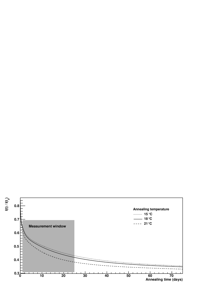
The shaded region in Fig. 1 corresponds to the period when CDF annealing data were recorded. As the time constants of the individual terms in Eq. (2) span several orders of magnitude, the measurements presented are sensitive to only a subset of the parameters in Eq. (2). A more appropriate parameterization is thus
| (3) |
where and are empirical constants, and is a time constant associated with annealing; it is calculated to be 17.6 days, as discussed in Sec. 8.1.
The change in the depletion voltage during annealing occurs in a more complicated fashion. According to the Hamburg model, as the sensor is irradiated with an accumulated fluence , changes proportionally to any adjustments in the effective doping concentration:
| (4) |
where is the annealing time, and , and represent contributions from short-term annealing, a stable damage component independent of annealing time, and reverse-annealing, respectively. As we are primarily interested in the time-dependence of annealing, merely serves as an overall offset, and so we do not specify its explicit form. The short-term and reverse annealing components, are given by:
| (5) | ||||
| (8) |
where the dependencies on the fluence have been absorbed by the constants and . An explanation of the definitions and differences of first- and second-order processes can be found in Ref. [1].
At room temperature, reverse-annealing has a time scale on the order of 500 days [1], for which both first- and second-order processes can be approximated for this analysis by a term linear in annealing time: , where is the 500-day time constant. We therefore expect the depletion voltage to follow
| (9) |
where and represent offsets, and is the constant associated with reverse-annealing. The short-term annealing time constant is expected to be days, based on parameters given in Ref. [1], and scaling to 18 using the Arrhenius equation. Note that the value of this time constant is expected to be much less than that of Eq. (3).
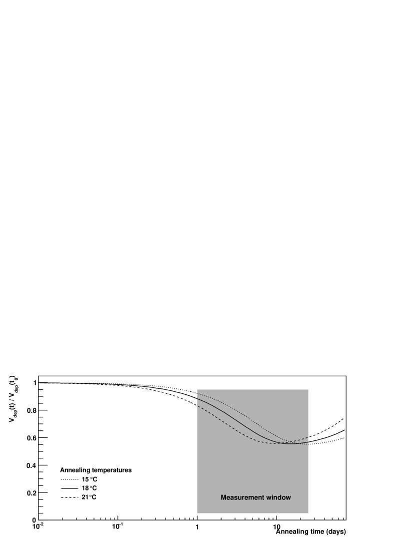
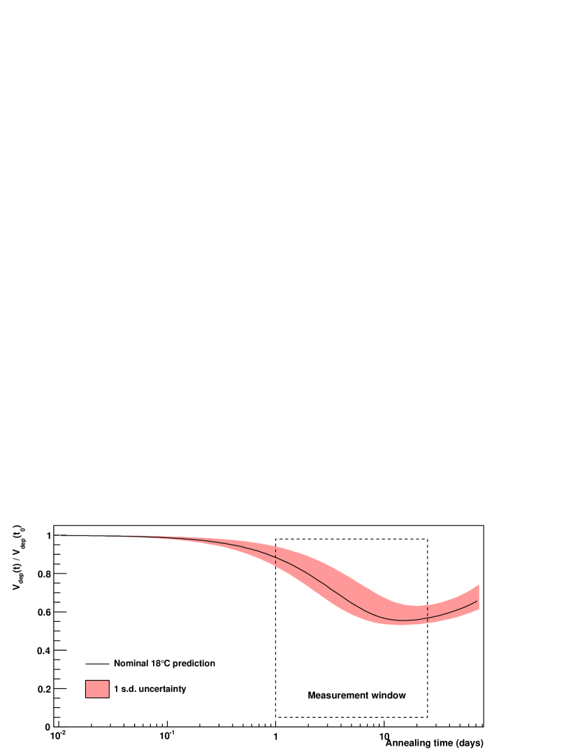
To illustrate the temperature dependence on the predicted annealing behavior of , we plot the Hamburg-model prediction assuming annealing temperatures of 15, 18, and 21 , shown in the top plot of Fig. 2. For these predictions, we use values of , and based on estimates made specifically for the L00 narrow ladders of the CDF silicon detector (see Sec. 3). The lower plot of Fig. 2 shows the nominal prediction for the annealing behavior at 18, and also shows the uncertainty in that prediction, based on estimates in the model parameters as derived in Ref. [1]. Note that whereas is expected to reach a minimum at some point during annealing, the same behavior is not expected for the leakage current, which decreases monotonically as a function of annealing time.
Assuming the Hamburg model appropriately describes the behavior of the silicon sensors at CDF, we expect the after-before depletion voltage ratio to reach a minimum before the end of the measurement window, reaching a value somewhere between 50% and 65% assuming no annealing prior to the end of Run II. Due to scheduling constraints, we were unfortunately unable to extend the measurement window to distinguish between an asymptote and a minimum.
3 The CDF Silicon Detector
The CDF silicon detector system [10] consisted of three sub-detectors, all with barrel geometry: Layer 00 (L00), the Silicon Vertex detector (SVX) and the Intermediate Silicon Layers (ISL). Unless otherwise stated, “detector” refers to the CDF silicon detector. Figure 3 presents the schematic layout of the CDF silicon detector. The design had eight silicon layers to provide tracking which was robust against failure or degradation of individual components.
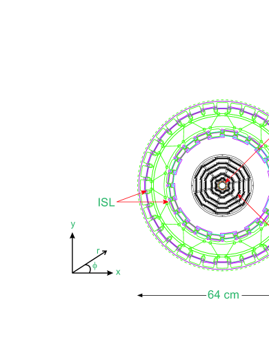
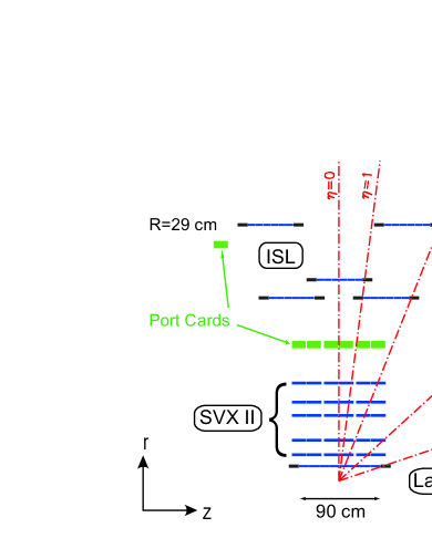
The basic structural unit of a sub-detector was a ladder, which consisted of several silicon microstrip sensors bonded in series (3 sensors for L00 ladders, 4 in SVX ladders and 6 in ISL ladders). Only L00 sensors and SVX sensors in layers 0, 1 and 3 were used in this study. SVX sensors in layers 2 and 4 developed complicated noise profiles making simple data analysis described in this paper unfeasible. The ISL ladders were located too far from the beamline to receive significant dose of radiation and were therefore not of interest for this study, and are not discussed further in this paper.
The sensors were made from high-resistivity -type silicon with a nominal thickness of 300 . Sensors in L00 were single-sided, providing - information, while sensors in the other layers were double-sided, providing both - and - information.
A full ladder was read out from both ends through SVX3D readout chips mounted on electrical hybrids, located outside (for L00) or inside (for SVX) of the tracking volume. Multiple readout chips were chained together to read out a single silicon sensor. A circuit board called the portcard was located at the periphery of each support structure or bulkhead and formed an interface with the hybrids and readout chips with the rest of the data acquisition system.
Layer 00 was a single-sided, single-layer silicon microstrip detector whose sensors were grouped into 48 ladders. It was mounted on a carbon fiber support structure which in turn was mounted directly on the beam pipe. The L00 ladders are classified as narrow or wide, based on the azimuthal extent of the ladder. Narrow ladders were positioned closest to the beam pipe at a radius of 1.35 cm; the wide ladders were located farther away from the beam pipe at a radius of 1.62 cm.
The SVX detector was built in three cylindrical barrels each 29 cm long. Each barrel contained five layers of double-sided silicon microstrips placed along the beam axis, with radial coverage from 2.5 to 10.7 cm. Carbon fiber reinforced Rohacell foam [7] provided support to the ladders, and beryllium bulkheads provided additional support and alignment on each end. Therefore the detector consisted of six bulkheads (-segmentation), each divided into 12 wedges (-segmentation) consisting of 5 layers (-segmentation).
The CDF silicon detector used power supply modules manufactured by CAEN, model number A509 for SVX and model number A509H for L00. These custom modules were housed in SY527 mainframe crates located in the corners of the CDF collision hall. One power supply module provided low voltages (2 V and 5 V) to the portcard, low voltages (5–8 V) to the SVX3D chip chains, and high voltage (up to 500 V) to bias the sensors of one wedge of the silicon detector. L00 ladders had two bias voltage lines. One voltage line was connected to one of the three L00 ladder sensors while the second one was used for the other two.
The SVX and L00 sensors shared a common cooling system to remove the heat generated by the readout chips and maintain a constant operating temperature for the silicon sensors. The temperature of the coolant exiting the chiller was . The SVX sensors were not in close thermal contact with the coolant and their temperatures were not directly monitored. However, by combining the measurements of the ambient and coolant temperatures as a function of time with a finite element thermal model and a dedicated post-run measurement, the temperatures of the sensors during data-taking conditions are estimated to be between 10 and 12 for SVX. For the L00 sensors, cooling was achieved through thermal contact to aluminum tubes glued to the mechanical supports. The L00 readout chips were distant from the sensors, and cooled by separate cooling lines, allowing a temperature of -2.5 for the L00 sensors during data taking operations.
The radiation dose the detector was exposed to was estimated using TLD measurements of the radiation field in the CDF tracking volume [8], extrapolated to the location of the individual silicon layers. The equivalent dose from 1 MeV neutrons can be approximated by assuming that the contributions from photons and low-energy neutrons to the TLD measurements are negligible and that the damage is caused primarily by high-energy charged pions. This results in the relations 1 Mrad high-energy pions/ 1 MeV neutron/ equivalent.
Table 2 provides information about the number of ladders in each layer used in this measurement, distance from the beamline, estimated radiation dose, as well as operating voltage and bias current at the end of Run II. The bias currents in sensors from the same layer vary by %, largely due to temperature differences among the sensors. It is worth noting that only one sensor per L00 ladder was used in this measurement because the bias voltage lines connected to two sensors drew too much current to be powered at 18.
| L00N | L00W | SVX-L0 | SVX-L1 | SVX-L3 | |
| Number of ladders | 12 | 36 | 72 | 72 | 72 |
| Sensors per ladder | 3 | 3 | 2 | 2 | 2 |
| Distance from detector axis | 1.35 cm | 1.62 cm | 2.54 cm | 4.12 cm | 8.22 cm |
| Expected dose | 11.5 Mrad | 8.7 Mrad | 4.5 Mrad | 2.2 Mrad | 0.76 Mrad |
| Average per sensor | 200 A | 250 A | 500 A | 400 A | 300 A |
| Power supply limit per line | 3000 A | 6000 A | 5000 A | 5000 A | 5000 A |
| Sensor temperature | -3 | -3 | 11 | 11 | 11 |
| Max. operating voltage | 500 V | 500 V | 200 V | 200 V | 200 V |
| Final operating voltage | 365 V | 300 V | 170 V | 100-130 V | 100 V |
4 Measurement Procedure
The annealing measurement presented in this paper lasted for 24 days. The results are based on the measurements of curves of the sensors and the evolution of these curves as a function of annealing time. For this study, the detector was warmed up from operating temperature described in the previous section to 18. Higher temperatures were desired for the annealing measurement, but could not be reached due to current in the bias lines exceeding the power supply limit. Because the bias current is very sensitive to the temperature of the ladder, attempts have been made to minimize the effects of ladder self-heating and cross-heating from other ladders used in the study. Unless otherwise stated, detector/ladder OFF state in this paper refers to both high and low voltages set to 0 volts and detector/ladder ON state refers to both high and low voltages set to their nominal values.
4.1 Power Supply Modifications
As stated earlier, CAEN power supply modules provided low voltages to the portcard, low voltages to the SVX3D chip chains, and high voltage to bias the sensors of one wedge of the silicon detector. A safety feature prevented the modules from powering ON the high voltage (HV) channels without first ensuring that the corresponding low voltage (LV) channels are ON. Another safety feature of the power supply modules prevented them to be powered ON when one or more HV or LV cables are disconnected. In other words, in the Run II operating configuration, it was impossible to apply bias voltage without switching on power to the portcards and readout chip chains. When powered, these electronics provided significant heat to the sensors. Therefore, modifications were needed to the power module configuration in order to decouple the HV and LV channels and apply bias voltage with LV cables disconnected.
4.2 scan software
Custom software was developed in order to perform automatic scans. A scan consisted of varying the bias voltage from 0 to in multiple steps for a particular ladder. The value of depended on the detector layer to which the ladder belonged. The step size was also layer dependent and typically in the range of 5–10 V. Not more than two L00 ladders were scanned simultaneously to avoid the effects of cross-heating. Moreover, any ladders scanned in parallel were required to be well separated in the detector volume. For such configurations, the effects of cross-heating were proved to be negligible by observing no change in the bias current for one of the ladders while the other was powered on and off.
4.3 Detector Monitoring
Monitoring software was developed to ensure successful execution of the annealing study. The , -vs.-time and -vs.-time curves were stored for each scan and checked each day. Any changes in operating temperature outside the allowed tolerance triggered an alarm.
4.4 Timeline of the Measurement
Preparation for the measurements started on 09/30/2011, the official end of the Tevatron Run II. Dedicated scans with L00 and SVX low voltage ON were performed. These data help determine the overall change in depletion voltage during the annealing period. L00 and SVX were switched OFF after these scans, and the chiller set point temperature raised to -5 to avoid freezing in the ISL cooling pipes.
On 10/3/2011, the modifications to the power supply modules were completed, and the LV cables were left disconnected from the power supplies until the final day of the study. In parallel, the interlock system settings were changed to allow powering up the detector at temperatures higher than allowed during data taking. The warm-up started on 10/4/2011 and was performed by raising the chiller set point temperature in three steps: to 5, to 15, and to 18. The warm-up stages were separated by three hours in time to allow the temperature in the detector volume to stabilize. scans were performed at the end of each stage of the warm-up.
From 10/4/2011 to 10/27/2011, stable thermal conditions were maintained, except for two malfunctions of the chiller that regulated the coolant temperature. These resulted in colder temperatures for 2-3 hours, and data acquired during these periods were discarded. scans were performed on groups of 2 L00 ladders at a time, with each ladder being scanned roughly every 21 hours. The temperature of the detector volume and the status of the power supply modules were closely monitored.
On 10/28/2011, the chiller set point was lowered from from 18 to 9 to measure bias currents of the SVX ladders at a controlled temperature, uniform across the ladders. These data were used to determine the operating temperature of the SVX ladders reported in Table 2. On 10/30/2011, the chiller set point was lowered to 0 to provide stable and uniform thermal conditions for the L00 ladders. The bias current of each L00 ladder was measured both at the full operating voltage and half the operating voltage. Only one ladder was powered at a time for maximum thermal stability. These data were used to determine the thermal coupling constants for each ladder, needed for the self-heating corrections discussed in A.
Finally, on 10/31/2011, the LV cables were reconnected to the power supply modules, the chiller set point lowered to -10, and the LV power turned on. Another set of scans under operating (data taking) conditions was recorded. The change in depletion voltage over the annealing period was determined by comparing these scans with those taken before the warm up with the same thermal conditions.
5 Bias Current Evolution
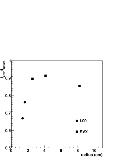
The change in bias current during the annealing period in two ways. We first measure the fractional change over the entire annealing period by comparing the bias current measured under operational thermal conditions before and after the annealing period. Under these thermal conditions, the self heating of the ladders is negligible. Figure 4 shows , the ratio of the bias current after the annealing to that before the annealing, as a function of radial distance from the beam axis. The average is taken over all functional ladders in the layer.
Secondly, we track the bias current evolution over the course of annealing. By examining the current measured at the largest voltage of each IV scan, roughly every 21 hours, the shape of the bias current decrease can be examined. The self-heating of the sensors is substantial under these circumstances, increasing the temperature as much as 3. The bias currents have a strong temperature dependence, increasing roughly 10% for every degree increase in temperature [9]. Thus, the measured currents must be corrected back to the equivalent current at 18.2 before information about the annealing processes can be extracted. It is assumed that the temperature increase is linearly proportional to the power dissipated by the ladder, and the constant of proportionality , unique to each ladder, was determined with a dedicated measurement described in A. Only the narrow ladders of L00 are used for the warm-temperature measurements. This is because the wide ladders dissipate 3-4 times more heat due to their larger sensor volume, and they have a weaker coupling to the cooling system, which introduces complications to the self-heating correction procedure.
Figure 5 shows the data for a typical L00 narrow ladder. The measured currents at the full voltage are shown as a function of annealing time with red squares. The blue circles represent the equivalent current at 18.2. The annealing time dependence of the corrected currents is fit to Eq. (3), and the fit result is shown as a solid line.
An alternate fit function, with an additional exponential term, was considered. However, the uncertainties on the parameters of the additional term were large, suggesting that it is not needed to describe the data. This is discussed further in Sec. 7.
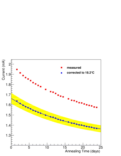
The uncertainty on the parameter in the temperature correction determines the shaded uncertainty band shown around the best fit in Fig. 5, and is used to determine the systematic uncertainty on the time constant of the decaying exponential. A compilation of the fit results for all ladders is presented in Sec. 7.
6 Depletion Voltage Changes
As mentioned in Sec. 2, the behavior of a silicon sensor is partially characterized by the depletion voltage , which is the minimum bias voltage that depletes the active detector region of any charge carriers. In the context of test beam setups, the value of is determined by measuring the capacitance of the sensor as a function of . The curve exhibits a kink at high voltage, and the intersection of two lines that describe the data before and after the kink unambiguously defines . For an operating experiment, the capacitance cannot be measured directly (as in a test setup for a bare sensor), so an alternate definition of is used, which corresponds to the voltage that maximizes the signal collection in a given data-collection time window (see Ref. [10] for details).
For the annealing study presented here, a signal source (i.e. source of charged particles) was not available, thus requiring an alternate method to determine . As the shape of the curve is the only feature from which we can infer the internal properties of the silicon sensor, we develop a metric called , which is a quantity extracted from a fit to the characteristic itself, as discussed in Sec. 6.1.
We use to measure two quantities:
6.1 Fit Procedure
For each scan taken, the data are fit to a function, motivated by the Shockley formula for a - junction [9], and an additional term linear in , which accounts for radiation-damage effects, approximated by a resistor placed in parallel with a - junction:
| (10) |
where the represent parameters to be fitted. The data are fit using 80% of the voltage range, so as to minimize potential residual self-heating effects that can occur at the largest voltages. The uncertainties assumed correspond to half of the spread of the measured bias current for a given voltage setting, after effects from self-heating have stabilized. Typically this uncertainty is on the order of a few . An additional uncertainty of 1 , corresponding to the uncertainty of the least-significant bit, is added in quadrature to this spread.
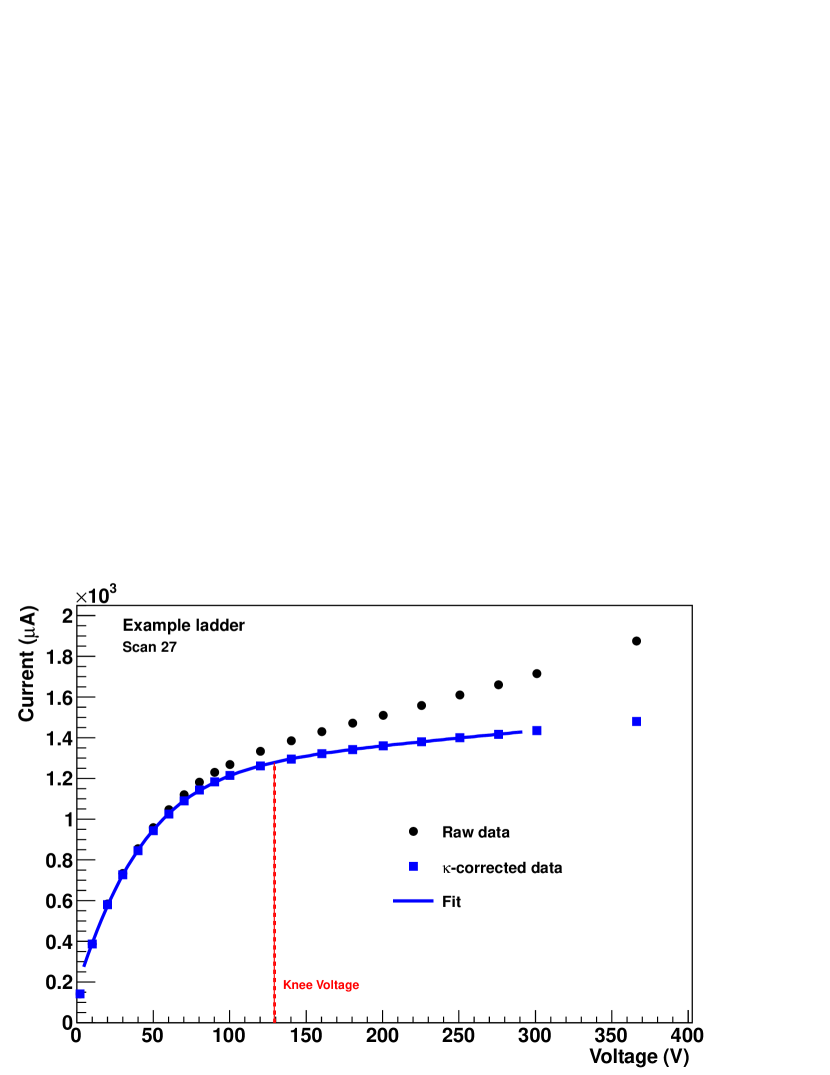
We define the knee voltage as the voltage where the slope of the fit reaches 5% of its maximum value, relative to the difference of the maximum and minimum slopes. The uncertainty in is determined by propagating the uncertainties on the fit parameters (assumed to be Gaussian-distributed about their central values), using a pseudo experiment study that accounts for the fit-parameter correlations.
Figure 6 shows an example fit for one of the L00 ladders. The original, uncorrected data points are shown as black circles, and the -corrected points as blue squares. The fit is performed on the -corrected points, using the parameterization of Eq. (10). Also shown is the extracted knee voltage, and its associated uncertainty (which is on the order of a few V, and thus difficult to see for this particular fit). As illustrated in Fig. 6, the effect of the self-heating correction (A) can be significant at higher voltages. This behavior is not observed for low-voltage ON scans, which were performed at low temperatures. The corrections are thus omitted for the analysis of the LV ON scans, which are described in Sec. 6.2.
6.2 Overall Relative Change in
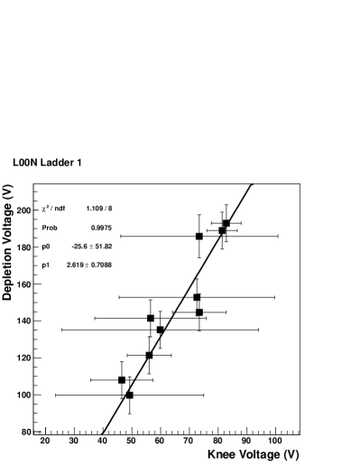
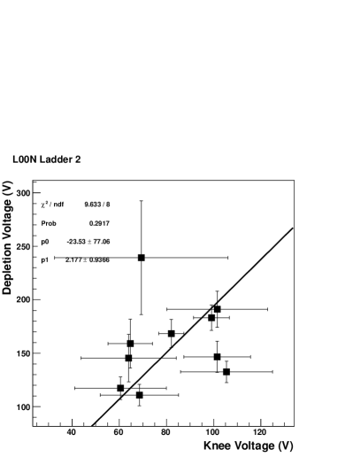
As mentioned in Sec. 4.4, separate low-voltage (LV) ON scans, corresponding to operating conditions, were taken before and after the annealing period. Although we have no signal source to infer values for these scans, we develop a map between and for the L00 ladders. To construct such a map, we use information from the scans performed during nominal CDF running that determined the actual depletion voltage , and the corresponding value derived from fits to the data using the same functional form as shown in Eq. (10). We take the extracted values and plot them against the measured values, and then use an analytical expression to relate the two sets of values.
Whereas the determination of each nominal-running scan is usually reliable, the value often includes large uncertainties. This is a result of increased radiation damage on the silicon ladder as a function of integrated luminosity. We therefore assume a simple linear parameterization , which associates a given value of to . Some sample mappings are given in Fig. 7.
Using these linear mappings, we take the measured values from the LV ON scans before and after annealing and associate them with mapped depletion voltages . We then infer the decrease in mapped depletion voltage, by forming the ratio , where corresponds to the mapped depletion voltage before annealing. This quantity is measured for eleven L00 ladders, and the result from each ladder is combined into a global average, presented in Sec. 7.
Note that by using these mappings, we assume that:
-
1.
serves as a reliable metric of the curves that associates the data to a unique value of the depletion voltage , and
-
2.
as a mapping can be made only of pre-annealed data, we assume that the behavior of before annealing corresponds to its behavior afterward.
6.3 Evolution
Although it would have been desirable to track the evolution of over the course of the full month of annealing, the - maps as described in Sec. 6.2 cannot be used due to the non-trivial temperature dependence of . To use the maps, the silicon sensor temperatures would have had to be lowered to nominal-running temperatures before each scan was taken, which was impractical. Instead, we track the evolution of the knee voltage during the annealing period.
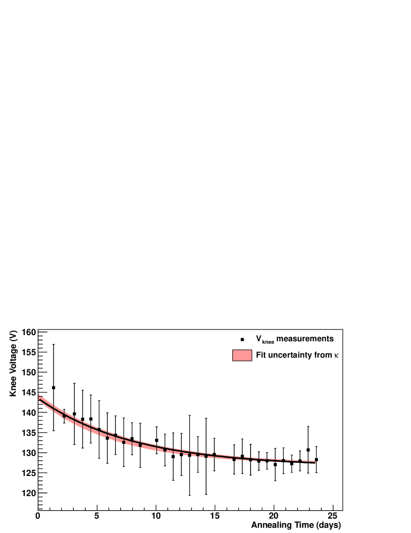
Figure 8 shows the values, associated with fitting the curves over the course of a month, for one of the L00 ladders. To extract an overall time constant, we assume the evolution follows Eq. (9), and we fit for , , and the time constant —we omit the reverse-annealing term proportional to as we observe no increase in at larger values of annealing time. The uncertainties in the values used in the fit are likely correlated between measurements as a function of annealing time. However, as this level of correlation is unknown, we assume them to be uncorrelated, which translates to a larger uncertainty in . The solid line in Fig. 8 corresponds to the best fit using the Eq. (9) parameterization without the reverse-annealing term, resulting in a fitted time constant of days.
Systematic uncertainties due to the self-heating correction are incorporated by varying by its uncertainty in the positive and negative directions, and refitting the -corrected data. The fits corresponding to varying are shown as a red, shaded region in Fig. 8. From these alternate fits, we extract the corresponding time constants and assign the maximum deviation from as the systematic uncertainty on the result. For the L00 ladder shown, the systematic uncertainty is 0.07 days, giving (stat.)(syst.) days. This analysis is repeated for all narrow ladders. A weighted average of the resulting time constants is performed and shown in Sec. 7.
7 Results of the Annealing Study
Figure 9 displays the fitted time constant of the bias current evolution shape for each of the narrow ladders, as described in Sec. 5. The individual results are consistent with a single time constant, suggesting that potential differences among the ladders due to (e.g.) annealing temperature or radiation dose variations are small. The weighted average of days is obtained by assuming uncorrelated statistical uncertainties and fully correlated systematic uncertainties due to the self-heating corrections, as described in A. The total uncertainty on the combined result is indicated with a shaded band.
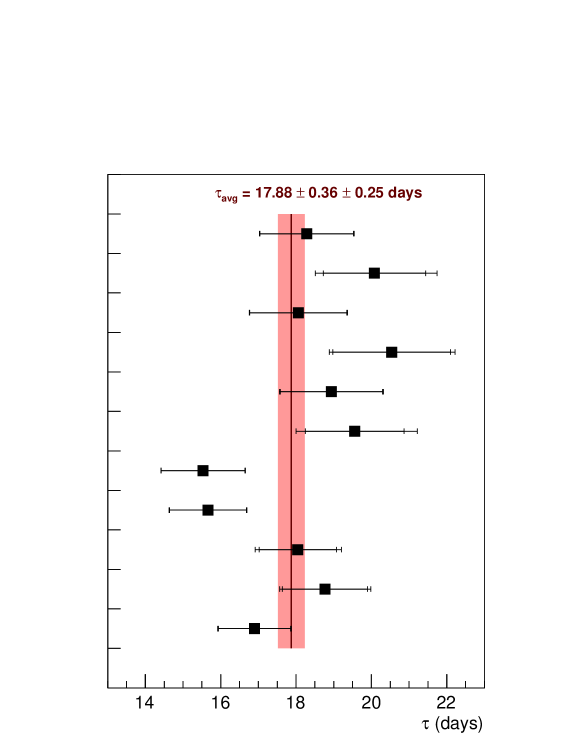
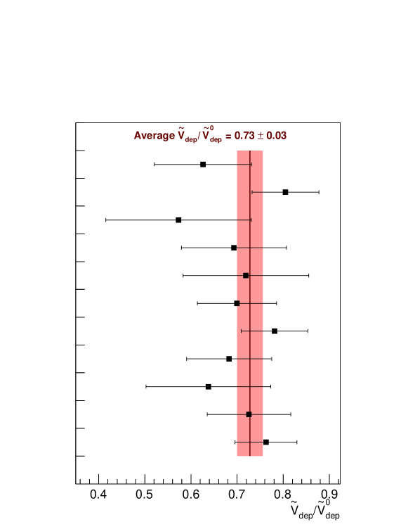
Figure 10 shows the after-before ratio in mapped depletion voltage , as described in Sec. 6.2, for each of the L00 ladders considered as well as a weighted average. The uncertainties of each determination are assumed to be uncorrelated. The average after-before ratio is thus , indicating an average reduction of roughly 25% in due to annealing.
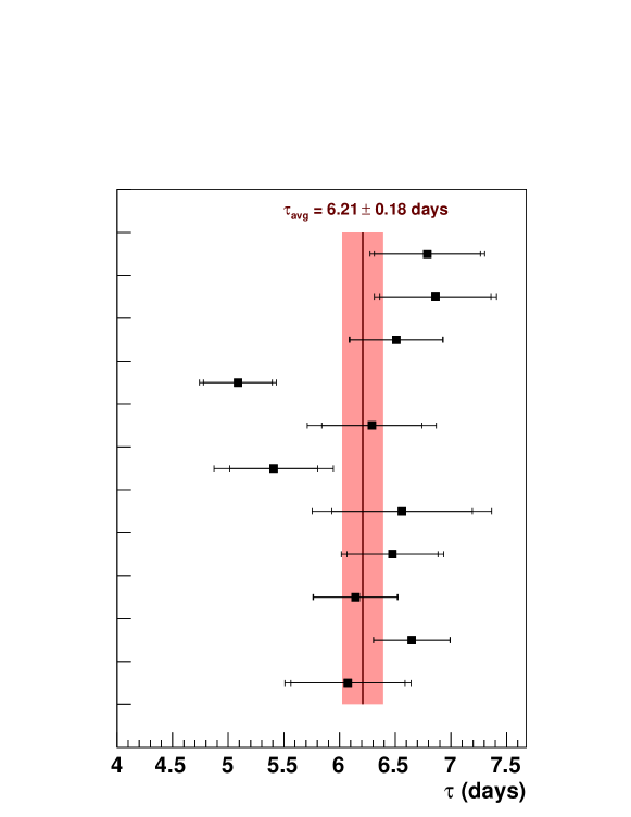
Finally, we present the averaged result for the evolution time constant in Fig. 11, as described in Sec. 6.3. The results is an average of days. The statistical uncertainties are again assumed to be uncorrelated, whereas the systematic uncertainties due to are treated as fully correlated in the weighted average. The solid vertical line and shaded region represent the weighted average and its total uncertainty, respectively.
8 Comparison with the Hamburg Model
In order to compare these measurements with the Hamburg Model, the fraction of annealing that happened during the run must first be estimated using the record of sensor temperatures as a function of time. The temperatures of SVX and L00 sensors during data taking operations were roughly 11 and -2.5, respectively. During shutdowns, with the heat load from the readout chips removed from the system, temperature of both the SVX and L00 sensors was 0-5.
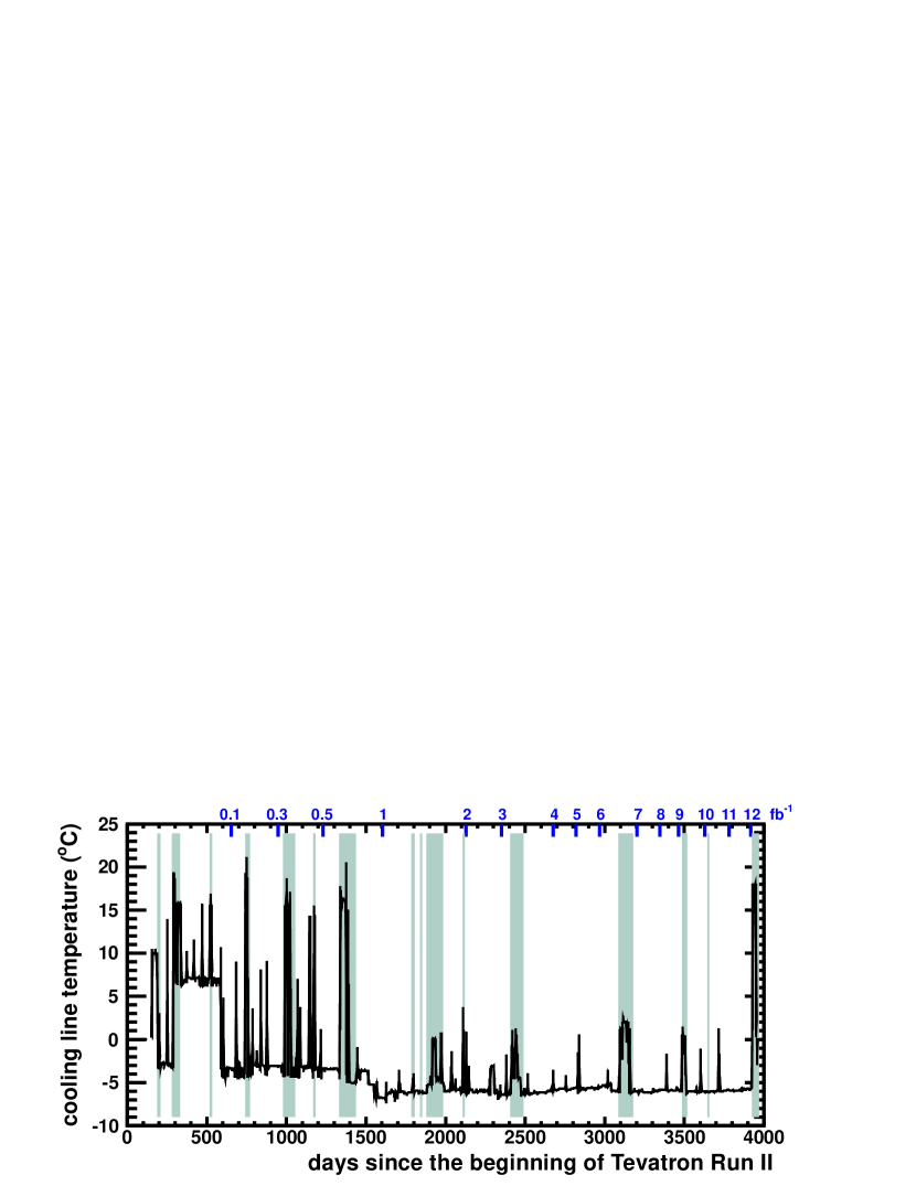
During data-taking operations, the SVX sensors were sufficiently warm that annealing and irradiation happened simultaneously throughout the run. Annealing during shutdown periods was negligible compared with operations for the SVX sensors for both bias current and depletion voltage. The L00 sensors were colder during operations. Figure 12 shows the average measured cooling line temperature for each day as a function of time during the run, with shutdowns indicated with shaded bands. After the first inverse femtobarn of integrated luminosity, the coolant temperature was kept below 5 even during shutdowns. During shutdowns, the sensor temperature was very close to the coolant temperature as the readout chips were not powered and therefore the heat load on the system was significantly reduced. During operations, the sensor temperature is estimated to be 2.5 warmer than the coolant, or -2.5 on average. A few small spikes in the daily average not associated with a shutdown period are visible and result from excursions for a few hours to warmer temperatures during short interruptions in coolant circulation.
8.1 Bias Current Evolution
The total change in bias current expected during the annealing period can be predicted from Eq. (2) and compared to the observed values reported in Fig. 4. The first three terms in Eq. (2) have time constants of 24 minutes, 2.7 hours and 1.0 days at 18, or equivalently 18 hours, 5.0 days, and 46 days at -5, respectively. Thus, the bias current reduction due to annealing represented by the first two terms happened during operations in a continuous fashion for L00. The contribution from the third term is also anticipated to be negligble, considering that less than 10% of the total radiation dose was delivered in the last 90 days of Run II. Considering only the remaining three terms, the measured ratio is expected to be 68% for 24 days of annealing at 18, consistent with the measured values for the L00 sensors. For the SVX sensors, only the last two terms are relevant for the annealing study, and 94% is expected for the ratio , again consistent with the measured values.
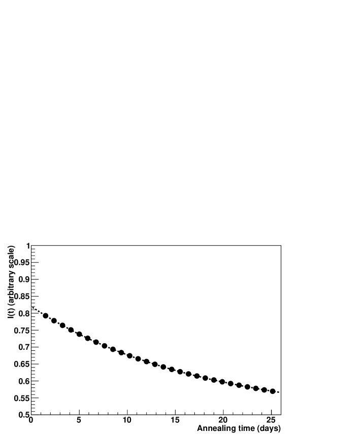
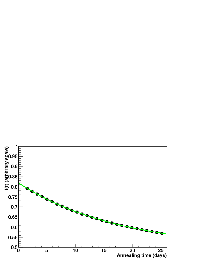
Similarly, we can compare the observed exponential decay of the bias current with model expectations. An experiment was simulated by calculating expected measured currents with a modified version of Eq. (2) for the annealing time patterns of the actual measurements, every 21 hours starting 1.5 days after warmup. Using the considerations of the previous paragraph, Eq. (2) was modified by setting the amplitudes of the first three terms, and equal to 0.
The upper plot of Fig. 13 shows with a dashed line, the expected measured bias currents as a function of annealing time from the modified Eq. (2). In both plots, the circles represent the expected measurements calculated by sampling the dashed line every 21 hours starting at 1.5 days. The solid line in the lower plot is the best fit to the sampled currents using Eq. (3), giving a time constant of 17.58 days, which is in good agreement with the measured value of (stat.)(syst.) days.
8.2 Depletion Voltage Evolution
For the depletion voltage time constant, we expected days. Our measurement of days exceeds this prediction by just over one standard deviation. Due to the complicated dependence on the various model parameters, it is difficult to compare the measured after-before ratio of to the Hamburg model-prediction, which is somewhere between 50% and 65%, as mentioned in Sec. 2. It does appear that our measurement exceeds the Hamburg prediction to some extent, which would be consistent with an assumption that annealing happened to some extent during Run II.
9 Summary
After accumulating 12 fb-1 of integrated luminosity, and being exposed to radiation doses up to 12 Mrad, the CDF Run II silicon detector was annealed at 18 for 24 days. The ratio of the bias currents after the annealing study to that before the study is a measure of how much each subsystem annealed during the run. The overall change and evolution of the bias currents, depletion voltages, and values of several sensors during the annealing process were measured.
For L00, we observed a decrease of the bias current and depletion voltage of the heavily irradiated sensors, with time constants consistent with the Hamburg model expectations. We observed no indication of the reverse annealing on this time scale.
In contrast, the bias currents of SVX changed very little during the annealing period. This confirms that these sensors, with a significantly warmer operating temperature than L00, annealed during data taking. As the operating temperature of the SVX sensors was not directly measured, and the prediction of their temperature from finite element thermal models has large uncertainties, this is an important confirmation of the annealing during the run, which extended the lifetime of the detector.
10 Acknowledgments
The authors would like to thank CDF collborators Dr. J. Nett, Dr. Y.Oksuzian, Dr. I. Redondo for the invaluable assistance in collecting the data presented here and discussing analysis techiques. The authors also thank Dr. A. Junkes (Brown University) for extensive discussions on radiation damage and annealing in silicon detectors. This work would not have been possible without strong support from the CDF operations management and the spokespersons. We also thank the Fermilab staff and the technical staffs of the participating institutions for their vital contributions.
This work was supported by the U.S. Department of Energy and National Science Foundation; the Italian Istituto Nazionale di Fisica Nucleare; the Ministry of Education, Culture, Sports, Science and Technology of Japan; the Natural Sciences and Engineering Research Council of Canada; the National Science Council of the Republic of China; the Swiss National Science Foundation; the A.P. Sloan Foundation; the Bundesministerium für Bildung und Forschung, Germany; the Korean World Class University Program, the National Research Foundation of Korea; the Science and Technology Facilities Council and the Royal Society, UK; the Russian Foundation for Basic Research; the Ministerio de Ciencia e Innovación, and Programa Consolider-Ingenio 2010, Spain; the Slovak R&D Agency; the Academy of Finland; and the Australian Research Council (ARC).
Appendix A Temperature corrections for dissipative heating
The temperature dependence of the bias current for a fully depleted reverse-biased diode is well understood [9]. If the current is measured at a known temperature , then the current at temperature is given by
| (11) |
where is Boltzmann’s constant and eV is the effective band gap energy [11].
The temperature of a biased sensor increases as a result of resistive power dissipation in the sensor, hereafter referred to as “self-heating”. For the scans of the annealing period, this temperature increase was as large as 3 for the L00 narrow sensors at the largest voltages. Such a temperature shift can result in bias current deviations from nominal 18.2 values by as much as 30%. These temperature variations must be removed from a set of measured currents. before information about the annealing processes can be extracted.
The measured currents can be corrected to a common temperature using Eq. (11) if the sensor temperature at the time of the measurement is known. The sensor temperature is not measured directly, however it can be calculated from the measured current at a given bias voltage , assuming that the temperature increases linearly with the power dissipated by the ladder:
| (12) |
where is a proportionality constant.
Using values of determined with a dedicated measurement, a temperature correction was applied to the measured currents before extracting the knee voltage, as shown in Fig. 6, and the time constant of the current decay, shown in Fig. 5.
A.1 Determination of for each sensor
The value of for each sensor was determined by combining data from a dedicated reference current measurement with the last set of scans taken during the annealing period. A collection of reference current measurements were taken at the operating voltage and at half of the operating voltage after the 24-day annealing period. For these measurements, the readout chips were not powered and the measured cooling line temperatures were between -0.5 and 1.1 for the system. Only one sensor was biased at a time to minimize any potential heat load.
The expected bias current at the annealing temperature , in the absence of self heating, can be calculated from the measured reference currents
| (13) |
where is the temperature of the sensor during the measurement of the reference currents.
The last set of scans taken during the annealing period contain bias currents measured in this voltage range. Self heating increases the temperature of the sensor to a value , and the measured current can be corrected to the equivalent current at the annealing temperature by
| (14) |
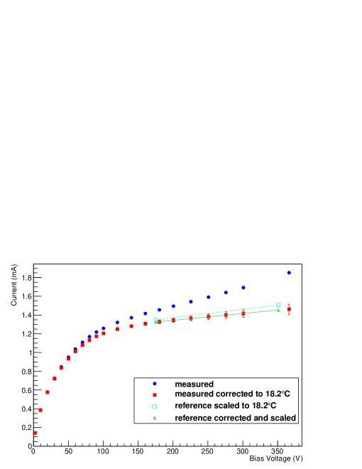
Because there are two reference current measurements at two different bias voltages for each sensor, unique values of and for each sensor are determined by requiring that for both measurements. This initial result is then improved upon iteratively by correcting the reference currents for a small amount of self heating, using the values of and from the previous iteration in Eqs. (12) and (11). For all ladders, the values of and converge in fewer than four iterations. The difference between the initial and final values of is taken as a systematic uncertainty.
Figure 14 illustrates this process for a typical narrow L00 ladder. The measured currents from the scan are shown as solid circles, and the corrected currents as solid squares. The values of and from the first iteration are those for which the solid squares agree with the dashed line, while the final values give agreement with the solid line connecting the corrected reference currents shown with solid triangles. If the bias voltage value of the scan points do not exactly match those of the reference measurement, as in the example illustrated, then the two scan points closest to the reference scan measurements are chosen, and a linear interpolation is used to obtain measured reference currents for those voltages.
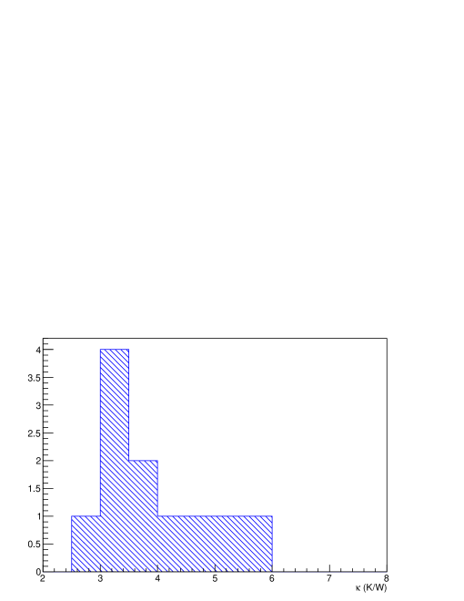
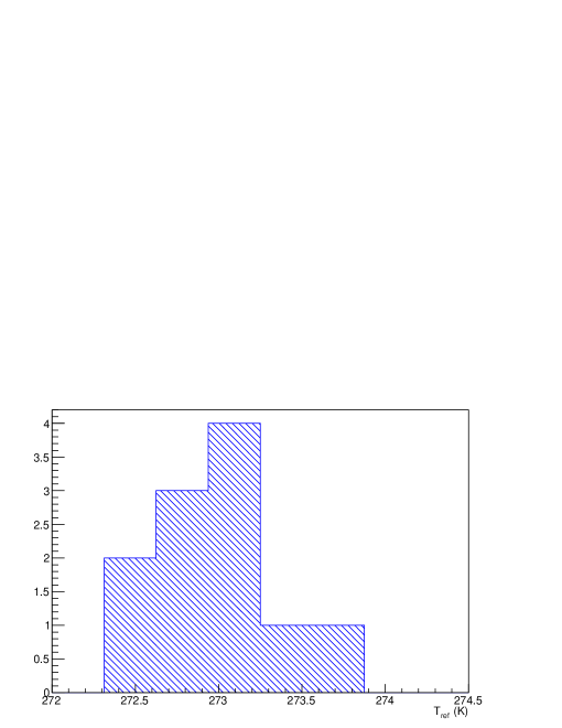
The distributions of and are shown in Figs. 15 and 16. These values are expected to vary slightly with the ladder location and thermal connection to the cooling lines. and have common systematic errors from the uncertainties on the absolute annealing temperature and the effective gap energy eV [11]. For , these two uncertainties combine to give an overall uncertainty of K/W. The time delay between the last warm scan and the reference measurement is different for each ladder, varing from 3 to 24 hours. The current at fixed temperature and voltage decreases due to annealing during this time, but the change is observed to be less than 0.5% for the longest time period and the resulting shifts in and are negligible. An important verification of this self-heating correction method comes from the agreement of the best fit values of with the expectation K derived from the measured cooling line temperatures.
References
- [1] M. Moll, Radiation damage in silicon particle detectors: microscopic defects and macroscopic properties, DESY-THESIS-1999-040 (1999).
- [2] R. Wunstorf, A systematic investigation of the radiation hardness of silicon detectors for high-energy physics experiments, DESY-FH1K-92-01 (1992).
- [3] T. K. Nelson, The CDF Layer 00 detector, Int. J. Mod. Phys. A16S1C 1091-1093 (2001).
- [4] C. S. Hill, Initial experience with the CDF layer 00 silicon detector, Nucl. Instrum. Methods A511 (1-2) 118-120 (2003). Proceedings of the 11th International Workshop on Vertex Detectors.
- [5] CDF Collaboration, SVXII simulation and upgrade proposal, CDF/DOC/SEC_VTX/CDFR/1922 (1992).
- [6] A. Affolder et al, Construction report of the intermediate silicon layers (ISL) ladders, Nucl. Instrum. Meth., Sec. A 461 (1-3) 216-218 (2001). 8th Pisa Meeting on Advanced Detectors.
- [7] Evonik Industries, http://www.rohacell.com
- [8] R.J. Tesarek et al, A measurement of the radiation environment in the CDF tracking volume, Nucl. Instrum. Meth., Sec. A 514 (1-3) 188-192 (2003). Proceedings of the 4th International Conference on Radiation Effects on Semiconductor Materials, Detectors and Devices.
- [9] S. M. Sze, Semiconductor Devices: Physics and Technology, John Wiley & Sons, New York (1985).
- [10] T. Aaltonen et al, Operational Experience, Improvements, and Performance of the CDF Run II Silicon Vertex Detectos, Nucl. Instrum. Meth., Sec. A 729 153-181 (2013).
- [11] A. Chilingarov, Temperature dependence of the current generated in Si, J. Instrum. 8 P1003 (2013).