Determining the stability and activation energy of Si acceptors in AlGaAs using quantum interference in an open hole quantum dot.
Abstract
We fabricated an etched hole quantum dot in a Si-doped (311)A AlGaAs/GaAs heterostructure to study disorder effects via magnetoconductance fluctuations (MCF) at millikelvin temperatures. Recent experiments in electron quantum dots have shown that the MCF is sensitive to the disorder potential created by remote ionised impurities. We utilize this to study the temporal/thermal stability of Si acceptors in -type AlGaAs/GaAs heterostructures. In particular, we use a surface gate to cause charge migration between Si acceptor sites at mK, and detect the ensuing changes in the disorder potential using the MCF. We show that Si acceptors are metastable at mK and that raising the device to a temperature K and returning to mK is sufficient to produce complete decorrelation of the MCF. The same decorrelation occurs at K for electron quantum dots; by comparing with the known trap energy for Si DX centers, we estimate that the shallow acceptor traps in our heterostructures have an activation energy meV. Our method can be used to study charge noise and dopant stability towards optimization of semiconductor materials and devices.
pacs:
73.23.-b, 72.20.-i, 73.63.KvI Introduction
A significant outcome of device miniaturization is the semiconductor quantum dot – a device where electrons or holes are confined in all three spatial dimensions at a length scale comparable to the electron or hole wavelength. These can be made in any semiconductor, in principle, but the -type AlGaAs/GaAs heterostructure is predominant for electrical studies because of the high electron mobilities that can be obtained through growth by molecular beam epitaxy (MBE). Cho (1971); Dingle et al. (1978) Small AlGaAs/GaAs dots isolated by tunnel barriers from source and drain electron reservoirs were used as ‘artificial atoms’ Kastner (1993) for fundamental studies of the physics of few-electron systems, Kouwenhoven et al. (2001) and now play a vital role in the study of electron spin physics Hanson et al. (2007) and the early development of quantum computation architectures. Ladd et al. (2010) Larger AlGaAs/GaAs dots with stronger coupling to the reservoirs have been central to studies of mesoscopic conduction, quantum interference phenomena and electron transport in the quasi-ballistic and ballistic limits, where an electron’s mean-free path is comparable to or exceeds the dot’s confinement width. Lin and Bird (2002); Bird et al. (2003); Micolich et al. (2013)
A hallmark of these larger ‘open’ dots is the appearance of fluctuations in the magnetoconductance at low temperature K, which arise from the Aharonov-Bohm effect. Aharonov and Bohm (1959); Marcus et al. (1992) These fluctuations are reproducible for a given dot on a single measurement cool-down, Marcus et al. (1992) providing a ‘magnetofingerprint’ of the electron trajectories within the dot. Feng et al. (1986) Recent experiments See et al. (2012); Scannell et al. (2012) highlight the important role that the dot geometry, and the remote ionized dopant potential it contains, play in determining these trajectories, even in the ballistic limit. For a single electron dot with fixed geometry, the magnetoconductance fluctuations (MCF) change markedly upon raising the temperature to K briefly and returning to low to remeasure for a modulation-doped AlGaAs/GaAs heterostructure. Scannell et al. (2012) However, for an undoped dot, the MCF remain identical under thermal cycling to temperatures as high as K. See et al. (2012) The change in MCF of the modulation-doped electron dot arises from the spontaneous re-organization of trapped charge in the Si doping layer at K, which alters the dot’s potential landscape. The sensitivity of the MCF to small-angle Coulomb scattering by remote ionized dopants provides a potential new application for semiconductor quantum dots as sensitive detectors of fluctuations in dopant ionization state. See et al. (2012) This could be combined with other methods if needed, e.g., switching noise measurements in quantum point contacts (QPCs), Buizert et al. (2008) to enable studies of how dopants influence the electronic properties of a given device, as we do here, or for optimizing materials growth to obtain devices with high stability and low operating noise. Buizert et al. (2008); Pioro-Ladrière et al. (2005)
Here we demonstrate the potential for investigating the temporal and thermal stability of Si acceptors in a (311)A-oriented Si-doped AlGaAs/GaAs heterostructure using measurements of the MCF in a hole open quantum dot etched into the heterostructure. We do so by utilizing the measured MCF as a magnetofingerprint of the disorder potential generated by a given spatial charge configuration in the partially-ionized acceptor layer. (311)A-oriented Si-doped AlGaAs/GaAs heterostructures are a key materials platform for studying the fundamental physics of low-dimensional hole systems, where the much stronger spin-orbit interaction obtained via the GaAs valence band’s -orbital-like nature gives rise to interesting topological phase Yau et al. (2002) and spin anisotropy Winkler et al. (2000); Danneau et al. (2006); Chen et al. (2010); Klochan et al. (2011); Srinivasan et al. (2013) effects.
A significant problem with (311)A-oriented Si-doped AlGaAs/GaAs heterostructures is the hysteresis/instability that arises when using a surface metal ‘gate’ electrode to electrostatically alter the density of the two-dimensional hole gas (2DHG) formed at a buried AlGaAs/GaAs interface within the heterostructure. Zailer et al. (1994); Daneshvar et al. (1997); Rokhinson et al. (2002) We recently reported that this hysteresis contains two contributions at different time/energy scales: a) surface-state trapping at the gate-heterostructure interface, and b) fluctuations in ionization state of Si dopants. Burke et al. (2012); Carrad et al. (2013) We suggested acceptors dominate the gate hysteresis at K by comparison with higher temperature data in -type (100)-oriented Si-doped AlGaAs/GaAs heterostructures where the surface-state contribution to gate hysteresis is negligible and donor fluctuations cause gate hysteresis. Burke et al. (2012) The hole quantum dot data we present here confirms the low behavior observed for -type devices in Ref. Burke et al. (2012). We show that some fraction of the Si acceptors in Al0.34Ga0.66As act as very shallow trap sites that remain metastable, even at mK. This is in stark contrast to Si donors in Al0.34Ga0.66As where the activation temperature is much greater due to the formation of DX centers, Mooney (1990); Buks et al. (1994) which are donors that can also act as deep, long-lived traps. This capacity allows DX centers to trap charge released by the much shallower ordinary dopants, and gives nanoscale electron quantum devices their high stability at low .
II Methods
The hole quantum dot was fabricated from a -type modulation doped Al0.34Ga0.66As/GaAs heterostructure grown on half of a 2” GaAs (311)A semi-insulating substrate by molecular beam epitaxy (MBE). First, a nm undoped GaAs layer was grown, followed by an undoped, 20-period superlattice with a period of nm GaAs + nm AlAs to trap eventual segregating impurities at its interfaces. The active region was then grown, consisting of nm undoped GaAs, nm undoped Al0.34Ga0.66As spacer, a homogeneously Si-doped nm Al0.34Ga0.66As layer and a nm undoped GaAs cap to prevent oxidation of the Al-content. The Si-doped layer ( = cm-3) provides charge carriers to a high-mobility 2DHG located on the GaAs side of the interface between the undoped Al0.34Ga0.66As layer and the nm GaAs layer. Si was used due to its low diffusion rate compared to Be, and its amphoteric nature, which yields predominantly -type incorporation on the (100)-surface, and -type incorporation on the (311)A-surface.Wang et al. (1985) At room temperature in the dark, we measured a hole density = cm-2 and mobility cm2V-1s-1. At = K we obtained = cm-2 and cm2V-1s-1, corresponding to a large-angle scattering length m. Irradiation with bandgap radiation shows no persistent photoeffect, but lowers the hole density and mobility.
To monitor both the state of our MBE and the doping density in the -type heterostructure, an -type Al0.34Ga0.66As/GaAs heterostructure was grown on a second half of a semi-insulating 2” GaAs (100)-oriented wafer during the same MBE-growth. We obtained an electron density = cm-2 and mobility cm2V-1s-1 at room temperature. In dividing this electron density by the thickness of the Si-doped Al0.34Ga0.66As layer of nm, we obtain the Si-dopant density cm-3 mentioned above, assuming a full activation of the donors and transfer of all electrons into the heterointerface at room temperature. At = K, we measured an electron density cm-2 and mobility cm2V-1s-1 before illumination and cm-2 with cm2V-1s-1 after illumination with bandgap radiation (persistent photo effect). This wafer was also used to verify the expected electrical performance of devices fabricated from this material growth (see Ref.Burke et al. (2012)).
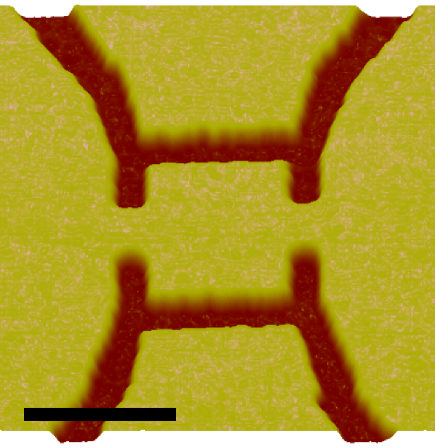
To fabricate the hole quantum dot, a nm high Hall bar mesa was patterned using standard photolithography and wet etching techniques. Photolithographically defined ohmic contacts were formed by thermally evaporating nm of AuBe alloy and annealing at C for s. The m2 quantum dot was defined by electron beam lithography and wet etching with :: H2SO4:H2O2:H2O solution to a trench depth of nm. Figure 1 shows an atomic force micrograph of the resulting dot structure. The dot was covered with a nm thick polyimide insulating layer and an evaporation-deposited nm Ti/ nm Au top gate. A top gate voltage modulates the hole density in the dot and surrounding 2DHG, and also alters the dot’s remote ionized dopant potential, as discussed below. The dot’s electrical conductance was measured using standard four-terminal lock-in techniques with a V excitation voltage at Hz. The current at T ranged between 1 - 15 nA depending on the value of . A Keithley was used to control enabling continuous gate leakage current monitoring; this current was nA throughout the experiment. The device was mounted on a cold finger thermally linked to the mixing chamber of an Oxford Instruments Kelvinox K dilution refrigerator enabling measurements in the temperature range mK K, with two additional points at discrete temperatures of K and K. The device was located inside a superconducting solenoid, enabling a variable magnetic field T to be applied perpendicular to the 2DHG plane.
Our analysis relies on subtractive methods to compare sets of MCF traces. Thus we were careful to ensure each MCF trace was obtained under experimental conditions that were as identical as possible. This included ensuring that all MCF traces were obtained at fixed excitation voltage with the mixing chamber temperature mK, and that MCF traces were only compared if they have the same () to within eh since the dot’s hole density also influences the MCF. Additionally, we deliberately maintain a relatively high excitation voltage to maximise the signal-to-noise ratio of our MCF traces. Together these allow us to attribute changes in MCF solely to changes in acceptor configuration.
III Results
III.1 Temperature dependence of gate characteristics
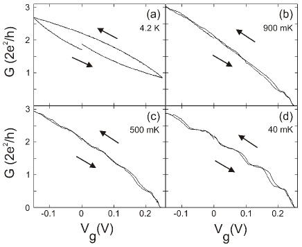
Figure 2 shows how the conductance at zero magnetic field versus evolves as is reduced. Significant hysteresis is observed at K as is first swept to (depletion) and then (accumulation). The anticlockwise hysteresis loop is consistent with Ref. Burke et al. (2012), indicating transport is influenced by gate-induced charge transfer between trap sites located between the gate and 2DHG. The hysteresis reduces as is reduced (Figs. 2(b-d)) due to a reduction in the available thermal energy relative to the trap energy . Conductance quantization develops with reduced ; the plateaus sit at non-integer multiples of due to the non-additivity of QPCs in series separated by less than . Beenakker and van Houten (1989); Kouwenhoven et al. (1989)
A noteworthy aspect is that the charge migration/hysteresis means our devices’ electrical characteristics evolve with both time and experimental parameter history. Thus Fig. 2 should be considered only as a ‘snapshot’ of the device at that time. In particular, readers should be cautious in using Fig. 2(d) to map to for Figures 3-5, as the versus characteristic offsets horizontally depending on device parameter history. To deal with this, we returned to particular values where quantized conductance plateaus occur to compare MCF, rather than comparing MCF at a specific . Simply returning to a given results in much larger changes in and the MCF than in Figures 3-5.
III.2 Temporal stability of the MCF
The hysteresis in Fig. 2(d) indicates some charge between the gate and 2DHG remains mobile even at mK. The first question, by necessity, is the timescale over which the charge configuration remains stable at fixed and minimum . This is essential to knowing whether provides a meaningful quasi-static magnetofingerprint of transport on the timescale for obtaining a trace, typically min, and that obeys known behaviors e.g., the Onsager-Casimir symmetry relation . Onsager (1931); Casimir (1945) Note that the defined dot geometry is fixed, so MCF changes at fixed directly reflect changes in the dot’s underlying disorder potential. See et al. (2012); Scannell et al. (2012)
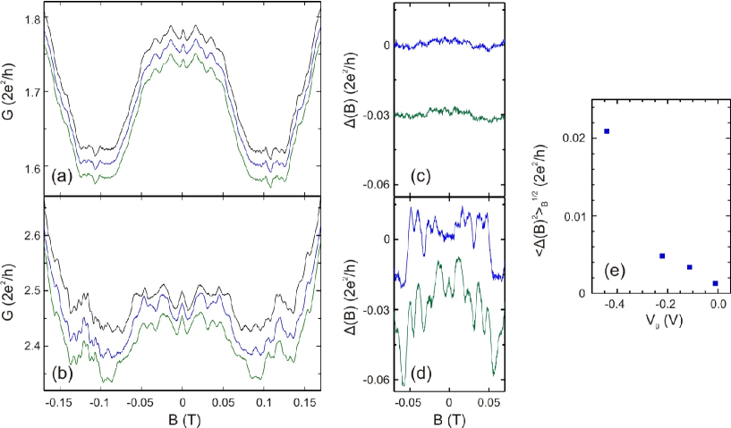
Figures 3(a/b) show how evolves at fixed , with traces at times (black), (blue) and hours (green) after setting mV and mV to give (a) and (b) , respectively. We obtain almost identical MCF at , and hrs with mV (Fig. 3(a)), but MCF evolves markedly over time with mV (Fig. 3(b)), indicative of significant disorder potential changes within the dot. See et al. (2012); Scannell et al. (2012) To highlight this, Figures 3(c/d) present the conductance difference where for or hours. The subtraction of removes any background d.c. conductance offset due to changes in trapped charge outside the dot/QPCs and more than a coherence length away. This offset is not always gradual; random ‘jumps’ to higher/lower occur every few hours. One example occurred between the top and middle traces in Fig. 3(a), removing the need for a vertical offset for the blue trace. Thus, changes in show up in as fluctuations around .
Fig. 3(c) shows that remains close to for all with mV, as expected for almost identical traces. Conversely, substantial fluctuations emerge for mV (Fig. 3(d)), with the magnitude of the fluctuations increasing with time. The marked changes to disorder potential at more negative suggests the gate electric field drives this underlying change in disorder potential. One possible scenario is: cooling the device at sets an initial equilibrium state for trapped charge in the Si acceptor layer. The equilibrium bandstructure in this finite thickness layer is such that the occupied trap density in the growth direction is inhomogeneous; this picture is consistent with observations for the deep-trapping Si DX center in (100)-oriented AlGaAs/GaAs heterostructures, Pioro-Ladrière et al. (2005); Buks et al. (1994) albeit with shallower traps here. A non-zero produces an electric field along that drives charge migration between trap sites. If then the migration rate is slow and should increase with the difference between and its value during cool-down (i.e., ).
To test this scenario, we took pairs of traces separated by hr, starting at V and using progressively more negative . To quantify MCF differences, i.e., the magnitude of fluctuations, we plot the root-mean-square conductance difference versus in Figure 3(e). The quantity is similar to the correlation used previously, See et al. (2012); Scannell et al. (2012); Taylor et al. (1997) and differs only by the absence of a normalization coefficient based on random traces. Taylor et al. (1997) For completeness, corresponding values are shown in the Appendix. Fig. 3(e) shows a clear increase in with more negative , consistent with gate field driven charge migration in the Si acceptor layer.
III.3 Evolution of MCF with gate modulation
Figure 3(e) naturally leads to the question: How robust is the MCF if is swept to some distant value and returned to its original setting? In other words, to what extent does charge migration in produce changes in charge distribution in the plane, i.e., ionized dopant potential? This will be linked to trap site population – if traps are mostly filled, charge may migrate in and ultimately return to the same initial trap site under a cyclic variation in ; if they are mostly empty, the probability of return will be low.
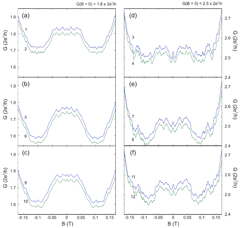
Figure 4 shows pairs of traces obtained alternately at the and plateaus. Two traces were taken at each gate voltage to directly compare the temporal stability to disorder induced by the gate potential over a similar time scale: The numbers in Fig. 4 indicate the sequence in which traces were obtained. The left (right) column in Fig. 4 should be considered as a cyclic variation from to and back; as such we do this experiment twice, once starting at more positive and cycling to more negative (left column), and once vice versa (right column). If cyclic variation produced no change in the dot’s disorder potential, we would expect six identical traces at , and a different set of six identical traces at ; the difference in between the and plateaus is caused by the underlying difference in hole density. Inspection of Fig. 4 makes it clear the disorder potential changes with cyclic variation in . Specifically, varies more between panels than within each panel, suggesting that cyclic variation in produces stronger changes than background temporal changes.
To confirm this, we again used to quantify the changes: Pairs of traces in each panel give an average of ( for the left (right) column of Fig. 4. In contrast, if we compare the second traces in a/b, b/c and a/c (or d/e, e/f and d/f) we get an average of (. The values relating to cyclic variation are larger than those relating to temporal changes: this confirms that significant changes in dot disorder potential result from cyclic variation in . The fact that the MCF continues to evolve through the 6 cycles also suggests that the trap site population is low in this sample. This is not surprising, as the primary purpose of the dopant charge is to populate the 2DHG and quantum dot.
III.4 Evolution of MCF with thermal cycling
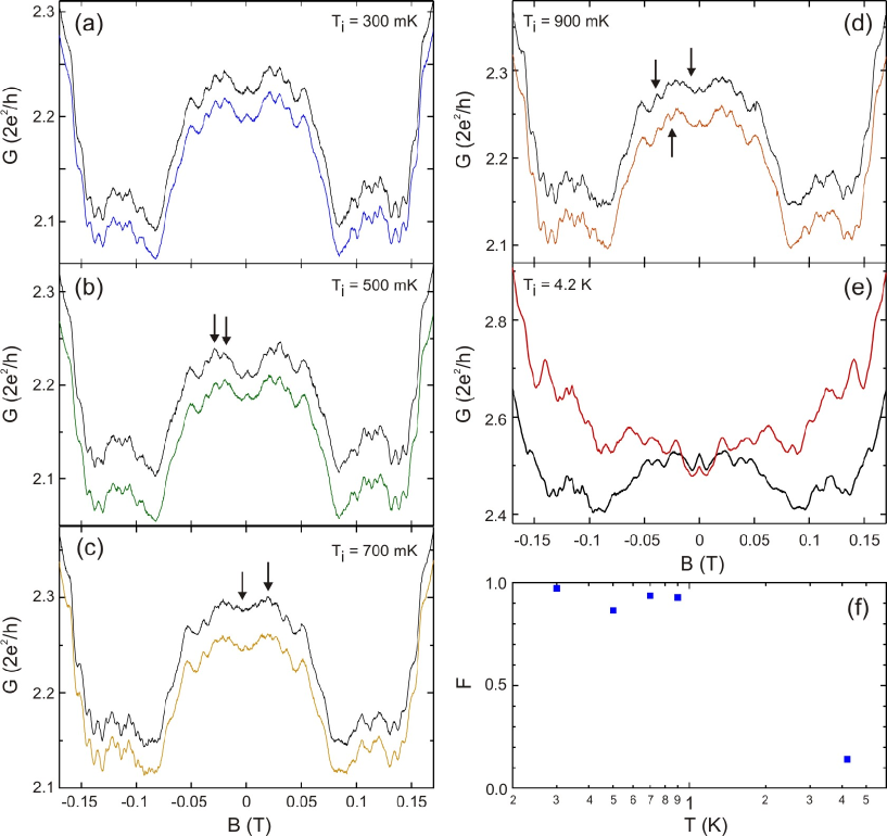
The previous two sections showed that at mK, charge migration occurs between some proportion of Si acceptors in the AlGaAs layer under the influence of an electric field, but spontaneous re-organization does not occur. This suggests a metastable configuration: i.e., the thermal energy at mK is slightly lower than the activation energy for the Si acceptors. We thus attempted to determine via temperature studies of . The probability of trap deoccupation depends on relative to , thus elevating should lead to more rapid changes in disorder potential and thereby in , reflected by increased . Scannell et al. Scannell et al. (2012) recently performed such a study for GaAs and InGaAs electron quantum dots using the following methodology: Set and hold a particular , obtain at base temperature mK, heat to mK for some time , return to and remeasure , heat to for , return to and remeasure , repeat times until K. The at each iteration is then compared to the initial trace, with the correlation , where is a normalization factor, plotted against to identify where becomes sufficient to cause major changes to . Scannell et al. (2012)
Repeating the study by Scannell et al. for a hole quantum dot, as we do here, faces two serious challenges. The higher effective mass for holes results in a significantly reduced phase coherence time relative to electrons. Faniel et al. (2007) As a result must be measured at lower to obtain MCF; the MCF of our device is quenched at mK. This means our measurements require a dilution refrigerator, where the available range is limited to mK, K and K. In contrast, the 3He system used in Ref. Scannell et al. (2012) allows continuous, precise variation of over the range mK K. The second challenge is that is much smaller for our system. This means that even if we had good control over above mK, much of this range is of limited use as we should reach the point where saturates at its maximum value at relatively low . Nonetheless, we attempt the study within these limitations to confirm at least that for Si acceptors in (311)A AlGaAs/GaAs heterostructures is much smaller than for Si donors in (100) AlGaAs/GaAs heterostructures.
Figure 5 shows traces obtained before and after cycling to and K. We first make one important note regarding interpretation relative to Ref. Scannell et al. (2012); here we compare the traces obtained immediately before/after cycling to , rather than comparing after to a common, initial ‘’ trace. This is to more fairly deal with the continuous temporal evolution/relaxation in ; i.e., we do not want our analysis to include the temporal changes in observed in Fig. 3. The MCF in Fig. 5(a) shows little change after thermal cycling to mK. For this pair of traces we obtain a correlation . As we increase in steps of mK in Fig. 5(b-d), the differences between MCF traces before and after cycling to begin to increase, as indicated by the arrows. Correspondingly, there is a gradual fall-off in towards , evident in Fig. 5(f) where we plot versus . There is a little scatter in for mK, but this is also apparent in Ref. Scannell et al. (2012), and often results from small, slow background variations running through the data. Ultimately, upon reaching mK, has not dropped off markedly.
While the data in Fig. 5(a-d) could be obtained at fixed , with controllably increased to , held there for min and then returned to mK for measurement, this is not possible for the next available K. More effort is needed to reach K with a dilution refrigerator, i.e., remove of 3He/4He mixture, add exchange gas, equilibrate with K bath, pump out exchange gas, recondense mixture and restart circulation; this process takes many hours. Additionally, the resulting dopant reorganization inevitably means that does not occur at the same . Indeed, the initial and final traces in Fig. 5(e) were obtained at and V, respectively. They are markedly different, and the corresponding .
Fig. 5(f) shows that the where the MCF decorrelates rapidly lies somewhere in the range K. The rapid drop-off for an AlGaAs/GaAs electron dot in Ref. Scannell et al. (2012) occurs at K. If we estimate that K for in Fig. 5(f), then we would expect the trap depth for our Si acceptors to be of that for Si donors. Assuming the Si donors are DX centers with depth meV, Mooney (1990) then we can estimate the shallow Si acceptor trap depth for our dots to be meV. The isolated Si acceptor energy in GaAs is meV Kirkman et al. (1978) and meV in AlGaAs Galbiati et al. (1996); our trap is over an order of magnitude smaller. This value of meV should be considered a lower bound estimate as the difficulties involved in obtaining the K measurement could have reduced the measured . However, even if the decorrelation temperature were as high as K, the corresponding meV would still be smaller than the isolated Si-acceptor level in AlGaAs. One possible source of this small trap is the Si-X acceptor defect, Murray et al. (1989) which appears at very high Si doping densities. As Ashwin et al. point out, Si-X would need a small activation energy to be electrically active amongst a high density of isolated Si acceptors. Ashwin et al. (1994)
IV Conclusions
We have used the sensitivity of the magnetoconductance fluctuations in an open quantum dot to small-angle scattering from remote ionized impurities See et al. (2012); Scannell et al. (2012) to study the stability of Si acceptors in (311)A AlGaAs/GaAs heterostructures. With mK and , the MCF remain reproducible for a period hrs, demonstrating that under the simplest quasi-static conditions, a hole quantum dot can show stable, meaningful electrical characteristics and MCF, consistent with previous studies. Faniel et al. (2007) By contrast, the temporal stability of the MCF is significantly reduced as is made more negative. Similarly, MCF changes are observed when cycling away from some initial value, and returning to a value that gives the same . We attribute this to migration of charge between trap sites in the Si acceptor layer due to the electric field induced between the gate and 2DHG by . These results suggest a metastable state for Si acceptors in AlGaAs at mK, with the activation energy of acceptors larger than the thermal energy . To determine , we followed Scannell et al. and looked at how periods at higher temperatures changed the MCF at fixed . This experiment faced many difficulties, but we found that a K is sufficient to produce complete decorrelation of the MCF. By comparing with the known trap energy for Si DX centers and the required to produce decorrelation in electron devices, we estimate that the shallow acceptor traps in our heterostructures have an activation energy meV, consistent with our earlier studies of device hysteresis. Burke et al. (2012) This work demonstrates the capacity for the MCF in quantum dots to be used as a tool for detecting temporal changes in ionized dopant configuration and charge trap occupation in semiconductor heterostructures. One structure of immediate interest is C-doped -type AlGaAs/GaAs heterostructures, since devices fabricated from this material also exhibit gate instability at low temperature. Csontos et al. (2010) Repeating the experiments conducted here for this material could help to determine whether charge migration between C acceptors plays a role in this instability, and determine the C acceptor activation energy in AlGaAs.
Acknowledgements.
This work was funded by Australian Research Council Grants DP0110103802, FT0990285, DP120101859, DP120102888 and by the Australian Government under the Australia-India Strategic Research Fund. DR and ADW acknowledge support from DFG SPP1285 and BMBF QuaHL-Rep 16BQ1035. This work was performed in part using the NSW node of the Australian National Fabrication Facility (ANFF). We thank L. Eaves for helpful discussions on donors and acceptors in AlGaAs/GaAs heterostructures.*
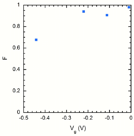
Appendix A Correlation data for Figure 3(e)
Figure 6 shows the correlation versus gate voltage corresponding to the data presented in Figure 3(e). The correlation is obtained by applying a cross-correlation analysis to a pair of traces and :
| (1) | |||||
| (2) |
The symbol represents an average over the data points spanning , where T is the field at which the cyclotron diameter matches the billiard width. The normalization constant is calculated by averaging the correlations of pairs of randomly generated traces with the same average, maximum and minimum as the two analysed traces and . Adopting this normalization, the correlation scale varies between 1 for mathematically identical traces to 0 for complete decorrelation. Further details of this method can be found in Refs. Taylor et al. (1997); See et al. (2012); Scannell et al. (2012).
References
- Cho (1971) A. Y. Cho, Appl. Phys. Lett. 19, 467 (1971).
- Dingle et al. (1978) R. Dingle, H. L. Stormer, A. C. Gossard, and W. Wiegmann, Applied Physics Letters 33, 665 (1978).
- Kastner (1993) M. A. Kastner, Phys. Today 46, 24 (1993).
- Kouwenhoven et al. (2001) L. P. Kouwenhoven, D. G. Austing, and S. Tarucha, Rep. Prog. Phys. 64, 701 (2001).
- Hanson et al. (2007) R. Hanson, L. P. Kouwenhoven, J. R. Petta, S. Tarucha, and L. M. K. Vandersypen, Rev. Mod. Phys. 79, 1217 (2007).
- Ladd et al. (2010) T. D. Ladd, F. Jelezko, R. Laflamme, Y. Nakamura, C. Monroe, and J. L. O’Brien, Nature 464, 45 (2010).
- Lin and Bird (2002) J. J. Lin and J. P. Bird, J. Phys.: Condens. Matter 14, R501 (2002).
- Bird et al. (2003) J. P. Bird, R. Akis, D. K. Ferry, A. P. S. de Moura, Y.-C. Lai, and K. M. Indlekofer, Rep. Prog. Phys. 66, 583 (2003).
- Micolich et al. (2013) A. P. Micolich, A. M. See, B. C. Scannell, C. A. Marlow, T. P. Martin, I. Pilgrim, A. R. Hamilton, H. Linke, and R. P. Taylor, Fortschritte der Physik 61, 332 (2013).
- Aharonov and Bohm (1959) Y. Aharonov and D. Bohm, Phys. Rev. 115, 485 (1959).
- Marcus et al. (1992) C. M. Marcus, A. J. Rimberg, R. M. Westervelt, P. F. Hopkins, and A. C. Gossard, Phys. Rev. Lett. 69, 506 (1992).
- Feng et al. (1986) S. Feng, P. A. Lee, and A. D. Stone, Phys. Rev. Lett. 56, 1960 (1986).
- See et al. (2012) A. M. See, I. Pilgrim, B. C. Scannell, R. D. Montgomery, O. Klochan, A. M. Burke, M. Aagesen, P. E. Lindelof, I. Farrer, D. A. Ritchie, R. P. Taylor, A. R. Hamilton, and A. P. Micolich, Phys. Rev. Lett. 108, 196807 (2012).
- Scannell et al. (2012) B. C. Scannell, I. Pilgrim, A. M. See, R. D. Montgomery, P. K. Morse, M. S. Fairbanks, C. A. Marlow, H. Linke, I. Farrer, D. A. Ritchie, A. R. Hamilton, A. P. Micolich, L. Eaves, and R. P. Taylor, Phys. Rev. B 85, 195319 (2012).
- Buizert et al. (2008) C. Buizert, F. H. L. Koppens, M. Pioro-Ladrière, H.-P. Tranitz, I. T. Vink, S. Tarucha, W. Wegscheider, and L. M. K. Vandersypen, Phys. Rev. Lett. 101, 226603 (2008).
- Pioro-Ladrière et al. (2005) M. Pioro-Ladrière, J. H. Davies, A. R. Long, A. S. Sachrajda, L. Gaudreau, P. Zawadzki, J. Lapointe, J. Gupta, Z. Wasilewski, and S. Studenikin, Phys. Rev. B 72, 115331 (2005).
- Yau et al. (2002) J.-B. Yau, E. P. De Poortere, and M. Shayegan, Phys. Rev. Lett. 88, 146801 (2002).
- Winkler et al. (2000) R. Winkler, S. J. Papadakis, E. P. DePoortere, and M. Shayegan, Phys. Rev. Lett 85, 4574 (2000).
- Danneau et al. (2006) R. Danneau, O. Klochan, W. R. Clarke, L. H. Ho, A. P. Micolich, M. Y. Simmons, A. R. Hamilton, M. Pepper, D. A. Ritchie, and U. Zülicke, Phys. Rev. Lett. 97, 026403 (2006).
- Chen et al. (2010) J. C. H. Chen, O. Klochan, A. P. Micolich, A. R. Hamilton, T. P. Martin, L. H. Ho, U. Zülicke, D. Reuter, and A. D. Wieck, New J. Phys 12, 033043 (2010).
- Klochan et al. (2011) O. Klochan, A. P. Micolich, A. R. Hamilton, K. Trunov, D. Reuter, and A. D. Wieck, Phys. Rev. Lett. 107, 076805 (2011).
- Srinivasan et al. (2013) A. Srinivasan, L. A. Yeoh, O. Klochan, T. P. Martin, J. C. H. Chen, A. P. Micolich, A. R. Hamilton, D. Reuter, and A. D. Wieck, Nano Lett. 13, 148 (2013).
- Zailer et al. (1994) I. Zailer, J. E. F. Frost, C. J. B. Ford, M. Pepper, M. Y. Simmons, D. A. Ritchie, J. T. Nicholls, and G. A. C. Jones, Phys. Rev. B 49, 5101 (1994).
- Daneshvar et al. (1997) A. J. Daneshvar, C. J. B. Ford, A. R. Hamilton, M. Y. Simmons, M. Pepper, and D. A. Ritchie, Phys. Rev. B 55, 13409 (1997).
- Rokhinson et al. (2002) L. P. Rokhinson, D. C. Tsui, L. N. Pfeiffer, and K. W. West, Superlatt. Microstruct. 32, 99 (2002).
- Burke et al. (2012) A. M. Burke, D. E. J. Waddington, D. J. Carrad, R. W. Lyttleton, H. H. Tan, P. J. Reece, O. Klochan, A. R. Hamilton, A. Rai, D. Reuter, A. D. Wieck, and A. P. Micolich, Phys. Rev. B 86, 165309 (2012).
- Carrad et al. (2013) D. J. Carrad, A. M. Burke, P. J. Reece, R. W. Lyttleton, D. E. J. Waddington, A. Rai, D. Reuter, A. D. Wieck, and A. P. Micolich, J. Phys.: Condens. Matter 25, 325304 (2013).
- Mooney (1990) P. M. Mooney, J. Appl. Phys 67, R1 (1990).
- Buks et al. (1994) E. Buks, M. Heiblum, Y. Levinson, and H. Shtrikman, Semicond. Sci. Technol. 9, 2031 (1994).
- Wang et al. (1985) W. I. Wang, E. E. Mendez, T. S. Kuan, and L. Esaki, Applied Physics Letters 47 (1985).
- Beenakker and van Houten (1989) C. W. J. Beenakker and H. van Houten, Phys. Rev. B 39, 10445 (1989).
- Kouwenhoven et al. (1989) L. P. Kouwenhoven, B. J. van Wees, W. Kool, C. J. P. M. Harmans, A. A. M. Staring, and C. T. Foxon, Phys. Rev. B 40, 8083 (1989).
- Onsager (1931) L. Onsager, Phys. Rev. 38, 2265 (1931).
- Casimir (1945) H. B. G. Casimir, Rev. Mod. Phys. 17, 343 (1945).
- Taylor et al. (1997) R. P. Taylor, A. P. Micolich, R. Newbury, and T. M. Fromhold, Phys. Rev. B 56, R12733 (1997).
- Faniel et al. (2007) S. Faniel, B. Hackens, A. Vlad, L. Moldovan, C. Gustin, B. Habib, S. Melinte, M. Shayegan, and V. Bayot, Phys. Rev. B 75, 193310 (2007).
- Kirkman et al. (1978) R. F. Kirkman, R. A. Stradling, and P. J. Lin-Chung, J. Phys. C 11, 419 (1978).
- Galbiati et al. (1996) N. Galbiati, E. Grilli, M. Guzzi, L. Brusaferri, L. Pavesi, and M. Henini, Semiconductor Science and Technology 11, 1830 (1996).
- Murray et al. (1989) R. Murray, R. C. Newman, M. J. L. Sangster, R. B. Beall, J. J. Harris, P. J. Wright, J. Wagner, and M. Ramsteiner, J. Appl. Phys. 66, 2589 (1989).
- Ashwin et al. (1994) M. J. Ashwin, M. R. Fahy, R. C. Newman, J. Wagner, D. A. Robbie, M. J. L. Sangster, I. Siller, E. Bauser, W. Braun, and K. Ploog, J. Appl. Phys. 76, 7839 (1994).
- Csontos et al. (2010) M. Csontos, Y. Komijani, I. Shorubalko, K. Ensslin, D. Reuter, and A. D. Wieck, Applied Physics Letters 97, 022110 (2010).