Electronic structure at nanocontacts of surface passivated CdSe nanorods with gold clusters
Abstract
We report the effects of variation in length on the electronic structure of CdSe nanorods derived from atomic clusters and passivated by fictitious hydrogen atoms. These nanorods are augmented by attaching gold clusters at both the ends to form a nanodumbbell. The goal is to assess the changes at nanolevel after formation of contacts with gold clusters serving as electrodes and compare the results with experimental observations Steiner et al. (2005). Calculations involving nanorods of length 4.6 Å to 116.6 Å are performed using density functional theory implemented within plane-wave basis set. The binding energy per atom saturates for nanorod of length 116.6 Å. It is interesting to note that upon attaching gold clusters, the nanorods shorter than 27 Å develop metallicity by means of metal induced gap states (MIGS). Longer nanorods exhibit a nanoscale Schottky barrier emerging at the center. For these nanorods, interfacial region closest to the gold electrodes shows a finite density of states in the gap due to MIGS, which gradually decreases towards the center of the nanorod opening up a finite gap. Bader charge analysis indicates localized charge transfer from metal to semiconductor.
pacs:
73.20At, 73.21.Hb, 73.30.+y, 73.40.SxI Introduction
Group II-VI semiconductors possess an ionic character which leads to larger
band gaps (BGs) and highly coordinated structures in bulk. This property
differentiates them from other compound semiconductors in terms of size and
structure dependent aspects at nanoscale. CdSe being the most popular amongst
them, due to the reproducibility of its optical absorption and emission
properties, has potential applications such as biosensors Chan and Nie (1998), displays
Colvin et al. (1994) and quantum dot lasers Klimov (2000). Due to the unique polar axis of
hexagonal wurtzite geometry of these semiconductors, these structures often
form more anisotropic shapes Manna et al. (2000). These higher aspect ratio polymorphs,
which lead to highly polarised emission, have many applications in
optoelectronics Empedocles et al. (1999). Current synthesis techniques even allow for the
diversity of geometric structures such as nanowires, nanobelts, nanotubes and
nanorods. In particular, one dimensional structures like nanorods have shown to
support a high density of excitons and offer the possibility of enhanced
transport of dissociated charge carriers. Shape-controlled synthesis for CdSe
nanorods has been reported in last decade Hu et al. (2001); Peng (2003); Barnard et al. (2006).
Metal-semiconductor (M-S) interfaces and nanostructured systems are also
gathering interest among the science community Steiner et al. (2005); de Paiva and Felice (2008); Mokari et al. (2005); Salant et al. (2006); Costi et al. (2008) due to their potential applications in developing electronic and
optoelectronic devices. The space-charge region in bulk M-S interfaces extends
upto few nanometers. It is therefore fascinating to study nanostructures which
physically are even less than few nanometers. The electronic properties of
nanoscale counterpart of bulk M-S interfaces are yet to be understood
completely. From the technological point of view, understanding the properties
of such nanocontacts is a major step in the route towards the implementation of
semiconductor nanocrystals (as well as molecules) in nanoelectronic device
architectures. With the aim of finding answers to the specific issues
pertaining to nanoelectronic device architectures, Landman et al studied the M-S
nanojunction problem theoretically Landman et al. (2000). They showed induction of subgap
states near the Si-Al interface, decaying in Si nanowire and development of
relatively large Schottky barriers in comparison to bulk. Demechenko and Wang
calculated electronic structure of CdSe nanowires, in contact with metallic
electrodes of experimentally relevant sizes, by incorporating the electrostatic
image potential in atomistic single particle Schrödinger equation Demechenko and Wang (2007).
They demonstrated strong nanowire-size-dependence of localized electron-hole
states induced by the electrode.
In a scanning tunneling spectroscopy study of gold-tipped CdSe nanorods
(nanodumbbell), Steiner et al observed a gap similar to that in bare CdSe
nanorods near the nanodumbbell center, while subgap structure is found near the
M-S nanocontact Steiner et al. (2005). They attributed this behaviour to the formation of
subgap interface states that vanished rapidly towards the center of the rod,
consistent with theoretical predictions given by Landman et al Landman et al. (2000).
These states lead also to modified Coulomb staircase and in some cases to
negative differential conductance on the gold tips. The tunneling spectra can
be correlated with the theoretical calculation of density of states (DOS).
Theoretical predictions regarding range for decay of metal induced subgap
states is about 1 nm Landman et al. (2000) whereas experiments indicate that the subgap
states exist even up to 5 nm from the interface Steiner et al. (2005). The experimental
estimates are dictated by spatial resolution and the fact that locality of
tunneling spectra holds up to approximately the exciton-Bohr radius of material
Steiner et al. (2005) ( 5.6 nm for CdSe Meulenberg et al. (2009)). Present work is motivated by
this experimental work of Steiner et al.
In present work, we study passivated CdSe nanorods of various lengths in order
to see the effect of length variation on charge density profile of the rods. We
also study their density of states profile upon formation of nanocontacts with
gold clusters. We found that our results are qualitatively similar to those of
Landman et al Landman et al. (2000) and Steiner et al Steiner et al. (2005).
II Computational details
Our calculations are based on density functional theory, implemented through
Vienna Ab-initio Simulations Package Kresse and Furthmuller (1996) and are performed employing
plane augmented wave Blochl (1994) with exchange-correlation energy functional as
given by Perdew, Burke and Ernzerhof Perdew et al. (1996). The valence electronic
configurations for Cd, Se and Au atoms are, , and
respectively. The cut-off energy used in plane wave expansion
is 274.34 eV. The self-consistent convergence of energy is set to 10-5 eV.
The calculations are performed only at a single -point, namely the center
of the Brillouin zone. Occupation numbers are treated according to the
Fermi-Dirac scheme with a broadening of 0.001 eV. A sufficiently large unit
cell is chosen for the free standing CdSe nanorods so that the minimum distance
from the cluster boundary to unit cell boundary was 5 Å in each direction.
This vacuum region is even larger (7 Å) for gold attached CdSe nanorods.
To understand the structural stability, lattice-dynamical calculations
(resulting in phonon DOS) are performed within the framework of self-consistent
density functional perturbation theory. Force constant matrices thus obtained
are used to generate vibrational frequencies of the system. In order to analyse
the bonding between gold cluster and CdSe nanorods, Bader charge analysis
method is used based on the algorithm developed by Henkelman et al
Tang et al. (2009); Sanville et al. (2007); Henkelman et al. (2006).
III Results and Discussions
III.1 Cluster derived CdSe nanorods
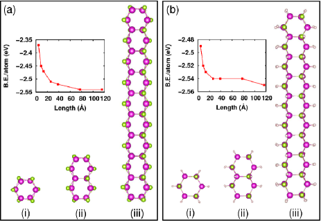
The nanorods are generated by relaxing a fragment (viz. Cd3Se3) of bulk
wurtzite structure of CdSe crystal in direction, into its
global minimum. This fragment has planar structure and can be considered as the
basic building block of the longer nanorods (CdnSen). In this cluster, Cd
atoms form an equilateral triangle of side 3.22 Å and Cd-Se bond length is
2.51 Å. Further, Cd6Se6 nanorod is constructed by stacking these six
atom rings in chair conformation (See Figure 1-a(ii)). This is the
smallest nanorod under consideration. The atoms in this geometry relax in such
a manner that intraplanar Cd-Se bond lengths are optimized to 2.60 Å, and
Cd-Se interplanar bond lengths become 2.82 Å. The length of this nanorod is
found to be 4.34 Å. The longer nanorods are then constructed as the growth
over Cd6Se6 cluster and can be viewed as “n” Cd6Se6 clusters
coupled together sharing a Cd2Se2 in common (See Figure 1).
Thus, we are dealing with the structures where all the atoms reside on the
surface. Binding energy (BE) (defined as the difference between total energies
of nanorods and the constituent atoms) indicate that structure is stable. As
shown by the graph in the inset of Fig. 1(a), BE per atom reduces
initially with the length of the nanorod and then saturates (See also Table
1). At smaller lengths of the nanorods, the structures are more or
less spherical. But as the length increases the aspect ratio increases, thus
making the BE per atom constant.
| Structures | Length (Å) | Band gap | BE per | |||
|---|---|---|---|---|---|---|
| (eV) | atom (eV) | |||||
| Bare | +H* | Bare | +H* | Bare | +H* | |
| Cd6Se6 | 4.34 | 4.64 | 2.02 | 3.17 | -2.37 | -2.49 |
| Cd10Se10 | 8.65 | 9.04 | 1.98 | 2.99 | -2.45 | -2.52 |
| Cd14Se14 | 12.91 | 13.50 | 2.03 | 2.94 | -2.47 | -2.53 |
| Cd26Se26 | 25.76 | 26.60 | 1.99 | 2.71 | -2.51 | -2.54 |
| Cd38Se38 | 38.55 | 39.43 | 1.95 | 2.52 | -2.52 | -2.54 |
| Cd74Se74 | 76.96 | 77.78 | 1.88 | 2.42 | -2.54 | -2.54 |
| Cd110Se110 | 115.85 | 116.66 | 1.87 | 2.35 | -2.54 | -2.55 |
Surface atoms, due to lower co-ordination number, have incomplete bonding
resulting in electronically active states, known as “dangling or unpassivated
orbitals”. These orbitals are localized and act as efficient traps for charge
carriers. At nano-scale, materials become very sensitive to the surface
properties due to high surface to volume ratio. Hence, surface passivation is
essential for such semiconductor nanostructures. This removes the localized
surface states from the band gap. It is experimentally evident that for the
II-VI group heteropolar semiconductor nanostructures like CdSe;
trioctylphosphine oxide (TOPO) or trioctylphosphine (TOP) are the right choice
as passivating agents due to their optimal bonding to the nanostructure surface
Alivisatos (1996); Heath (1999); Yang et al. (2008). The complex and large atomic structures of these
passivating agents are costly for computational calulations. Hence, one needs
to explore simpler computational methods for surface passivation. There are
various techniques developed for such calculations and each one has its own
advantages and disadvantages Wang and Zunger (1996); Shiraishi (1990); Wang and Li (2004). For our calculations we use
the technique developed by Huang et al Huang et al. (2005), where fictitious hydrogen
atoms, H*, are chosen to complete the co-ordination of the surface atoms. The
pseudopotentials for these pseudo-atoms with appropriate nuclear and valence
charge, are generated using the Troullier-Martins prescription Troullier and Martins (1991). The
authors suggest that CdSe dots with a wurtzite structure open a maximum band
gap when H* atoms with valence electron charge Z = 1.5 are used to bond with Cd
atoms (cations) and Z = 0.5 to bond with Se atoms (anions), thus maintaining
the charge neutrality of the whole system. For passivated CdSe nanorods, the
wurtzite symmetry is maintained (See Figure 1(b)), but Cd-Se bond
length is now elongated upto 2.71 Å and lengths increase slightly (maximum
upto 0.9 Å) with respect to the non-passivated nanorods. Cd atoms bond
with H* atoms with bond length 1.84 Å while Se-H* bond length is 1.60 Å.
The structural stability of these nanorods is also confirmed using vibrational
frequency analysis. Absence of imaginary frequencies establishes that the
geometries of these nanorods are locally stable.
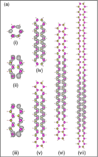
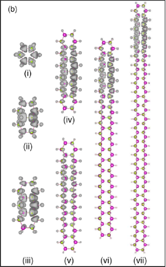
Table 1 gives the results of the calculations for passivated and
unpassivated CdSe nanorods of different lengths. BE per atom for passivated
structures indicates the same trend as that of non-passivated structures (See
inset of Fig. 1(b)), but is lower for passivated structures with low
aspect ratio. Thus, passivation takes care of the surface effects prevalent in
structures of lower aspect ratios. A comparison of local density of states
(LDOS) of these structures also indicates that passivation does not change the
intrinsic behavior of highest occupied molecular orbitals (HOMO) and lowest
unoccupied molecular orbitals (LUMO). Hence, we could safely conclude that
surface passivation is essential in case of such CdSe one dimensional
structures. Inspection of BG values of passivated nanorods shows a significant
increase by upto 1.1 eV for the smallest length of nanorod. Thus, surface
passivation removes the localized surface states from the gap region and these
results contradict “self-healing” reported by Puzder et al Puzder et al. (2004) in
their study of CdSe clusters in the form of wurtzite cages of different
diameters. In their work , Puzder et al observe that the surface relaxation in
CdSe nanostructures act in similar manner to that of passivated nanostructures
of CdSe by opening the gap substantially.
Figures 2(a) and (b) show the partial charge density plots for HOMO
and LUMO of passivated CdSe nanorods respectively. The partial charge density
distribution of HOMO is predominantly localized on Se atoms which comes from
the orbitals (which lie along the length of the rod) of the atoms while
that of LUMO is on both Cd and Se atoms arising from orbitals of both Cd
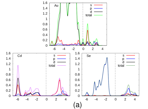
and Se throughout the nanorod. This is also reflected in the site projected DOS
(See Figure 3). For short nanorods, (<15 Å),
orbitals of Se atoms at the edges also contribute to HOMO. The range of partial
charge density arising from HOMO saturates at 39 Å for longer rods. In case
of LUMO, as the length of the nanorods increases, the contribution to the
partial charge density from Cd atoms, goes on decreasing. The span of LUMO
saturates over the length of 30 Å. The passivating agents show the
contribution from orbitals in the LUMO of the nanorods. Bader charge
analysis shows that the bonding between Cd and Se atoms in the nanorods has a
partial ionic character with Cd transferring an average charge of 0.55 on
Se.
III.2 Gold tipped CdSe nanorods
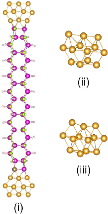
Global minimum geometry of Au13 cluster is found to be suitable to attach
at the ends of the nanorods. In this cluster, gold atoms are arranged in three
distinct planes. The bare clusters are attached to the fully relaxed nanorods.
These compound structures are then optimized fully forming a dumbbell-like
structure (nanodumbbell). We observe that the nanorods are unaffected due the
end passivation by gold electrodes, except at the M-S nanojunctions, where CdSe
bond length elongates to increase the area of the quadrilateral formed by two
CdSe pairs. Geometry of gold cluster however changes significantly (See Figures
4(ii) and (iii)). We can observe a slight buckling in three planes of
the cluster towards M-S interface. Both Cd and Se atoms at the ends of the
nanorods are doubly bonded to the Au atoms at the junctions, where Au-Cd and
Au-Se average bond lengths are 2.74 Å and 2.85 Å respectively.
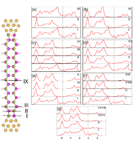
LDOS calculated for every plane of the gold tipped nanorods (See Figure
5), shows a gap near nanodumbbell center and metal induced gap states
(MIGS) emerge near M-S nanocontact. These MIGS vanish rapidly towards the
center of the nanorod Steiner et al. (2005); Landman et al. (2000). For short nanorods (upto
27 Å) bridging gold electrodes, we find full metallization by these
MIGS (Fig. 5(a), (b), (c) and (d)), while for longer nanorods, we
find a gap-structure emerging away from M-S junction. For longer nanorods, in
interfacial regions closest to the metal electrodes, a finite LDOS is observed
in the gap indicating a metallic nature which gradually decays away from the
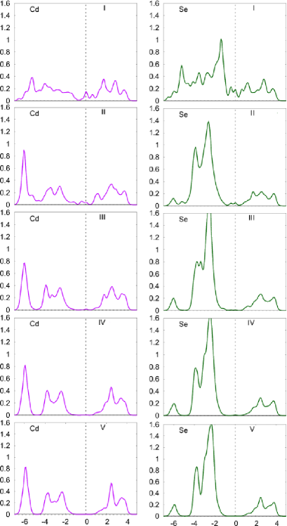
electrode. A comparison of site projected DOS for gold attached nanorods (See
Figure 3) and their separated components, shows the hybridization of
metal states with semiconductor states. There is maximum opening of the gap at
the central plane of nanodumbbell and the gap size decreases with increasing
length of the nanorod, eventually saturating to a value 2.05 eV. Figure
6 shows that the plane-wise site projected LDOS for
Au13Cd38Se38Au13 nanodumbbell where MIGS start vanishing rapidly across the
planes and central plane of the rod shows the presence of only semiconductor
states. MIGS are present only upto a distance of 15.5 Å from the
interface, thus making it clear why the nanorods shorter than 27 Å show full
metallization.
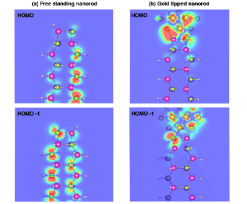
Figure 7 depicts the partial charge density plots for HOMO
and HOMO-1 states for free standing and gold attached passivated
Cd38Se38 nanorod. For the nanodumbbells, the HOMO and HOMO-1 states
are comprised of gold and states hybridized with states of Se and
states of Cd as shown in Fig. 7(b). This behaviour is also
evident from the LDOS plots in Fig. 6. Hybridization of gold
states with Cd states is not evident in the partial charge density plots.
However, gold induced states appear around Cd atoms in the contact plane (See
Fig. 6 - Plane I and II). The states of Se atoms comprising
the HOMO and nearby levels in free standing passivated Cd38Se38
nanorod have shifted below Fermi level () by 2 eV, while states near
HOMO in gold tipped nanorod mainly arise from gold and are spatially localized
near the contact plane. Bader charge analysis for the nanodumbbells shows that
changes in the charge transfer in comparison to free standing rods are
localized near the interface. Bonding remains same away from the interface. At
the interface, Cd atoms transfer an average charge of 0.68 while Se atoms
acquire an average charge of 0.53. The remaining charge gets distributed on
the gold cluster.
| Structures | Length | Schottky barrier | Gap at |
|---|---|---|---|
| height | central plane | ||
| (Å) | (eV) | (eV) | |
| Cd38Se38 | 39.43 | 1.00 | 2.12 |
| Cd74Se74 | 77.78 | 0.92 | 2.06 |
| Cd110Se110 | 116.66 | 0.93 | 2.05 |
Difference in work function of metal (Au) and electron affinity of
semiconductor (CdSe) yields a Schottky barrier when the two are brought in
contact. A decrease in the number of available states in confined structures
causes an increase in the energy barrier that carriers have to surmount in
order to cross the interface. Quantum confinement of carriers is known to
increase the minimum energy that a carrier has to have (relative to HOMO for
electrons and LUMO for holes) to propagate.
For an n-type semiconductor like CdSe, the Schottky barrier height (SBH) is
given by the difference between the metal work function and the electron
affinity of the semiconductor. This is calculated from the position of in
the nanodumbbell and the position of LUMO in the middle section of the CdSe
nanorod following Landman et al Landman et al. (2000). The values for SBH are listed in
Table 2. Group II-VI semiconductors have a higher component of
ionic bonding and hence these materials do not create large number of surface
states. Their barrier heights therefore depend upon the work function of the
metal. Here, the SBH for longer nanorods, which do not show metallization,
saturate for the nanorods having lengths longer than 78 Å.
IV Conclusions
In summary, we report that passivation of CdSe nanorods opens up the band gap
considerably and we do not observe any “self-healing” as reported by Puzder
et al Puzder et al. (2004) for their 3D structures. For free standing nanorods contribution
to HOMO comes mainly from orbitals of Se similar to bulk and 3D confined
structures. However contribution to LUMO comes from orbitals of Cd and Se
while for bulk and 3D structures LUMO mainly consists of Cd states. HOMO is
confined over a region of 39 Å, while LUMO is confined over 30 Å. Gold
attached nanorods are fully metalized for shorter lengths (< 27 Å),
while they develop a Schottky barrier, larger than the bulk value (0.7 eV at
300 KSze and Ng (2007)), for longer nanorods, where a semiconducting band gap starts to show
up at a distance of 15.5 Å from the nanojunction. End-passivated nanorods
and their separated components show charge transfer which is highly localized
at contact region.
All the figures of the structures are generated using VESTA Momma and Izumi (2008). We thank Department of Science & Technology, Government of India for financial support and C-DAC, Pune for use of their computing facilities.
References
- Steiner et al. (2005) D. Steiner, T. Mokari, U. Banin, and O. Millo, Phys. Rev. Lett. 95, 056805 (2005).
- Chan and Nie (1998) W. C. Chan and S. Nie, Science 281, 2096 (1998).
- Colvin et al. (1994) V. L. Colvin, M. C. Schlamp, and A. P. Alivisatos, Nature 370, 354 (1994).
- Klimov (2000) V. I. Klimov, Science 290, 314 (2000).
- Manna et al. (2000) L. Manna, E. C. Scher, and A. P. Alivisatos, J. Am. Chem. Soc. 122, 12700 (2000).
- Empedocles et al. (1999) S. A. Empedocles, R. Neuhauser, K. .Shimizu, and M. G. Bawendi, Adv. Mater. 11, 1243 (1999).
- Hu et al. (2001) J. Hu, L. Li, W. Yang, L. Manna, L. Ang, and A. P. Alivisatos, Science 292, 2060 (2001).
- Peng (2003) X. Peng, Adv. Mater. 15, 459 (2003).
- Barnard et al. (2006) A. S. Barnard, X. Huifang, L. Xiaochun, N. Pradhan, and X. Peng, Nanotechnology 17, 5707 (2006).
- de Paiva and Felice (2008) R. de Paiva and R. D. Felice, Am. Chem. Soc. NANO 2, 2225 (2008).
- Mokari et al. (2005) T. Mokari, C. G. Sztrum, A. Salant, E. Rabani, and U. Banin, Nature Materials 4, 855 (2005).
- Salant et al. (2006) A. Salant, E. Amitay-Sadovsky, and U. Banin, J. Am. Chem. Soc. 128, 10006 (2006).
- Costi et al. (2008) R. Costi, A. E. Saunders, E. Elmalem, A. Salant, and U. Banin, Nano Letters 8, 637 (2008).
- Landman et al. (2000) U. Landman, R. N. Barnett, A. G. Scherbakov, and P. Avouris, Phys. Rev. Lett. 85, 1958 (2000).
- Demechenko and Wang (2007) D. O. Demechenko and L. W. Wang, Nano Lett. 7, 3219 (2007).
- Meulenberg et al. (2009) R. W. Meulenberg, J. R. I. Lee, A. Wolcott, J. Z. Zhang, L. J. Terminello, and T. Buuren, ACS Nano 3, 325 (2009).
- Kresse and Furthmuller (1996) G. Kresse and J. Furthmuller, Phys. Rev. B 54, 11169 (1996).
- Blochl (1994) P. E. Blochl, Phys. Rev. B 50, 17953 (1994).
- Perdew et al. (1996) J. P. Perdew, K. Burke, and M. Ernzerhof, Phys. Rev. Lett. 77, 3865 (1996).
- Tang et al. (2009) W. Tang, E. Sanville, and G. Henkelman, J. Phys.: Condens. Matter 21, 084204 (2009).
- Sanville et al. (2007) E. Sanville, S. D. Kenny, R. Smith, and G. Henkelman, J. Comp. Chem. 28, 899 (2007).
- Henkelman et al. (2006) G. Henkelman, A. Arnaldsson, and H. Jonsson, Comput. Mater. Sci. 36, 254 (2006).
- Alivisatos (1996) A. P. Alivisatos, Science 271, 933 (1996).
- Heath (1999) J. M. Heath, Acc. Chem. Res. 32, 38 (1999).
- Yang et al. (2008) P. Yang, S. Tretiak, A. E. Masunov, and S. Ivanov, J. Chem. Phys. 129, 074709 (2008).
- Wang and Zunger (1996) L. W. Wang and A. Zunger, Phys. Rev. B 53, 9579 (1996).
- Shiraishi (1990) K. Shiraishi, J. Phys. Soc. Jpn. 59, 3455 (1990).
- Wang and Li (2004) J. W. Wang and J. Li, Phys. Rev. B 69, 153302 (2004).
- Huang et al. (2005) X. Huang, E. Lindgren, and J. R. Chelikowsky, Phys. Rev. B 71, 165328 (2005).
- Troullier and Martins (1991) N. Troullier and J. L. Martins, Phys. Rev. B 43, 1993 (1991).
- Puzder et al. (2004) A. Puzder, A. J. Williamson, F. Gygi, and G. Galli, Phys. Rev. Lett. 92, 217401 (2004).
- Sze and Ng (2007) S. M. Sze and K. K. Ng, Physics of Semiconductor Devices (John Wiley and Sons, Inc., New Jersey, 2007) page 179.
- Momma and Izumi (2008) K. Momma and F. Izumi, J. Appl. Crystallogr. 41, 653 (2008).