Hysteretic melting transition of a soliton lattice in a commensurate charge modulation
Abstract
We report on the observation of the hysteretic transition of a commensurate charge modulation in IrTe2 from transport and scanning tunneling microscopy (STM) studies. Below the transition ( K on cooling) a charge modulation was observed, which is consistent with previous studies. Additional modulations [] appear below a second transition at K on cooling. The coexistence of various modulations persist up to on warming. The atomic structures of charge modulations and the temperature dependent STM studies suggest that 1/5 modulation is a periodic soliton lattice which partially melts below on cooling. Our results provide compelling evidence that the ground state of IrTe2 is a commensurate 1/6 charge modulation, which originates from periodic dimerization of Te atoms visualized by atomically resolved STM images.
pacs:
71.45.Lr, 74.70.Xa, 74.70.-bA periodic electronic charge modulation, often called charge-density wave (CDW), is an ordering phenomenon which is accompanied by a distortion of the underlying lattice with the same periodicity Grüner (1988). The driving force of a CDW can be a Fermi surface nesting instability (also called Peierls transition; often considered the canonical mechanism of charge or spin density waves in low dimensional electronic systems Grüner (1988)), the indirect Jahn-Teller effect Jahn and Teller (1937), or the formation of local bound states Jérome et al. (1967); van Wezel and Littlewood (2010). Often the CDW periodicity is incommensurate with respect to the underlying lattice. The competition between these two periodicities may lead to a transition from an incommensurate phase to a specific commensurate phase, i.e. a lock-in transition below the CDW phase transition Bhatt and McMillan (1975); McMillan (1976); Chen et al. (1981, 1982).
An elegant picture of the lock-in transition is a melting transition of a soliton lattice with no soliton in the commensurate phase but a finite density of periodic solitons in the incommensurate phase Bhatt and McMillan (1975); McMillan (1976). While the commensurate phase is energetically favored at low temperature because of lower elastic energy cost and positive soliton energy, the incommensurate phase is favored by the driving mechanism (e.g. the nesting condition) and the entropy gain due to the formation of the soliton lattice McMillan (1976); Bak and von Boehm (1980). The continuous reduction of the soliton density results in a continuous variation of the incommensurability of the charge modulation, which is closely related to the famous devil’s staircase, where infinite commensurate phases with modulations at all possible fractional numbers emerge from competing microscopic interactions Bak and von Boehm (1980); Villain and Gordon (1980); Bak and Bruinsma (1982); Selke (1988).
Recently, an intriguing charge/orbital density wave was discovered in the 5d transition metal dichalcogenide IrTe2 with large spin-orbital coupling Yang et al. (2012); Pyon et al. (2012). Interestingly, superconductivity emerges with the suppression of the CDW phase Yang et al. (2012); Pyon et al. (2012); Fang et al. (2013), indicating that the coexistence of CDW and superconductivity in quasi-2-dimensional (Q2D) transition metal dichalcogenides is a general phenomenon. Originally, Fermi surface nesting has been suggested as the mechanism of the charge modulation in IrTe2 Yang et al. (2012). However, various experimental observations indicate that the local bonding states of Te orbitals and the mixed valence nature of Ir ions are more likely responsible for the driving force of the charge modulation Fang et al. (2013); Oh et al. (2013); Ootsuki et al. (2012). Therefore, it is imperative to visualize the local electronic modulation with atomic resolution to reveal the fundamental mechanism of charge modulation in IrTe2.
Herein, we report on the observation of an intriguing hysteretic transition ( K) of the commensurate charge modulation phase in IrTe2 below the previously reported transition ( K) using transport and STM measurements. The atomically resolved modulations suggest that the previously observed 1/5 modulation is a periodic lattice of solitonlike phase slips, similar to the unidirectional CDW due to periodic phase slips observed in strained NbSe2 Soumyanarayanan et al. (2013). In this picture, the hysteretic transition may be described as an incomplete melting of a soliton lattice with a sudden decrease of soliton density, resulting in short-range charge modulations described by . On warming the partially melted soliton lattice persists all the way to . The partial melting transition and the coexistence of multiple fractional modulations are similar to the characteristics of the devil’s staircase phenomena Bak and von Boehm (1980); Villain and Gordon (1980). Our high-resolution STM data suggest that the intrinsic ground state of IrTe2 is likely an 1/6 modulation with periodic Te dimer stripes.
Single crystalline IrTe2 specimens were grown from the Te flux. STM experiments were performed in an ultra-high vacuum (UHV) multifunctional chamber with a base pressure mbar. The single crystals were cleaved in UHV at room temperature (RT) to expose the pristine (001) surface, presumably terminated by the Te layer. STM images were acquired in constant-current mode with typical STM parameters of V and nA. Magnetization and electrical resistivity were measured up to 400 K using the Quantum Design MPMS-XL7 and PPMS-9. STM images were analyzed with WSXM Horcas et al. (2007).
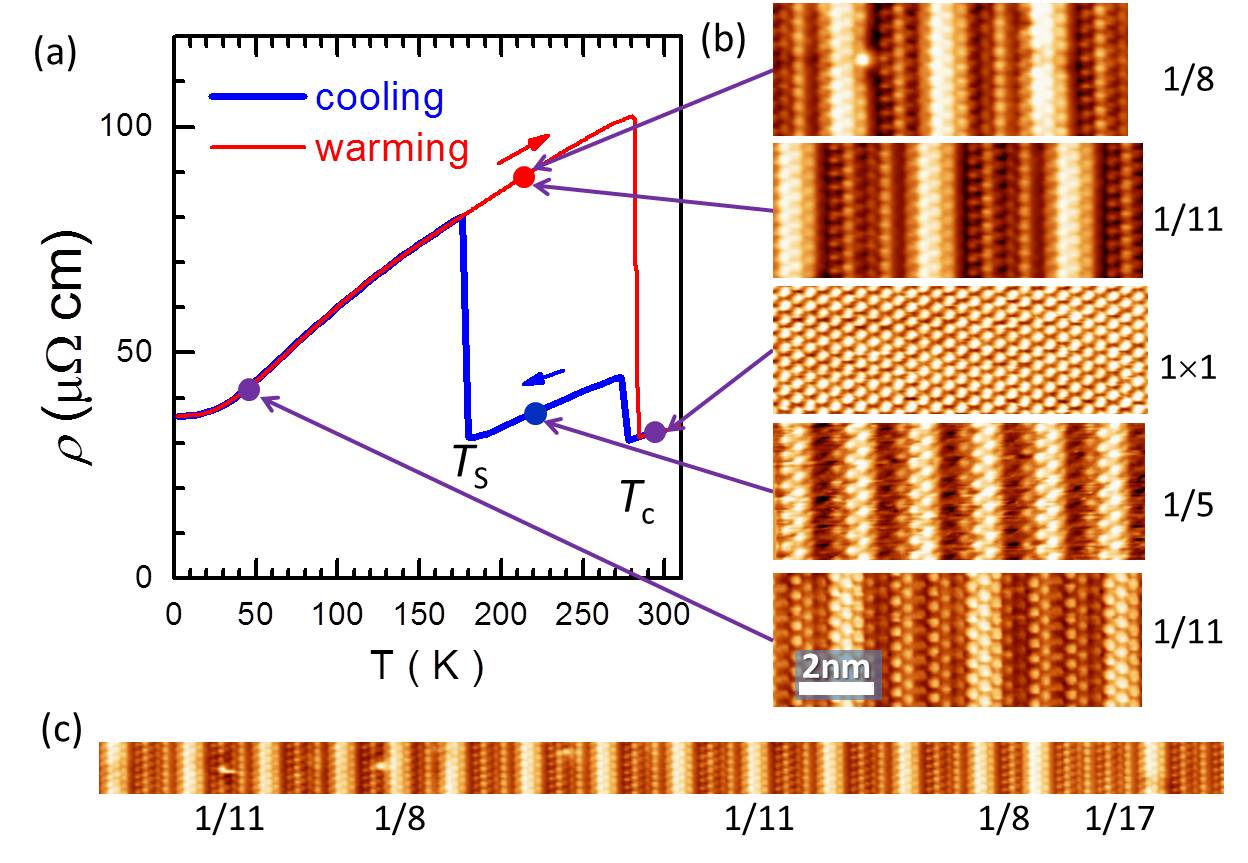
Figure 1(a) shows the typical data measured on a high quality single crystalline IrTe2 sample. In addition to the CDW transition () reported in earlier works Yang et al. (2012); Pyon et al. (2012); Fang et al. (2013); Oh et al. (2013), another transition can be recognized on cooling the sample at K which is also characterized by a resistivity increase. On warming, the high-resistivity state persists to without returning to the intermediate state. This unusually large hysteresis was reproduced in multiple single crystals, indicative of the significant metastability of the low temperature state. The absence of the second transition () in earlier works suggests that it is very sensitive to the sample quality. In fact, tiny inhomogeneous strain is sufficient to smear out the sharp anomalies 111See supplemental material..
Previous scattering studies suggest the CDW transition () is characterized by formation of a superstructure Yang et al. (2012); Oh et al. (2013). This is directly confirmed by our STM observation of 1/5(1,0) on the (001) surface at intermediate temperature (220 K) on cooling, while the RT-STM image in Fig. 1(b) shows the expected 11 atomic structure. Therefore, our STM observation of 1/5 modulation unlikely originates from surface reconstruction. Note (1)
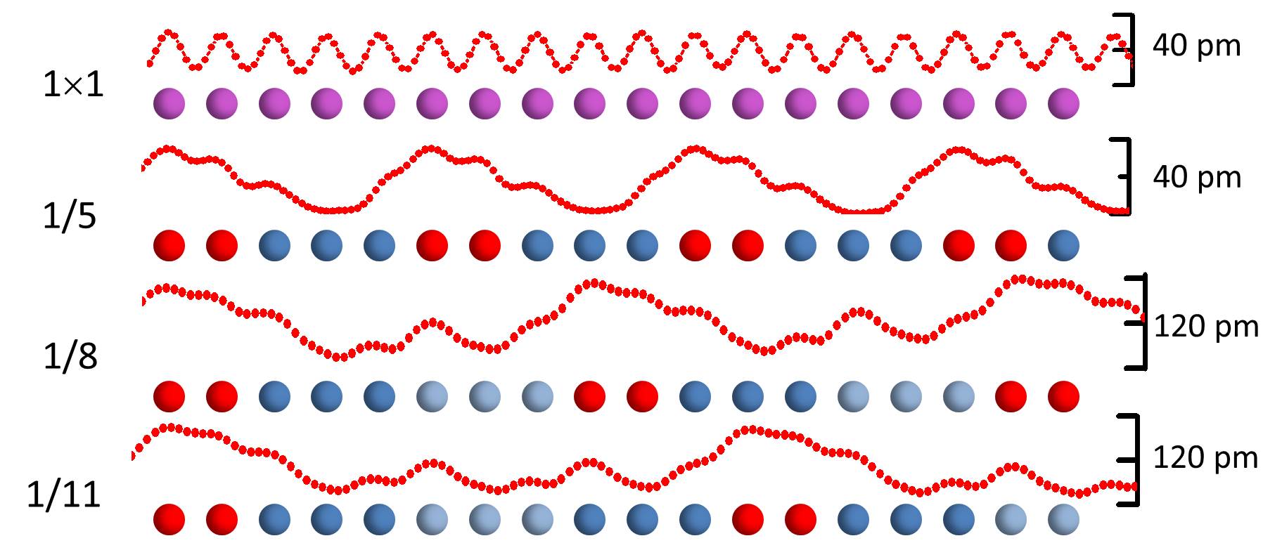
At new periodicities (e.g. 1/8, 1/11, etc.) with domain sizes of a few nanometers appear. They consist of double-columns (appearing bright in color-coded STM images) which are separated by an integer number of three-row blocks, as shown in Fig. 1. The two types of fundamental units, 2 and 3 atomic columns, are clearly visible in column-averaged line profiles which have been extracted from the atomically resolved STM images in Fig.1 and are plotted as red traces in Fig. 2. Here Å is the inter-column spacing, and is lattice constant. The composition for 2 and 3 units is highlighted by red and blue spheres, respectively. Thereby, our STM results suggest that the new modulations can be unified in a simple empirical relationship, namely, with . This picture suggests that the ground state of IrTe2 is probably a periodic structure of 3 columns. In this sense, a 2 column corresponds to a fractional phase slip, i.e. a soliton-like (anti-phase) boundary of the ground state Zhang et al. (2011); Soumyanarayanan et al. (2013). Within this picture the 1/5 modulation is a soliton lattice with maximal density, and the hysteretic transition is a partial “melting” of the soliton lattice. This scenario is very similar to the soliton lattice melting picture of the lock-in transition in Q2D CDW systems McMillan (1976); Chen et al. (1981, 1982).
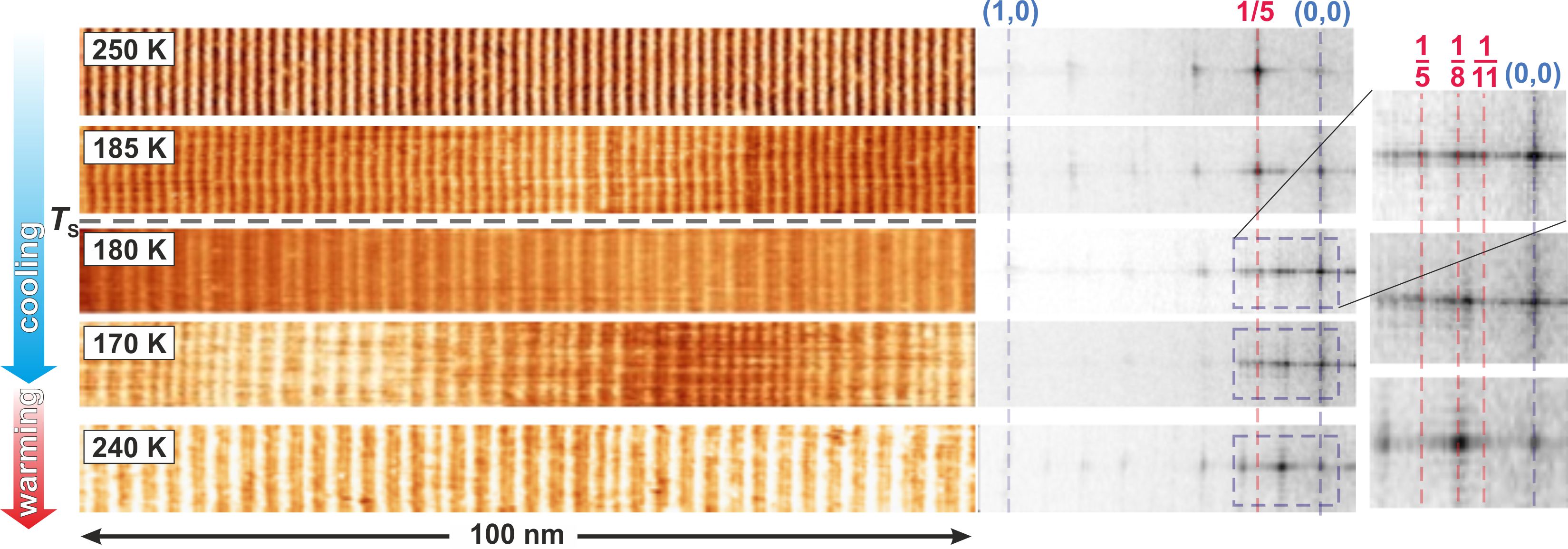
To reveal the mechanism of the second transition, we performed variable temperature STM studies of IrTe2 single crystals between 250 K and 140 K. Because of the lack of unique topographic features Note (1) it is difficult to keep track of the same surface area by compensating the thermal drift after each temperature change (unlike in previous studies Hsu et al. (2013)). To circumvent this difficulty, large-scale STM images with atomic resolution are needed for statistical analysis of the evolution of modulations. For this purpose, multiple () STM images with a width of 200 nm along the modulation direction were taken at various temperatures. Representative sections of STM images at 250, 185, 180, 170 (cooling) and 240 K (warming) and their corresponding fast Fourier transformed (FFT) images are shown in Fig. 3. Clearly a uniform 1/5 modulation is observed in the intermediate temperature range with correlation length over many microns, resulting in sharp 1/5 spots in FFT maps. Similar to recent scattering studies, the second harmonic peak (2/5) is quite strong, suggesting a non-sinusoidal modulation Pascut and Kiryukhin (2013); Cao et al. (2013). Interestingly, new modulations of longer wavelengths but very short correlation lengths appear below as shown in STM images, which is consistent with the diffusive superlattice streaks Note (1). The short correlation lengths suggest that the new modulations probably nucleate and get trapped inside the original 1/5 domains. Consistently, negligible change of soliton density across was observed near a twin domain boundary with two different directions (not shown here), excluding the twin boundaries as possible nucleation centers of new modulations. On warming the correlation length of 1/8 increases substantially resulting in a sharp spot in FFT map (at 240 K), indicative of thermal annealing of the soliton lattice.
Figure 4 summarizes our counting statistics of STM observation Note (1). Fig. 4(a) shows the -dependence of normalized soliton density (bright 2 columns in STM topographic images, such as in Fig. 3) where is the soliton density from data and is that of pure 1/5 modulation. Above , the soliton density is almost 100%, while it drops significantly to across , which is in good agreement with transport data Note (1). As decreases further, continues to decrease, indicating that solitons are energetically unfavorable in the low temperature phase. On warming stays at up to 240 K, in good agreement with the transport data in Fig. 1(a). The anti-correlation between and suggests that the solitons (2) has a lower resistivity than the ground state (3). In contrast to the significant increase of soliton lattice correlation length (of 1/8) on warming, the has a similar slope as that of the intermediate phase (1/5), indicating that the defect scattering of conduction electrons is not sensitive to the disorders of the soliton lattice. Therefore, the sharp increase of resistivity at is mainly caused by a reduction of density of states at Fermi level (), indicating that solitons have a higher than the ground state. Consistently, the solitons appear higher in constant-current STM topography at low bias.
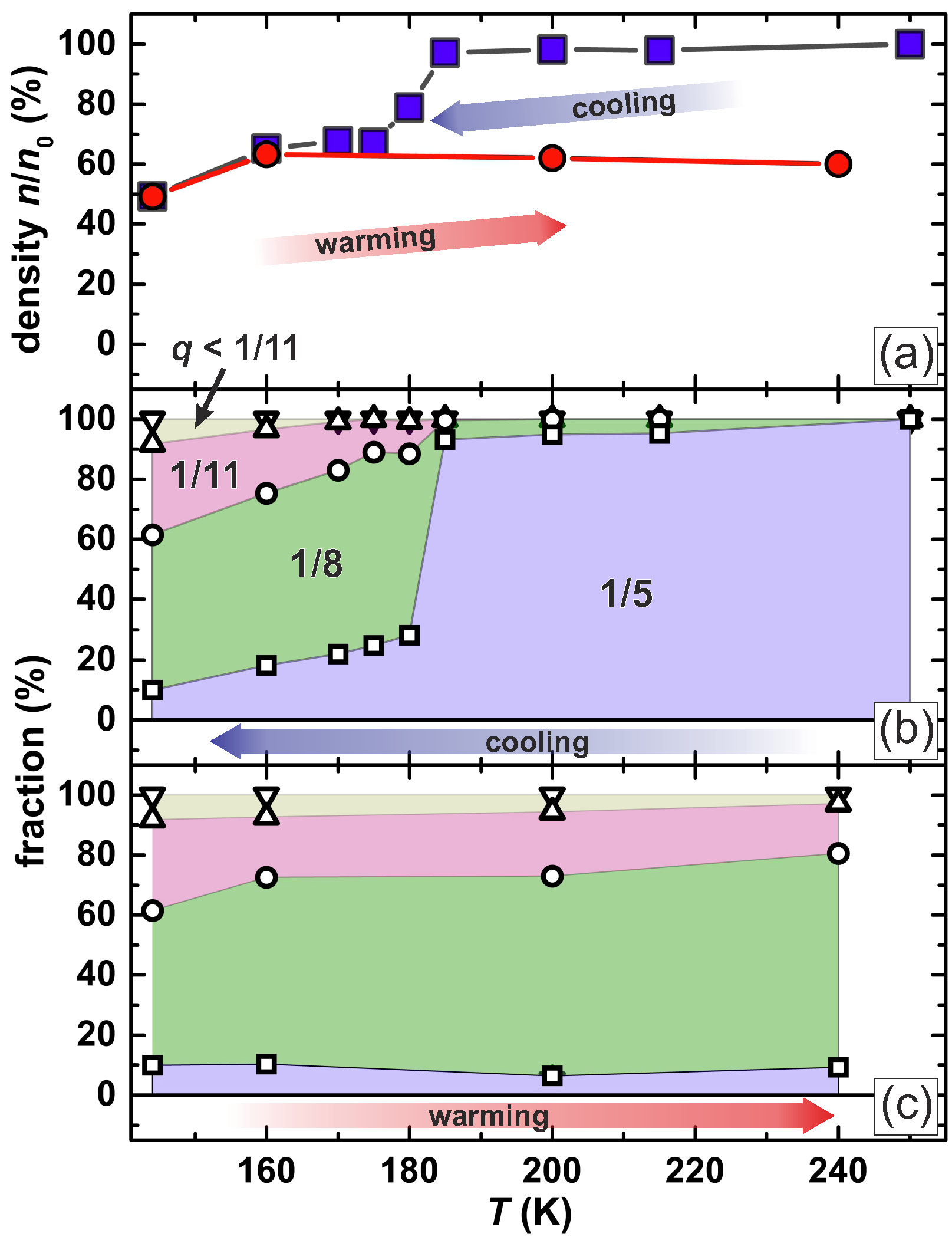
More detailed information can be obtained from the areal fractions of individual modulations (1/5, 1/8, 1/11, etc.) shown in Fig. 4(b) and (c). The areal fractions of various modulations show similar hysteretic behaviors, i.e., significant changes across on cooling but minor changes on warming. Specifically, the fraction of 1/5 reduces drastically from over 90% to across , while the fractions of other modulations (especially 1/8) increase substantially.
All of our STM data are consistent with the soliton lattice picture of commensurate charge modulations discussed in above text, which provides a simple unified description [] of all the observed modulations in IrTe2. The soliton lattice melting transition at indicates that the ground state of IrTe2 consists of a periodic structure of stripes. Indeed, a abrupt change of modulation from 1/5 to 1/6 was observed in Se doped IrTe2 where the transition temperature systematically increases with increasing Se concentration Oh et al. (2013). Because Se is more electronegative than Te, this observation provides compelling evidence that the CDW transition is likely caused by breaking Te-Te bonds Oh et al. (2013). However, the origin of the 1/6 modulation is unclear in previous studies Oh et al. (2013). Our STM results provide a natural explanation of the 1/5 to 1/6 transition in Se doped IrTe2, namely, that the weakening of Te-Te bonds by Se doping energetically favors the intrinsic ground state of 1/6 super-structure (i.e. a doubling of stripes). This scenario is supported by the observation of a sudden increase of the thermal hysteresis () of at the boundary between 1/5 and 1/6 Oh et al. (2013).
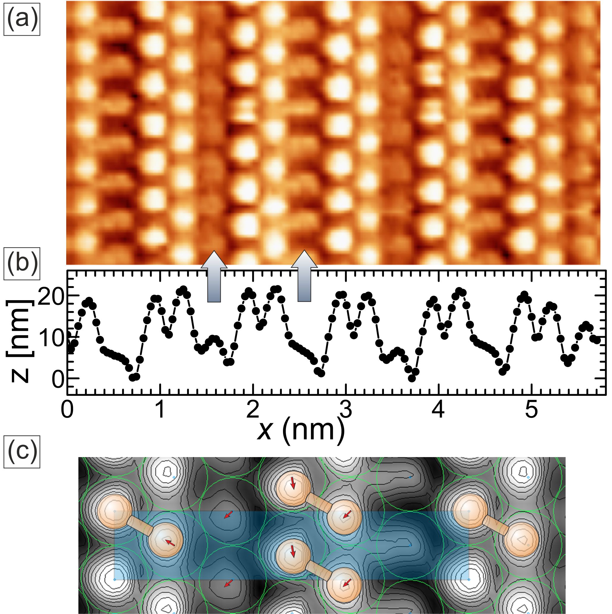
Our picture is further corroborated by the occasional observation of large patches (dimension over 100 nm) of purely 1/6 modulation (i.e. no soliton) below in IrTe2. A zoom-in STM image with atomic resolution of the 1/6 modulation and its corresponding line profile are shown in Fig. 5(a) and (b). There is a subtle difference between the neighboring stripes, as indicated by the two arrows in Fig. 5. The microscopic origin of the two kind of stripes is unclear at this moment. The spacing between two bright atomic rows (3.0 Å) is significantly smaller than the mean inter-column spacing (3.4 Å), indicating a formation of Te double-rows separated by unpaired Te rows. Detailed analysis of atomic displacements of Te atoms within the supercell [shown in Fig. 5(c)] indicates the formation of Te dimers within each Te double-row. The atomic displacements with respect to the undistorted lattice are approximately (unit: Å): , and , which are derived from column averaged profiles ( displacements) and inter-column cross-correlations ( displacements). The Te dimer stripes might be induced by the formation of Ir4+ dimers proposed by high resolution x-ray scattering analysis Pascut and Kiryukhin (2013).
Previous studies suggested that the charge modulation transition originates from breaking of the Te-Te bonds because of mixed valence states of Ir (3+/4+) Jobic et al. (1992); Ootsuki et al. (2012); Fang et al. (2013); Oh et al. (2013). Since there exists one hole in the orbital of an Ir4+ ion Radaelli et al. (2002), it has been speculated that the charge modulation is associated with orbital rearrangement Pyon et al. (2012), which is supported by XPS measurements and scattering refinements Ootsuki et al. (2012); Cao et al. (2013). Single crystal x-ray scattering refinement analyses suggest that both Ir and Te form periodic dimer stripes below Pascut and Kiryukhin (2013), which is consistent with our STM observation.
In conclusion, we have carried our a systematic high resolution STM study of the charge modulated phases in high quality single crystals of IrTe2 and discovered a hysteretic melting transition of soliton lattice that occurs only on cooling. Our results suggest that the previously reported 1/5 modulation is a periodic soliton lattice that partially melts at K. Our STM observation provides compelling evidence that the ground state of IrTe2 is an super-structure with periodic Te dimer stripes. The melting transition is interrupted probably by kinetic energy barriers due to the formation of a dilute soliton lattice with short-range modulations described by .
We thank G.L. Pascut and V. Kiryukhin for sharing unpublished x-ray results and the idea of dimerization. The work at Rutgers was supported by the NSF-DMREF-1233349 and DMR-0844807. The work at Postech was supported by the Max Planck POSTECH/KOREA Research Initiative Program [No. 2011-0031558] through the NRF of Korea funded by the Ministry of Education, Science and Technology. The work at Würzburg was supported by Deutsche Forschungsgemeinschaft within FOR 1162 (grant BO1468/20-1) and by the Alexander von Humboldt Foundation (WW).
References
- Grüner (1988) G. Grüner, Rev. Mod. Phys. 60, 1129 (1988).
- Jahn and Teller (1937) H. A. Jahn and E. Teller, Proc. R. Soc. London A 161, 220 (1937).
- Jérome et al. (1967) D. Jérome, T. M. Rice, and W. Kohn, Phys. Rev. 158, 462 (1967).
- van Wezel and Littlewood (2010) J. van Wezel and P. B. Littlewood, Physics 3, 87 (2010).
- Bhatt and McMillan (1975) R. N. Bhatt and W. L. McMillan, Phys. Rev. B 12, 2042 (1975).
- McMillan (1976) W. L. McMillan, Phys. Rev. B 14, 1496 (1976).
- Chen et al. (1981) C. H. Chen, J. M. Gibson, and R. M. Fleming, Phys. Rev. Lett. 47, 723 (1981).
- Chen et al. (1982) C. H. Chen, J. M. Gibson, and R. M. Fleming, Phys. Rev. B 26, 184 (1982).
- Bak and von Boehm (1980) P. Bak and J. von Boehm, Phys. Rev. B 21, 5297 (1980).
- Villain and Gordon (1980) J. Villain and M. B. Gordon, J. Phys. C: Solid State Phys. 13, 3117 (1980).
- Bak and Bruinsma (1982) P. Bak and R. Bruinsma, Phys. Rev. Lett. 49, 249 (1982).
- Selke (1988) W. Selke, Physics Reports 170, 213 (1988).
- Yang et al. (2012) J. J. Yang, Y. J. Choi, Y. S. Oh, A. Hogan, Y. Horibe, K. Kim, B. I. Min, and S.-W. Cheong, Phys. Rev. Lett. 108, 116402 (2012).
- Pyon et al. (2012) S. Pyon, K. Kudo, and M. Nohara, J. Phys. Soc. Jap. 81, 053701 (2012).
- Fang et al. (2013) A. F. Fang, G. Xu, T. Dong, P. Zheng, and N. L. Wang, Sci. Rep. 3, 1153 (2013).
- Oh et al. (2013) Y. S. Oh, J. J. Yang, Y. Horibe, and S.-W. Cheong, Phys. Rev. Lett. 110, 127209 (2013).
- Ootsuki et al. (2012) D. Ootsuki, Y. Wakisaka, S. Pyon, K. Kudo, M. Nohara, M. Arita, H. Anzai, H. Namatame, M. Taniguchi, N. L. Saini, and T. Mizokawa, Phys. Rev. B 86, 014519 (2012).
- Soumyanarayanan et al. (2013) A. Soumyanarayanan, M. M. Yee, Y. He, J. van Wezel, D. J. Rahn, K. Rossnagel, E. W. Hudson, M. R. Norman, and J. E. Hoffman, PNAS 110, 1623 (2013).
- Horcas et al. (2007) I. Horcas, R. Fernandez, J. M. Gomez-Rodriguez, J. Colchero, J. Gomez-Herrero, and A. M. Baro, Rev. Sci. Instrum. 78, 013705 (2007).
- Note (1) See supplemental material.
- Zhang et al. (2011) H. Zhang, J.-H. Choi, Y. Xu, X. Wang, X. Zhai, B. Wang, C. Zeng, J.-H. Cho, Z. Zhang, and J. G. Hou, Phys. Rev. Lett. 106, 026801 (2011).
- Hsu et al. (2013) P.-J. Hsu, T. Mauerer, W. Wu, and M. Bode, Phys. Rev. B 87, 115437 (2013).
- Pascut and Kiryukhin (2013) G. L. Pascut and V. Kiryukhin, private communication (2013).
- Cao et al. (2013) H. Cao, B. C. Chakoumakos, X. Chen, J. Yan, M. A. McGuire, H. Yang, R. Custelcean, H. Zhou, D. J. Singh, and D. Mandrus, (2013), arXiv:1302.5369 .
- Jobic et al. (1992) S. Jobic, R. Brec, and J. Rouxel, J. Solid State Chem. 96, 169 (1992).
- Radaelli et al. (2002) P. G. Radaelli, Y. Horibe, M. J. Gutmann, H. Ishibashi, C. H. Chen, R. M. Ibberson, Y. Koyama, Y.-S. Hor, V. Kiryukhin, and S.-W. Cheong, Nature 416, 155 (2002).