Fabrication and Characterization of Aluminum Airbridges for Superconducting Microwave Circuits
Abstract
Superconducting microwave circuits based on coplanar waveguides (CPW) are susceptible to parasitic slotline modes which can lead to loss and decoherence. We motivate the use of superconducting airbridges as a reliable method for preventing the propagation of these modes. We describe the fabrication of these airbridges on superconducting resonators, which we use to measure the loss due to placing airbridges over CPW lines. We find that the additional loss at single photon levels is small, and decreases at higher drive powers.
Superconducting coplanar waveguide (CPW) transmission lines and resonators are integral components of cryogenic detectors for submillimeter electromagnetic radiation, Mazin et al. (2012); Day et al. (2003) quantum memory elements, Hofheinz et al. (2009) and solid state quantum computing architectures. Galiautdinov et al. (2012); Mariantoni et al. (2011); Barends et al. (2013) The desired mode profile of a CPW is symmetric,Simons (2004) with the two ground planes on either side of the center trace held to the same voltage. However, asymmetries and discontinuities in the microwave circuitry can lead to the excitation of parasitic slotline modes.Ponchak et al. (2005) These modes can couple to elements of the circuit such as qubits, and they represent a source of radiation loss and decoherence.Harokopus and Katehi (1991); Houck et al. (2008)
In order to suppress these spurious modes, crossover connections need to be made between the ground planes that are interrupted by the CPW structure. Free standing crossovers, known as airbridges, have been a staple of conventional microwave CPW technology, Koster et al. (1989); Kwon et al. (2001) and fabrication processes have recently been developed for building airbridges on superconducting microwave circuits. Lankwarden et al. (2012); Abuwasib et al. (2013) However, the fabrication of airbridges adds additional processing that may degrade the quality of the circuit, and the airbridges themselves may present a source of loss. In addition, care must be taken in order to avoid accidentally creating tunnel junctions with small critical currents at the interfaces of such structures. In this Letter, we present the first characterizations of the loss due to fabricating airbridge crossovers on superconducting microwave resonators. We find that the loss due to airbridge crossovers is small but not negligible, and should be taken into account when engineering crossovers for low loss circuit elements.
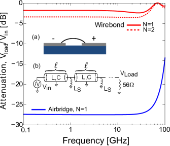
To motivate our use of airbirdges, we observe that in past work with superconducting circuits, connections between the different ground planes have been typically been made using wirebonds. However, with a wire diameter of 1 mil and a typical length of 1 mm, wirebonds have an inductance of order 1 nH Rosa (1908) and an impedance 40 at 6 GHz, making them an ineffective shunt. In comparison, airbridges have 100 times less inductance due to their small size. In order to understand the effect of the crossover impedance on slotline attenuation, we studied a simple transmission line model Wenner et al. (2011a) for the slotline with evenly spaced inductive shunts to ground as shown in Fig. 1(a). We simulated in SPICE 1 mm of a transmission line with with a terminated load, and varied the number of inductive shunts. As seen in Fig. 1, the attenuation per millimeter of the slotline propagation for a single airbridge is two orders of magnitude greater than for one or two wirebonds. This result can be easily understood if we consider only the inductances of the model, which is valid below the cutoff frequency.Wenner et al. (2011a) The inductance of 0.5 mm of the slotline is 0.23 nH, which is smaller than the wirebond inductance but much bigger than the inductance of an airbridge. Thus, in the case of wirebonds, signal will continue propagating down the line rather than flow to ground. Furthermore, while increasing the wirebond density can be difficult and unreliable, increasing the airbridge density can be done by simply redesigning a photomask. With 10 airbridges per mm, we simulated the attenuation to be -150 dB, implying the slotline mode does not exist.
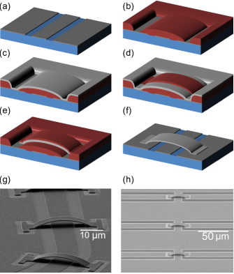
The fabrication process we used for the airbridges follows from earlier work done on kinetic inductance detectors,Lankwarden et al. (2012) with modifications to adapt the process for an aluminum base layer. We show the process flow and resulting structures in Fig. 2. First, we formed the scaffold for the bridge from a 3 m thick positive photoresist (Megaposit SPR-220-3). The thickness of the bridge is set by the resist thickness, and photolithography determines the placement and span of the bridge. Throughout the process we used a developer (AZ Dev 1:1) designed to minimize aluminum etching. Away from the bridge area, we did not expose the resist so that it remained as a protective layer and etch stop. Next, we reflowed the resist at 140∘C for 3 minutes to form an arch for mechanical stability. We then deposited 300 nm of aluminum in a high vacuum electron beam evaporator to form the bridge layer. Prior to the deposition, we used an in-situ argon ion mill calibrated to remove the native oxide of the base aluminum in order for the bridges to make good electrical contact.Barends et al. (2013) The ion mill was operated for 3.5 minutes in 1 mbar of argon, with beam voltage 400V, beam current 21 mA, and beam width 3.2". Using a second layer of patterend 3 m resist as a mask, we then wet etched (Transene Aluminum Etchant Type A at 30∘C) the excess deposited aluminum that is not used to form the bridge. We determined the termination of the etch by visual inspection. When the top layer of aluminum was etched away, the wafer went through a clear change in reflectance from aluminum to the underlying resist layer; the typical etch time was 5 minutes. We continued immersing the wafer in the etchant for 5 seconds after this transition, then immersed the wafer in water for 3 minutes. The termination of the etch is a critical step because the regions around the pads of the bridge are not protected by photoresist during the etch, and can potentially be etched through, breaking the ground plane. Finally, we stripped both layers of resist in an 80∘C heated bath of Microposit 1165 photoresist stripper to release the airbridges.
We initially confirmed that the argon ion mill step led to an ohmic contact at the bridge pads by measuring the room temperature resistance across multiple airbridges using a standard four terminal measurement. For ten airbridges in series that were 28 microns long and 8 microns wide, we found the resistance to be 6 , which is roughly consistent with the resistance of an aluminum wire of the same geometry. We further ruled out any thick oxide junctions by measuring the critical current across multiple airbridges below the critical temperature (1.2 K), which we found to be of order 100 mA.sup
In developing the process, we initially found a large amount of residual resist remained from the scaffolding layer after stripping in solvents. This decreased the reliability of our bridges by loading and deforming the bridge arches, and would have contributed a large amount of loss to our circuit. We deduced that the residue consisted of resist cross-linked by ion implantation from the argon ion mill step, a well known problem in semiconductor processing.Okuyama et al. (1978) We were able to mitigate the problem by stripping the resist layers in a downstream oxygen plasma at 150∘C for 5 minutes prior to stripping in a solvent bath. The low temperature oxygen plasma acts to burn off the damaged layer of resist.
With this additional cleaning step, we have been able to reliably fabricate bridges over a range of spans from 2 m to 50 m. The main sources of bridge failure are factors other than their structural stability such as lithographic errors, and the failure rate is less than 0.1%. We have also tested the bridges in a variety of postprocessing steps, including wafer dicing and fabricating aluminum junctions with a bilayer electron beam resist process; bridges spanning up to 40 m have been found to survive these steps reliably. We note here that the airbridges generally do not survive sonication.
To measure the loss added by placing an airbridge over a CPW transmission line, we constructed quarter wavelength CPW resonators with variable numbers of airbridges connecting the ground planes. We fabricated the resonators from an aluminum film deposited on a high-resistivity silicon subtrate and etched with a BCl3/Cl2 inductively coupled plasma.Megrant et al. (2012) We have also used the process on a sapphire substrate with comparable results. We designed the resonators with 10 m center traces and 5 m gaps to match the dimensions of our typical feedlines, and designed the resonant frequencies to range from 5 to 6 GHz. We designed the airbridges to have 4 m of clearance from the CPW line for a total length of 28 m, and chose an airbridge width of 8 m to ensure mechanical stability of the bridge. On eight of the resonators, we fabricated between 12 and 110 airbridges spanning the resonator center trace, evenly spaced in the number of bridges. The resonators with the most airbridges had a density of one airbridge every 50 m, covering 16% of the total length of the resonator. The remaining two witness resonators went through the full process of airbridge fabrication but were not designed with any airbridges spanning their center traces. We used these witness resonators as a test of whether placing airbridges on a CPW line adds loss to other circuit elements on the same wafer. We also fabricated a separate chip of resonators from the same film that saw no additional processing, to act as a control sample.
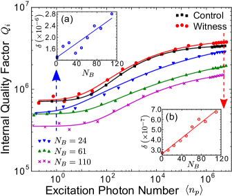
In order to determine the internal quality factor of the resonators, we placed them in an adiabatic demagnetization refrigerator (ADR), which reached a base temperature of 50 mK. We determined by measuring the transmission through a feedline that was capacitively coupled to each resonator (see Ref. Megrant et al., 2012 for measurement details). We varied the drive power such that the photon population in the resonator ranged from single photon levels up to photons, at which point the resonators became non-linear. A sample of representative quality factor data for some of the resonators is shown in the main panel of Fig. 3. As seen in previous work, the quality factor of the resonators increases as a function of increasing drive power, which is consistent with the loss in the resonator being dominated by two-level states (TLS) at the material interfaces.Megrant et al. (2012); Gao et al. (2008); Martinis et al. (2005); Sage et al. (2011)
In general, we expect the dependence of the quality factor to show two plateaus, one around single photon levels corresponding to loss being dominated by TLS, and one at high power corresponding to saturation of TLS.Megrant et al. (2012); Sage et al. (2011) From our control chip, for which a representative example is shown in black squares in Fig. 3, we determined that the nominal internal quality factor for our resonator geometry and material was around at single photon powers and at high power (5 million photons). Our witness resonators, for which a representative example is shown in red circles in Fig. 3, performed similarly, indicating that the additional processing on the chip did not add any loss. As we increased the number of bridges fabricated over the resonator, the quality factor decreased at both low and high powers. Interestingly, the quality factor does not appear to plateau as strongly at high power when airbridges are present.
To determine quantitatively the loss due to airbridges, we extracted the loss tangent at powers around a single photon and at 5 million photons. In Fig. 3a (3b), we plot the low power (high power) loss tangent as a function of number of airbridges, along with lines of best fit. From the slopes, we estimate that each airbridge adds to the loss tangent of the resonator at low power and at high power. We can also estimate the loss per fraction of the resonator that is covered by the resonator. If we assume that the loss also scales with the width of the airbridges, then every one percent of the resonator covered by airbridges adds an additional to the loss tangent at low power and at high power. We note that a resonator completely covered by airbridges would be limited to an internal quality factor of order 120,000 at low power, which is more than five times lower than the uncovered device.
To understand this increase in the loss due to airbridges, we note that the change in the loss at different drive powers suggests that the addition of an airbridge adds to the TLS loss of the resonator. However, the source of this additional TLS loss is unclear. Optical and SEM images show that despite our efforts to clean off the resist, residues still remain on some edges close to the pads of the bridge, some of which is visible in the lower left and top right contact pads shown in Fig. 2(g). The interface underneath the bridge is also suspect, since it was deposited on photoresist that had been crosslinked by the argon ion mill. However, the participation ratios of these regions are small since they are not in the regions of high field.Wenner et al. (2011b) As an example, through a simulation in COMSOL, we find that adding 100 nm of dielectric material with a loss tangent of (typical for amorphous oxides) and dielectric constant of 4 gives a loss tangent of , or a of 630,000 for complete airbridge coverage (see supplement for details). This is significantly higher than our measured value despite the fact that 100 nm is the upper bound on the interface thickness under the bridge based on SEM images.sup
In addition to placing airbridges over CPW lines to connect the ground planes together, we have also fabricated airbridges to connect two CPW center traces together. We tested such a connection by fabricating quarter wavelength CPW resonators with intentional breaks in the resonator, then reconnecting the lines with airbridges, as shown in Fig. 2(h). The resonators fabricated using this method performed comparably to resonators fabricated with ground plane airbridges, with each airbridge connection added to the center trace adding a loss of . More information about these measurements can be found in the supplement. These results indicate that airbridges can used be to carry microwave signals, and for example, allowing for the crossing of two perpendicular superconducting CPW lines.sup
In summary, we have fabricated reliable aluminum airbridges on an aluminum microwave circuit. Simple considerations of the inductances of a wirebond versus an airbridge show that airbridges are far superior for the purpose of attenuating slotline modes. However, placing them on CPW lines adds some additional loss proportional to the amount of airbridge coverage, which should be taken into consideration when building sensitive, low-loss microwave elements.
The authors thank J. Baselmans for helpful discussions and for providing test samples. Devices were fabricated at the UCSB Nanofabrication Facility, a part of the NSF-funded National Nanotechnology Infrastructure Network, and at the NanoStructures Cleanroom Facility. This research was funded by the Office of the Director of National Intelligence (ODNI), Intelligence Advanced Research Projects Activity (IARPA), through Army Research Office Grant No. W911NF-09-1-0375. All statements of fact, opinion, or conclusions contained herein are those of the authors and should not be construed as representing the official views or policies of IARPA, the ODNI, or the U.S. Government.
References
- Mazin et al. (2012) B. A. Mazin, B. Bumble, S. R. Meeker, K. O’Brien, S. McHugh, and E. Langman, Opt. Express 20, 1503 (2012).
- Day et al. (2003) P. K. Day, H. G. LeDuc, B. A. Mazin, A. Vayonakis, and J. Zmuidzinas, Nature 425, 817 (2003).
- Hofheinz et al. (2009) M. Hofheinz, H. Wang, M. Ansmann, R. C. Bialczak, E. Lucero, M. Neeley, A. O’Connell, D. Sank, J. Wenner, J. M. Martinis, et al., Nature 459, 546 (2009).
- Galiautdinov et al. (2012) A. Galiautdinov, A. N. Korotkov, and J. M. Martinis, Phys. Rev. A 85, 042321 (2012).
- Mariantoni et al. (2011) M. Mariantoni, H. Wang, T. Yamamoto, M. Neeley, R. C. Bialczak, Y. Chen, M. Lenander, E. Lucero, A. O’Connell, D. Sank, et al., Science 334, 61 (2011).
- Barends et al. (2013) R. Barends, J. Kelly, A. Megrant, D. Sank, E. Jeffrey, Y. Chen, Y. Yin, B. Chiaro, J. Mutus, C. Neill, et al., Phys. Rev. Lett. 111, 080502 (2013).
- Simons (2004) R. N. Simons, Coplanar Waveguide Circuits, Components, and Systems, vol. 165 (Wiley, 2004).
- Ponchak et al. (2005) G. E. Ponchak, J. Papapolymerou, and M. M. Tentzeris, IEEE Trans. Microw. Theory Techn. 53, 713 (2005).
- Harokopus and Katehi (1991) W. Harokopus and P. Katehi, in Microwave Symposium Digest, 1991., IEEE MTT-S International (IEEE, 1991), pp. 743–746.
- Houck et al. (2008) A. Houck, J. Schreier, B. Johnson, J. Chow, J. Koch, J. Gambetta, D. Schuster, L. Frunzio, M. Devoret, S. Girvin, et al., Phys. Rev. Lett. 101, 080502 (2008).
- Koster et al. (1989) N. Koster, S. Koblowski, R. Bertenburg, S. Heinen, and I. Wolff, in Microwave Conference, 1989. 19th European (IEEE, 1989), pp. 666–671.
- Kwon et al. (2001) Y. Kwon, H.-T. Kim, J.-H. Park, and Y.-K. Kim, IEEE Microw. Wireless Compon. Lett. 11, 59 (2001).
- Lankwarden et al. (2012) Y. Lankwarden, A. Endo, J. Baselmans, and M. Bruijn, J. Low Temp. Phys. 167, 367 (2012).
- Abuwasib et al. (2013) M. Abuwasib, P. Krantz, and P. Delsing, J. Vac. Sci. Tech. B 31, 031601 (2013).
- Rosa (1908) E. Rosa, Bulletin of the Bureau of Standards 4 (1908).
- Wenner et al. (2011a) J. Wenner, M. Neeley, R. C. Bialczak, M. Lenander, E. Lucero, A. O’Connell, D. Sank, H. Wang, M. Weides, A. Cleland, et al., Supercond. Sci. Tech. 24, 065001 (2011a).
- (17) See supplementary material for data on critical currents, shifts in resonant frequencies, and data on airbridge connections between CPW lines, and a discussion of surface loss.
- Okuyama et al. (1978) Y. Okuyama, T. Hashimoto, and T. Koguchi, J. Electrochem. Soc. 125, 1293 (1978).
- Megrant et al. (2012) A. Megrant, C. Neill, R. Barends, B. Chiaro, Y. Chen, L. Feigl, J. Kelly, E. Lucero, M. Mariantoni, P. OMalley, et al., Appl. Phys. Lett. 100, 113510 (2012).
- Gao et al. (2008) J. Gao, M. Daal, A. Vayonakis, S. Kumar, J. Zmuidzinas, B. Sadoulet, B. A. Mazin, P. K. Day, and H. G. Leduc, Appl. Phys. Lett. 92, 152505 (2008).
- Martinis et al. (2005) J. M. Martinis, K. Cooper, R. McDermott, M. Steffen, M. Ansmann, K. Osborn, K. Cicak, S. Oh, D. Pappas, R. Simmonds, et al., Phys. Rev. Lett. 95, 210503 (2005).
- Sage et al. (2011) J. M. Sage, V. Bolkhovsky, W. D. Oliver, B. Turek, and P. B. Welander, J. Appl. Phys. 109, 063915 (2011).
- Wenner et al. (2011b) J. Wenner, R. Barends, R. Bialczak, Y. Chen, J. Kelly, E. Lucero, M. Mariantoni, A. Megrant, P. OMalley, D. Sank, et al., Appl. Phys. Lett. 99, 113513 (2011b).