Near-field thermal transistor
Abstract
Using a block of three separated solid elements, a thermal source and drain together with a gate made of an insulator-metal transition material exchanging near-field thermal radiation, we introduce a nanoscale analog of a field-effect transistor which is able to control the flow of heat exchanged by evanescent thermal photons between two bodies. By changing the gate temperature around its critical value, the heat flux exchanged between the hot body (source) and the cold body (drain) can be reversibly switched, amplified, and modulated by a tiny action on the gate. Such a device could find important applications in the domain of nanoscale thermal management and it opens up new perspectives concerning the development of contactless thermal circuits intended for information processing using the photon current rather than the electric current.
pacs:
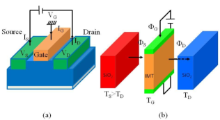
44.05.+e, 12.20.-m, 44.40.+a, 78.67.-nThe electronic solid-state transistor (Fig. 1) introduced by Bardeen and Brattain in 1948 Bardeen is undoubtedly the corner stone of almost all modern systems of information treatment. The classical field effect transistor (FET) which is composed by three basic elements, the drain, the source, and the gate, is basically used to control the flux of electrons (the current) exchanged in the channel between the drain and the source by changing the voltage applied on the gate. The physical diameter of this channel is fixed, but its effective electrical diameter can be varied by the application of a voltage on the gate. A small change in this voltage can cause a large variation in the current from the source to the drain. In 2006 Li et al. Casati1 have proposed a thermal counterpart of FET by replacing both the electric potentials and the electric currents by thermostats at a fixed temperature and heat fluxes carried by phonons through solid segments. Later, several prototypes of phononic thermal logic gates BaowenLi2 as well as thermal memories (see BaowenLiEtAl2012 and Refs. therein) have been developed in order to process information by phonon heat flux rather than by electric currents. However, this technology suffers from some weakness of fundamental nature which intrinsically limits its performance. One of the main limitations comes probably from the speed of acoustic phonons (heat carriers) which is four or five orders of magnitude smaller than the speed of photons. This explains, in part, why so many efforts have been deployed, during the last decades, to attempt to develop full optical or at least opto-electronic arcitectures for processing and managing information.

We introduce here a thermal transistor (Fig. 1) based on the heat transport by evanescent photons rather than by acoustic waves or electrons. This near-field thermal transistor (NFTT) basically consists of a gate made of an insulator-metal transition (IMT) material which is able to qualitatively and quantitatively change its optical properties through a small change of its temperature around a critical temperature . Vanadium dioxide (VO2) is one of such materials which undergoes a first-order transition (Mott transition Mott ) from a high-temperature metallic phase to a low-temperature insulating phase Baker close to room-temperature (). Different works have already shown van Zwol1 ; van Zwol2 ; vanZwol3 that the heat-flux exchanged at close separation distances (i.e. in the near-field regime) between an IMT material and another medium, can be modulated by several orders of magnitude across the phase transition of IMT materials. Further radiative thermal diodes have been recently conceived allowing for rectification Starr1936 ; RobertsWalker2011 of heat flux using materials with thermally dependend refractive indices OteyEtAl2010 ; Fan ; NefzaouiEtAl2013 and IMT materials PBA_APL . But so far controlling the heat flow with contactless systems to get the same functionalities as a classical FET has remained a challenging problem. Here we show that IMT materials are very promising candidates for designing efficient gates to control (switch, modulate or amplify) the heat flux exchanged between two media.
To start, let us consider the system as illustrated in Fig. 1(b), where two media which we call by analogy with a FET the source and the drain labeled by the indices and are maintained at temperatures and with by some thermostats. A thin layer of IMT material labeled by having a thickness is placed between both media at a distance from the source and the drain. Without external excitation, the system reaches its steady state for which the net flux received by the intermediate medium, the gate, is zero. In this case its temperature is set by the temperature of the surrounding media, i.e. the drain and the source. When a certain amount of heat is added to or removed from the gate (for example by applying a voltage difference through a couple of electrodes as illustrated in Fig. 1 or extracted from it using Peltier elements), its temperature can be either increased or reduced around its equilibrium temperature . Hence, the heat flux received by the drain and the flux lost by the source can be tailored accordingly. These heat fluxes correspond to the flux of Poynting vector across any plane separating the gate and the drain (and the source and the gate). In a three body system the flux received by photon tunneling by the drain reads Messina
| (1) |
where the monochromatic heat flux is given by
| (2) |
Here and denote the efficiencies of coupling of each mode between the source and the gate and between the gate and the drain for both polarization states ; is the wavevector parallel to the surfaces of the multilayer system. In the above relation denotes the difference of Bose-distributions functions and [with ] at the frequency ; is Boltzmann’s constant and is Planck’s constant. According to the N-body near-field heat transfer theory presented in Ref. Messina , the transmission coefficients and of the energy carried by each mode written in terms of optical reflection coefficients () and transmission coefficients of each basic element of the system and in terms of reflection coefficients of couples of elementary elements Messina
| (3) |
introducing the imaginary part of the wavevector normal to the surfaces in the multilayer structure ; is the velocity of light in vacuum. Similarly the heat flux lost by the source reads
| (4) |
where the transmission coefficients are analog to those defined in Eq. (3) and can be obtained making the substitution .
At steady state, the net heat flux received/emitted by the gate which is just given by the heat flux from the source to the gate minus the heat flux from the gate to the drain vanishes, i.e. or
| (5) |
This relation allows us to identify the gate equilibrium temperature (which is not necessary unique) for given temperatures and . Note that out of steady state the heat flux received/emitted by the gate is . If () an external flux is added to (removed from) the gate by heating (cooling).

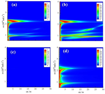
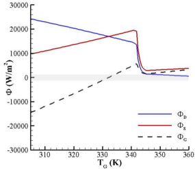
To illustrate the operating modes of NFTT we consider now a system composed by a source and a drain both made of silica (each coupled to a thermostat to maintain their local temperatures constant in time) and a gate made of vanadium dioxide VO2. When the gate temperature is smaller than its critical temperature , then the gate is in its monoclinic phase and it behaves as an uniaxial crystal. On the other hand, when the gate transits toward its amorphous metallic phase and remains in this state for greater temperatures. We consider here the case where the optical axis of VO2 film is orthogonal to its interfaces. The p-polarized transmission coefficients of the energy carried by the modes through such a system are plotted in Fig. 2. When the gate is in its crystalline state, , which represents the exchange between the source and the drain mediated by the presence of the gate [see Fig. 2(a)], and , which corresponds to the exchange between the couple source-gate treated as a unique body and the drain [see Fig. 2(b)] shows an efficient coupling of modes between the different blocks of the system around the resonance frequencies and of surface waves (surfaces phonon-polaritons) supported by both the source and the drain. Below all parts of the system support surface waves in the same frequency range close to the thermal peak frequency . The anti-crossing curves which appear in Fig. 2(a) and (b) result from the strong coupling of silica surface phonon-polaritons (SPPs) and the surface waves (symmetric and antisymmetric ones) suppported by the thin VO2 layer. Beyond the gate becomes amorphous (metallic) and it does not support surface wave anymore. In this case [see Fig. 2(c)] vansihes owing to the field screening by the gate. Moreover, as is clearly shown in Fig. 2(d), the coupling of modes between the couple source-gate and the drain at the frequency of surface waves is less efficient for the large parallel values of reducing so the transfer of heat towards the drain, i.e. the number of participating modes decreases BiehsEtAl2010 ; JoulainPBA2010 . By using different physical parameters (temperatures, sizes, separation distances…) several functions can be assigned to this system which can become either (i) a thermal switch, (ii) a thermal modulator or (iii) a thermal amplifier. We discuss below those operating modes. To do so we show Fig. 3 the net heat flux received by each part of the system in a particular configuration where , , and .
(i)Thermal switching :
In the situation depicted in Fig. (3) we have . An increase of by about 10 degrees ( is increased by ) leads, as clearly shown in Fig. 3, to a reduction of heat flux received by the drain and lost by the source by more than one order of magnitude. That means our NFTT can be used in two operating modes where is slightly below or above the critical temperature , where in the case we are in the ’on’ mode and for we are in the ’off’ mode.
(ii)Thermal modulation:
Over the temperature region around (gray shadow strip on Fig. 3) the heat current over the gate remains quite small (i.e. ) while the flux received by the drain or lost by the source can be modulated from high to low values. The thermal inertia of the gate as well as its phase transition delay of IMT material define the timescale at which the modulator can operate. A much larger modulation of fluxes can be achieved with the NFTT when using . Then the flux can be modulated over one order of magnitude by a small temperature change of .
(iii)Thermal amplification:
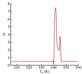
The most important feature of a transistor is its ability to amplify the current or electron flux towards the drain. In the region of phase transition around we see that an increase of leads to a drastic reduction of flux received by the drain. This corresponds to a negative differential thermal conductance as recently described for SiC in Ref. Fan (note that this behavior does not violate the second principle of thermodynamics because the heat flux continues to flow from the hot to the cold body). Having a negative differential thermal conductance is the key for having an amplification which is defined as (see for example Ref. Casati1 )
| (6) |
where
| (7) |
It can be easily shown that for much smaller or larger than where the material properties of VO2 are more or less independent of , since . On the other hand, inside the transition region of VO2 that means for temperatures around the material properties of VO2 change drastically showing a negative differential thermal resistance/conductance which leads to an amplification, i.e. . This behaviour is qualitatively demonstrated in Figs. 3 and 4 where the dielectric permittivity of VO2 in the transition region is modelled using a Bruggeman mixing rule as introduced in Ref. Mott . Hence, by chosing the temperatures such that the NFTT works as an amplifier.


The ability to control the flow of heat at subwavelength scale in complex architectures of solids out of contact, opens up new opportunities for an active thermal management for dissipating systems. It also suggests the possibility to develop contactless thermal analogs of electronic devices such as thermal logic gates and thermal memories, for processing information by utilizing thermal photons rather than electrons. Unlike other schemes for creating thermal transistors which were so far based on the control of acoustic phonons, the present concept authorizes much higher operational speeds (speed of light) and should be very competitive compared to the previous ones. We think also that the near-field thermal transistors could find broad applications in MEMS/NEMS technologies and could be used to generate mechanical works by modulating the heat flux received by the drain, by using microresonators such as cantilvers in contact with it.
References
- (1) J. Bardeen and W. H. Brattain, Phys. Rev. 74, 230 (1948).
- (2) B. Li, L. Wang and G. Casati, Appl. Phys. Lett. 88, 143501 (2006).
- (3) L. Wang, B. Li, Phys. Rev. Lett. 99, 177208 (2007).
- (4) N. Li, J. Ren, L. Wang G. Zhang, P. Hänggi and B. Li, Rev. Mod. Phys. 84, 1045 (2012).
- (5) M. M. Qazilbash, M. Brehm, B. G. Chae, P.-C. Ho, G. O. Andreev, B. J. Kim, S. J. Yun, A. V. Balatsky, M. B. Maple, F. Keilmann, H. T. Kim, D. N. Basov, Science, 318, 5857, 1750-1753 (2007).
- (6) A. S. Barker, H. W. Verleur, and H. J. Guggenheim, Phys. Rev. Lett. 17, 1286 (1966).
- (7) P. van Zwol, K. Joulain, P. Ben-Abdallah, J. J. Greffet and J. Chevrier, Phys. Rev. B (R), 83, 20, 201404 (2011).
- (8) P. van Zwol, K. Joulain, P. Ben-Abdallah and J. Chevrier, Phys. Rev. B(R), 84, 161413 (2011).
- (9) P. J. van Zwol, L. Ranno, and J. Chevrier, Phys. Rev. Lett. 108, 234301 (2012).
- (10) C. Starr, J. Appl. Phys. 7, 15 (1936).
- (11) N. A. Roberts and D. G. Walker, Int. J. thermal Sciences 50, 648 (2011).
- (12) C. R. Otey, W. T. Lau, and S. Fan, Phys. Rev. Lett. 104, 154301 (2010).
- (13) L. Zhu, C. R. Otey, and S. Fan, Appl. Phys. Lett. 100, 044104 (2012).
- (14) P. Ben-Abdallah and S.-A. Biehs, arXiv:1307.3154, (2013).
- (15) E. Nefzaoui, J. Drevillon, Y. Ezzahri, and K. Joulain, arxiv:1306.6209v1 (2013).
- (16) R. Messina, M. Antezza and P. Ben-Abdallah, Phys. Rev. Lett. 109, 244302 (2012).
- (17) Handbook of Optical Constants of Solids, edited by E. Palik (Academic Press, New York, 1998).
- (18) S.-A. Biehs, E. Rousseau, and J.-J. Greffet, Phys. Rev. Lett. 105, 234301 (2010).
- (19) P. Ben-Abdallah and K. Joulain, Phys. Rev. B 82, 121419(R) (2010).