Long Range Surface Plasmons in Multilayer Structures
Abstract
We present a new strategy, based on a Fresnel coefficient pole analysis, for designing an asymmetric multilayer structure that supports long range surface plasmons (LRSP). We find that the electric field intensity in the metal layer of a multilayer LRSP structure can be even slightly smaller than in the metal layer of the corresponding symmetric LRSP structure, minimizing absorption losses and resulting in LRSP propagation lengths up to . With a view towards biosensing applications, we also present semi-analytic expressions for a standard surface sensing parameter in arbitrary planar resonant structures, and in particular show that for an asymmetric structure consisting of a gold film deposited on a multilayer of SiO2 and TiO2 a surface sensing parameter can be achieved.
I Introduction
Surface plasmon polaritons (or “surface plasmons” (SP) for short) are excitations at metal-dielectric interfaces involving both electronic and electromagnetic degrees of freedom SP . They have attracted interest for a wide range of applications, including waveguiding and biosensing Barnes ; SP_sensing_rev ; berini_sensing , despite the fact that absorption in the metal typically restricts their propagation length to only a few tens of microns. These losses can be minimized if a thin metal layer is situated between two media – a cladding above and a substrate below – with the same dielectric constant. In this symmetric structure the SPs at the two metal-dielectric interfaces can couple and form an excitation in which most of the energy is in the bounding dielectrics, resulting in small propagation losses and propagation lengths of the order of a few millimeters. For this reason, these excitations are called long range surface plasmons (LRSP)LRSP ; stegeman . They can survive if the cladding and substrate dielectric constants are not identical, as long as the difference is not too great.
When the cladding above the metal film is a gas or liquid, as in biosensing applications, it is challenging to find a solid substrate that comes close to matching the cladding dielectric constant. If the cladding is an aqueous solution, Teflon and Cytop are two of the few candidate materials that can provide such a match cytop ; teflon . An alternate approach is to design an asymmetric layered structure that can support LRSP; examples include a suspended waveguide structure Berini1 and 1D photonic crystal structures Konopsky1 ; Konopsky2 . In this paper, we present a new approach to the design of asymmetric structures for LRSPs, based on a Fresnel coefficient pole analysis. Motivated by biosensing applications, we consider a water cladding, and focus on minimizing the electric field in the metal in order to reduce the losses. In a scenario where the structure is used for sensing the presence of a layer of molecules adsorbed onto the metal film from the water, we calculate the value of a standard surface sensing parameter berini_sensing ; Berini1 that results, and show that in the limit of thin molecular layers it can be derived from a semi-analytic expression that also follows from the pole analysis.
The organization of this paper is as follows: In Sec. II we present our approach for designing a periodic multilayer structure supporting LRSPs. In Sec. III we compare the field intensity profile of the LRSP supported by the multilayer structure to the LRSP in a symmetric structure, and calculate absorption and coupling losses for finite symmetric and asymmetric structures. In Sec. IV we derive a semi-analytic expression for a standard sensing parameter used to characterize the effect of thin molecular layers on the optical properties of arbitrary planar resonant structures, and compare exact and approximate calculations for the structures studied in Sec. III. The paper ends with our conclusions and a comparison with related work.
II Asymmetric multilayer structures for LRSPs
As a reference we begin by considering a symmetric structure, consisting of a thin layer of metal of thickness with a dielectric constant , sandwiched between a cladding and substrate of the same dielectric constant (Fig. 1a). The Fresnel reflection coefficient for light incident on the metal from the cladding, with wavevector component parallel to the interfaces, is
| (1) |
where and formalism1 . For real we define the square root according to , with if ; this guarantees that in the limit the reflected and transmitted fields, following respectively from Eq. (1) and the corresponding transmission coefficient, are either evanescent moving away from the structure, or carry energy away from it. The and are respectively the Fresnel reflection and transmission coefficients from medium , with dielectric constant , to medium , with dielectric constant . For -polarized light the coefficients are
| (2) | |||||
and for -polarized light they are
| (3) | |||||
where .
Surface electromagnetic resonances are generally signalled by poles in the Fresnel coefficients, indicating that fields can exist near the surface in the absence of incident light. Thus the condition for the LRSP excitation is
| (4) |
For -polarized light this can be satisfied at a resonance wavenumber , which is complex due to absorption in the metal. The real part of is greater than , indicating a field structure bound to the region of the thin film. We note that the extension of from the real axis to the complex plane can introduce subtleties associated with the definition of the square root in ; we will turn to those in Sec. III, but they will not affect the discussion in this section.
As an example of a symmetric structure we consider a gold metal layer with a thickness , with water as the cladding and substrate. At a wavelength of , and with dielectric constants of water and gold taken as Berini1 and Berini1 , a numerical search of in the complex plane identifies the LRSP by finding the complex value where (4) is satisfied for -polarized light; we find an effective index for the LRSP of , where . The very small imaginary part leads to a mode loss of about 2.23dB/mm (also considered by Min et al. Berini1 ), or equivalently an energy propagation length of about .
For any typical LRSP symmetric structure, such as the one above, we suppose that has been found. We now want to design an asymmetric structure (Fig. 1b), where the substrate has been replaced by a multilayer, to support LRSPs that mimic those of Fig. 1a.
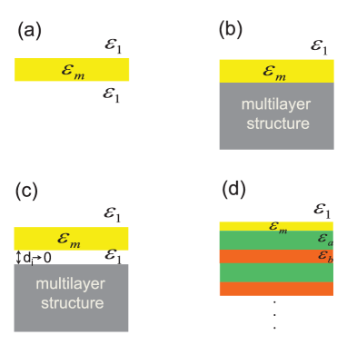
Any surface electromagnetic resonances in this new structure are signalled by poles in the Fresnel coefficients, for example in the reflection coefficient for light incident from the cladding, ,
| (5) |
where is the Fresnel reflection coefficient for light incident from a semi-infinite metal placed above the multilayer structure of interest in Fig. 1b. The reflection coefficient, , has a pole when
| (6) |
This will clearly lead to a equal to (recall Eq. (4)), if
| (7) |
where the Fresnel coefficients are evaluated at ; we take this as our design target. We can simplify it so that it only involves the properties of the metal layer through a dependence on by the following strategy: Insert an infinitesimally thin layer, with a thickness of and dielectric constant , between the metal layer and the multilayer (Fig. 1c). Then is easily found to be
| (8) |
where is the Fresnel reflection coefficient for light incident from the cladding to the multilayer structure, when there is no metal layer present. From Eq. (8), it is clear that (7) is satisfied if at .
We now specialize to a periodic multilayer structure consisting of layers and with respectively thicknesses and and real dielectric constants and . For an infinite periodic structure, the Fresnel coefficient is given by
| (9) | |||||
where we have assumed the top layer is of type , and is the reflection coefficient for light incident on the periodic structure from a semi-infinite medium of dielectric constant (see Fig. 1d). In the second line of Eq. (9), we have used the Fresnel coefficient identities and formalism2 , and from that line we find that the condition is satisfied if
| (10) |
which we refer to as our matching condition. When considering the propagation of the LRSP, if the multilayer is to simulate a uniform substrate with dielectric constant equal to that of the cladding, or at least nearly so, this condition must be satisfied, or nearly satisfied, when the Fresnel coefficients are evaluated at .
To establish a protocol for designing such a multilayer, it is useful to begin by neglecting all loss in the cladding and the metal, and any that might be present in the multilayer. In this approximation is replaced by its real part, and and are replaced by their real parts. This lossless approximation will allow us to winnow down the parameter space easily, to the point that the design can be completed; thus until the last three paragraphs of this section we assume and to be real in our analyses, and use the real parts of the actual quantities in our calculations.
Since we immediately have , indicating that the field is evanescent in the cladding, and thus from (10) we must have . If the dielectric constants of the layer materials are large enough so that the fields are propagating within the layers themselves ( and real), this requires that at we are within one of the photonic band gaps of the multilayer structure, so that the overall field structure is evanescent in the multilayer, and the reflectivity is of unit norm. To identify the condition for this to be so, note that the unit cell transfer matrix of the periodic multilayer structure is , with the interface transfer matrix between medium and , and the propagation transfer matrix in medium formalism2 ; is calculated from the eigenvector of ,
| (11) |
with eigenvalue , where , and is the complex Bloch wavenumber. For an overall field structure that is evanescent in the multilayer structure, signalling that we are in a photonic band gap, we must have yariv . Writing the unit cell matrix elements by , , , and ,
| (12) |
we have
| (13) |
with
| (14) |
yariv . The matrix elements of (12) are found by multiplying the transfer matrices of which it is composed; in particular we find
| (15) | |||||
Location within a band gap ( purely imaginary, real) is thus signalled by . At the band edges, and yariv . It is within the band gaps that we have , and it is there we must seek to satisfy Eq. (10).
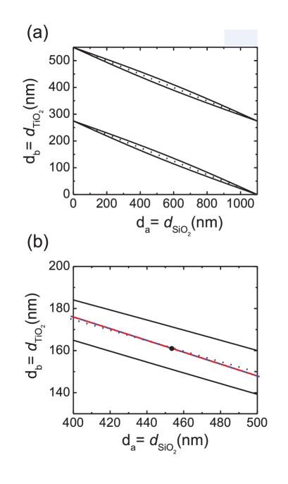
We consider addressing this task once a choice of multilayer materials has been made, with and fixed. If we then consider letting , any existing band gap will necessarily vanish, since the medium will become uniform, and at best we can have in the limit. From (15) we see that as there are only discrete where this will hold; only for these does the band gap survive until . We can plot these as points in the plane of points . Similarly, as there are only discrete for which , signalling for which the band gap will survive until . Connecting the corresponding discrete points and in the plane by straight lines should then give a rough indication of the location of the band gaps as and are varied. Those straight lines are easily found to be identified by
| (16) |
We illustrate this by considering periodic multilayers of SiO2 and , taking the dielectric constants of SiO2 and TiO2 as Berini1 and refractive_index , respectively. In Fig. 2a we plot the solutions of Eq. (16) as dotted lines. The solid lines indicate the solutions for the band edges ( for and in general both nonzero), with the region in between each pair of lines indicating the values of for which there is a photonic bandgap. We see that the dotted lines do indeed give a good indication of where in the plane the band gaps lie; we refer to the lines identified by Eq. (16) as guide lines. Note that the canonical “quarter-wave stack” with , lies within the first band gap and in fact is precisely on the line (16) with .
To satisfy the matching condition (10) at we must be in the band gap region () and have . It is easy to determine where the latter condition is satisfied in the band gap region, and we plot that as the blue dash dotted line in Fig. 2b, together with the solutions of Eq. (16), again as dotted lines, where we focus on a region of the plane where the guide line is close to the center of the band gap region. Thus in the lossless limit it is possible to choose a multilayer structure so that (10) is exactly satisfied, and the LRSPs in the symmetric and antisymmetric structures share the same . We note that while the structures that do this are characterized by values that lie close to the guide lines, the solutions of do not run all the way to and , as do the guide lines, for before those limits are reached the solutions encounter the band edges.
We now reinstate loss in and in the water cladding. We no longer have automatically holding in the previously identified band gap regions of the plane, as we did in the absence of loss, and so to achieve (10) we would have to satisfy two nontrivial conditions, and . We can find curves in the plane where each of these conditions is satisfied, but for our choice of materials these curves do not intersect. So at least for some choices of dielectric materials it is impossible to satisfy (10) at in the ubiquitous presence of loss; we cannot simply replace a uniform substrate with a periodic multilayer structure and maintain the same LRSP.
Nonetheless, we can find complex values of close to where (10) is satisfied. They can be identified by choosing thicknesses close to one of the guide lines, and searching in the complex plane for values of that satisfy (10); we denote such solutions by . In fact this is possible for a wide range of values , indicated by the red lines in Fig. 2b. The guide lines provide a good indication of where the values of interest should be sought, although as in the lossless limit solutions cannot be found all the way to and . Note that in general the different points on the red line in Fig. 2b correspond to different values of , unlike the different points on the blue dash dotted line, which all correspond to solutions of Eq. (10) with the Fresnel coefficients evaluated at .
A reasonable design strategy is to adopt thicknesses associated with the center of the band gap region, resulting in an LRSP with a field in the multilayer well-confined near the metal, and for which we can expect a better tolerance for any fabrication errors. In line with this, but still somewhat arbitrarily, we take and for the rest of this paper. This yields an , corresponding to a loss of 2.15dB/mm and an energy propagation length of about . The real part of is very close to the real part of , and the loss for the asymmetric structure is actually slightly less than for the LRSP of the original symmetric structure. Thus while our original goal was to match and achieve the low loss of a LRSP in a symmetric structure, we find that using a multilayer structure it is possible to achieve even lower loss than in a symmetric structure; we plan to return to this in future communications.
III Symmetric and asymmetric LRSP fields
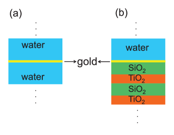
Some insight into the nature of the LRSPs in the infinite symmetric and asymmetric structures we have considered (see Fig. 3) can be gained by comparing the LRSP field profiles in the two structures. A fair comparison involves field profiles that are associated with the different structures and have the same field energy. Since loss is present, the field energy for a LRSP cannot be strictly defined, but since the loss is small in the sense that the LRSP can propagate many wavelengths before decaying, we can proceed by replacing the complex quantity , where is the position and frequency dependent dielectric constant, by Re, and using the standard expression for energy density in a dispersive medium to construct mode profiles corresponding to the same energy in both structures navin . Scaling the electric field intensity (i.e., ) of the field profiles of the two structures in the same way yields the results shown in Fig. 4.
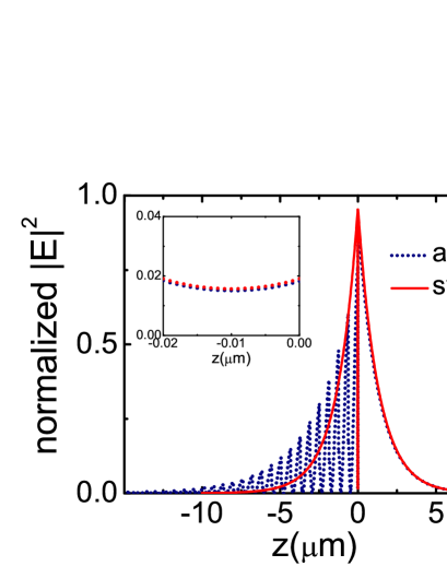
The electric field intensity in the cladding () is evanescent, and almost the same in the two structures. In the metal layer (inset), the electric field intensity in the multilayer structure is similar to, and even slightly smaller than, the field intensity in the symmetric structure; it is for this reason that the loss of the mode in the asymmetric structure is slightly smaller than that of the mode in the symmetric structure. While is symmetric about the center of the gold film in the symmetric structure, it exhibits an evanescent envelope function in the multilayer in the asymmetric structure. However, due to the multiple reflections and interferences in the layers, there are oscillations in indicative of the photonic band gap. Compared to an earlier proposed multilayer structure for the LRSP Konopsky2 , in this structure the field is less confined, but is also much smaller in the metal layer, and therefore the absorption losses are smaller.
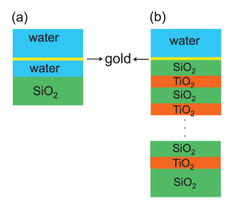
In realistic structures the behaviour of the fields is modified by the presence of substrates. While we continue to treat the cladding as infinite, assuming that in sensing applications the thickness of the water above the gold will be greater than the evanescent decay length of the field, we now consider the gold to be deposited on a finite multilayer structure with an SiO2 substrate (see Fig. 5b). For comparison we also consider a structure with an SiO2 substrate placed a finite distance below the gold film in an otherwise symmetric structure (see Fig. 5a). The properties of the LRSP that result in these structures can be studied by considering coupling into them with an incident field from the substrate, which is the usual Kretschmann configuration Kretschmann . In such an excitation the field inside the cladding is typically maximized when the rate of energy absorption in the metal layer equals the rate of energy incident from the substrate, and thus this usually identifies an optimum structure for sensing applications. Although this design target can be identified by pole analysis strategies unpublished , it can also be found simply by examining a series of reflectivity calculations for different thicknesses. For the symmetric structure we find that this critical coupling occurs when the thickness of the water layer below the gold film is about , and for the asymmetric structure we find that it occurs when the number of periods is , leading to a multilayer thickness of .
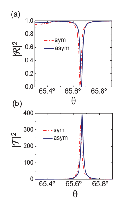
In Fig. 6a we plot the reflectivity of the two structures, each at its critical coupling thickness, as a function of incident angle; is the Fresnel coefficient for -polarized light incident from the substrate. The enhancement of the fields at the surface of each structure is determined by the Fresnel transmission coefficient from the substrate to the cladding for -polarized light, , and we see from Fig. 6b that enhancements in the square of the field of the order of is expected. The narrow resonances shown in these plots indicate poles in the Fresnel coefficients and . With respect to the poles in the corresponding infinite structures (see Fig. 3), the real parts of the poles are shifted slightly and the imaginary parts increased (and thus the loss increased) due to radiative coupling into the substrate. A search in the complex plane finds the pole for the symmetric structure at , where , with the imaginary part corresponding to a loss of about 4.6dB/mm, or equivalently an energy propagation length of about , and the pole for the asymmetric structure at , where , with the imaginary part corresponding to a loss of about 4.39dB/mm, or equivalently an energy propagation length of .
The dips in the reflectivities in Fig. 6a occur at angles associated with the real part of effective indices, and respectively, where is the index of refraction of the substrate at , and the widths of the dips are associated with the imaginary parts of the effective indices.
We note that the poles of the Fresnel coefficients extracted from equations such as Eq. (4) are used to approximate the values of Fresnel coefficients by pole expansions valid for real , which are the appropriate for excitation in a Kretschmann configuration as discussed here, or for use in superpositions to describe pulse propagation along a structure finite_beam . Thus in extracting these poles we should choose a definition of the square roots of such that the calculated values of the Fresnel coefficients in the upper half of the complex plane join continuously to those calculated on the real axis. Here this can be guaranteed by choosing a branch cut that lies along the negative imaginary axis.
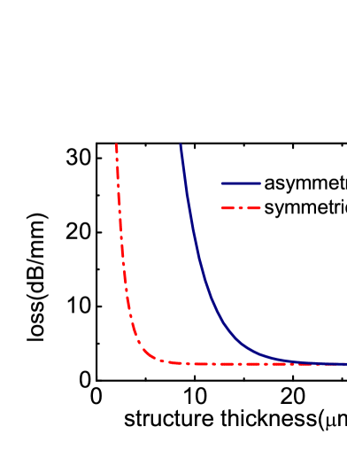
If we turn from Kretschmann configurations to applications involving end-fire coupling into LRSPs, optimization for sensing applications typically involves the minimization of propagation loss. That loss decreases as the thickness of the structure between the metal film and the substrate increases, for as increasing thickness the radiative loss of light into the substrate becomes less and less. In Fig. 7 the calculated losses of the LRSPs in the symmetric and asymmetric structures are shown as a function of the thickness of the structure, as extracted from the poles of the Fresnel coefficients. In the symmetric structure, for a water layer thickness larger than about the mode loss approaches a limiting value of 2.23dB/mm, corresponding to the mode loss of the infinite structure; in the asymmetric structure, for a multilayer thickness larger than about ( periods), the mode loss approaches a limiting value of 2.15dB/mm, corresponding to the mode loss of the infinite structure.
IV Sensing with Planar Resonant Structures
Resonant structures supporting guided modes, such as those considered above, have their optical properties modified by the presence of new species on or near the surface of the structure. This can lead to their application as sensors, for the new species are located precisely where the optical fields are largest, and thus their effect on the properties of the guided modes can be significant. In this section we derive a semi-analytic expression for a standard surface sensing parameter that characterizes the effectiveness of such a sensor, and apply it to the structures we have introduced in the last section.
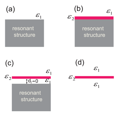
We begin generally and consider an arbitrary planar resonant structure (Fig. 8a), supporting a resonant mode at a complex wavenumber . If a thin molecular layer with effective dielectric constant is placed on the structure (Fig. 8b), the complex wavenumber of the mode shifts, and a surface sensing parameter can be defined berini_sensing as
| (17) |
where , and is the complex wavenumber of the mode in the presence of the molecular layer.
For close to we can use a pole expansion finite_beam ; aida_spont for the reflection coefficient from the cladding to the bare resonant structure, which we now denote very generally by , such that
| (18) |
where characterizes the pole strength and is in general complex. For the resonant structure with the molecular layer on top, modelled as a thin dielectric film, we can construct an expression for the Fresnel reflection coefficient in terms of by adding an infinitesimally thin layer, with a thickness and a dielectric constant , just below the molecular layer (Fig. 8c). Then
| (19) |
where and are the Fresnel reflection and transmission coefficients for the molecular layer sandwiched between two media with dielectric constant (Fig. 8 d). Inserting Eq. (18) in Eq. (19),
| (20) |
implying that the complex wavenumber of the mode in the presence of molecules, , is , and the shift in the complex wavenumber is
| (21) |
The pole strength is a parameter of the bare resonant structure, and does not depend on the properties of the molecular layer; in general it must be determined numerically. The reflection coefficient (see Fig. 8d), however, is
| (22) |
where is the thickness of the molecular layer, and , , , and are the Fresnel reflection and transmission coefficients between the cladding and the molecular layer (recall (2),(3)). Inserting Eq. (2) or (3) into Eq. (22), for thin molecular layers, where
| (23) |
for -polarization we find
| (24) |
with
while for -polarization
| (25) |
where
These calculations agree with the similar calculations presented earlier by Cheng et al. rangan ; using Eq. (24) or (25), and (21) in Eq. (17), we find a semi-analytic expression for the surface sensing parameter in terms of the thickness of the molecular layer, the dielectric constants of the molecular layer and the cladding, and the pole strength. We assume a molecular layer with an effective index of refraction of and thickness up to , and calculate the sensing parameters for the symmetric and asymmetric structures discussed in the previous section, both exactly by numerically determining the shift in the position of the pole of the full structures, and approximately from the semi-analytic expressions presented in this section; here the -polarized expressions are the relevant ones.
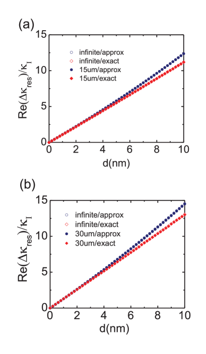
In Fig. 9 we show the results for of the infinite symmetric and asymmetric structures. The semi-analytic calculations match with the exact calculations for , but as the thickness of the molecular layer increases the assumption (23) loses its validity and the approximated calculations deviate more from the exact calculations; nonetheless, they remain accurate to about for thicknesses as large as . The slope of the curves in Fig. 9 around gives , and we find and for the infinite symmetric and asymmetric structure, respectively; the larger for the asymmetric structure is due to the slightly smaller resonance width () in the asymmetric structure. From Fig. 7, it is clear that if the thickness of the finite symmetric (or asymmetric) structure is larger than about (or ), the loss in the structure is about the loss in the corresponding infinite structure. As expected, the results for for a symmetric structure and a asymmetric structure are indistinguishable from the corresponding infinite structures, as shown in Fig. 9.
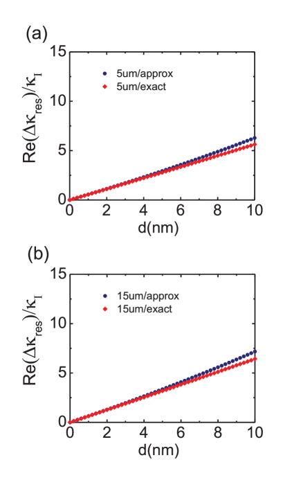
We have done similar calculations for the finite symmetric and asymmetric structures at thicknesses corresponding to the critical coupling thickness ( for the symmetric structure and for the asymmetric structure), and the result is shown in Fig. 10. These would be relevant for sensing in a Kretschmann configuration rather than an end-fire coupling configuration. We find and for the finite symmetric and asymmetric structures, respectively, which are smaller than the corresponding values shown in Fig. 10, as the coupling losses are larger here.
V Conclusion
In this paper we have presented a new strategy for designing asymmetric multilayer structures that support LRSPs. We have shown that if the Fresnel reflection coefficient from the cladding to the multilayer structure below the metal film vanishes at the complex wavenumber of the LRSP in a symmetric structure, the LRSP resonance condition for the symmetric and asymmetric multilayer structures become the same, and the asymmetric structure supports a LRSP equivalent to that supported in the symmetric structure. For an arbitrary choice of materials for the multilayer structure it is impossible to satisfy this condition exactly, but at complex wavenumbers close to that of the LRSP in the symmetric structure a resonance condition can be found, in some instances with even less loss than that of the LRSP in the symmetric structure.
We have provided a protocol for determining this resonance condition based on first describing a model system without loss, and then including the loss in the final design. We have also studied how the losses depend on the thickness of the multilayer structure, taking into account radiative contributions to the substrate. For a multilayer of SiO2 and TiO2 we have found that the radiative losses are negligible if the multilayer structure thickness is about or greater than . For biosensing applications involving an arbitrary planar resonant structure, we have derived a semi-analytic expression for a standard surface sensing parameter identifying the dependence of the sensing parameter on the dielectric constant of the molecular layer, its thickness, and the original pole strength of the resonance on the bare structure; for typical parameters we find that there is a good match between these semi-analytic expressions and the exact results if the thickness of the molecular layer is less than about , with corrections only on the order of about for molecular layer thicknesses up to . For a gold film the surface sensing parameter for the thick multilayer structure is , larger than the value of for a thick symmetric structure.
Compared to the gold structure of Min et al. Berini1 , which has an intensity attenuation of 3.26dB/mm and a surface sensing parameter , our asymmetric multilayer structure has a smaller loss (minimum of 2.15dB/mm) and a similar sensing parameter (). However, the structure of Min et al. Berini1 is a thin film suspended in air, and compared to our multilayer structure is expected to be less stable and harder to fabricate. Compared to the multilayer structure studied by Konopsky et al. Konopsky2 , the multilayer structure we present here is fully periodic, and does not require an additional layer between the metal and the periodic multilayer. However, a direct comparison of the losses and the surface sensing parameters of these two structures is not possible, as the metal layer in the work of Konopsky et al. Konopsky2 is palladium, which is lossier than gold. Nevertheless, if the number of the periods in that multilayer structure is increased from periods, the mode losses can be decreased by a factor of two. More generally, the design strategy presented here can be applied to a range of structures involving other metals and other multilayers to systematically explore the parameter space and optimize the predicted behavior.
In previous work aida_spont , we calculated Raman scattering from molecules on planar resonant dielectric structures, and showed that the Raman signal is enhanced when the pump field couples to a resonant mode. The asymmetric multilayer structure we studied in this paper can also be used as a substrate for surface enhanced Raman scattering (SERS) sers , when the pump field is coupled to the LRSP excitation. In particular, we expect that the good surface functionalization of gold films may make these structures more promising SERS substrates than fully dielectric multilayer structures srini .
VI Acknowledgements
This work was supported by BiopSys: the Natural Sciences and Engineering Research Council of Canada Strategic Network for Bioplasmonic Systems.
References
- (1) H. Raether, Surface Plasmons on Smooth and Rough Surfaces and on Gratings (Springer, 1988).
- (2) W. L. Barnes, A. Dereux, and T. W. Ebbesen, “Surface plasmon subwavelength optics,” Nature 424, 824-830 (2003).
- (3) J. Homola, S. S. Yee, and G. Gauglitz, “Surface plasmon resonance sensors: review,” Sens. Actuators B Chem. 54, 3-15 (1999).
- (4) P. Berini, “Bulk and surface sensitivities of surface plasmon waveguides,” New Journal of Physics 10, 105010(1)-105010(37) (2008).
- (5) D. Sarid, “Long-Range Surface-Plasma Waves on Very Thin Metal Films,” Phys. Rev. Lett. 47, 1927-1930 (1981).
- (6) J. J. Burke, G. I. Stegeman, and T. Tamir, “Surface-polariton-like waves guided by thin, lossy metal films,” Phys. Rev. B 33, 5186-5201 (1986).
- (7) A. W. Wark, H. J. Lee, and R. M. Corn, “Long-range surface plasmon resonance imaging for bioaffinity sensors,” Anal. Chem. 77 , 3904-3907 (2005).
- (8) R. Slavik, and J. Homola, “Ultrahigh resolution long range surface plasmon-based sensor,” Sens. Actuators B Chem. 123, 10-12 (2007).
- (9) Q. Min, C. Chen, P. Berini, R. Gordon, “Long range surface plasmons on asymmetric suspended thin film structures for biosensing applications,” Optics Express 18, 19009-19019 (2010).
- (10) V. N. Konopsky and E. V. Alieva, “Long-Range Propagation of Plasmon Polaritons in a Thin Metal Film on a One-Dimensional Photonic Crystal Surface,” Phys. Rev. Lett. 97, 253904(1)-253904(4) (2006).
- (11) V. N. Konopsky and E. V. Alieva, “Long-range plasmons in lossy metal films on photonic crystal surfaces,” Optics Express 34, 479-481 (2009).
- (12) For details of the notation used here for Fresnel coefficients, see formalism2 .
- (13) J. E. Sipe, “New Green function formalism for surface optics,” J. Opt. Soc. Am. B 4, 481-489 (1987).
- (14) A. Yariv and P. Yeh, Optical Waves in Crystals (Wiley, 2003).
- (15) http://refractiveindex.info/.
- (16) N. A. R. Bhat and J. E. Sipe, “Hamiltonian treatment of the electromagnetic field in dispersive and absorptive structured media,” Phys. Rev. A 73, 063808(1)-063808(25) (2006).
- (17) E. Kretschmann and H. Raether, “Radiative decay of nonradiative surface plasmons excited by light,” Z. Naturforsch. A 23, 2135-2136 (1968).
- (18) J.E. Sipe, unpublished.
- (19) J. E. Sipe and J. Becher, “Surface energy transfer enhanced by optical cavity excitation: a pole analysis,” J. Opt. Soc. Am. A 72, 288-295 (1982).
- (20) A. Delfan, M. Liscidini, and J. E. Sipe, “Surface enhanced Raman scattering in the presence of multilayer dielectric structures,” J. Opt. Soc. Am. B 29, 1863-1874 (2012).
- (21) T. Cheng, C. Rangan, and J. E. Sipe, “Metallic nanoparticles on waveguide structures: effects on waveguide mode properties and the promise of sensing applications,” J. Opt. Soc. Am. B 30, 743-765 (2013).
- (22) E. L. Ru and P. Etchegoin, Principles of Surface-Enhanced Raman Spectroscopy: and related plasmonic effects (Elsevier Science, 2008).
- (23) S. Pirotta, X.Xu, A. Delfan, S. Mysore, S. Maiti, G. Dacarro, M. Patrini, M.Galli, G. Guizzetti, D. Bajoni, J.E. Sipe, G. Walker, and M. Liscidini, “Surface enhanced Raman Scattering in purely dielectric structures via Bloch Surface Waves,” J. Phys. Chem. 117, 6821-6825 (2013).