Electronic transmission through AB-BA domain boundary in bilayer graphene
Abstract
We study the electron transmission through the domain boundary on bilayer graphene separating AB and BA stacking regions. Using the effective continuum model, we calculate the electron transmission probability as a function of the electron energy and the incident angle, for several specific boundary structures. The transmission strongly depends on the crystallographic direction of the boundary and also on the atomic configuration inside. At the low energy, the boundary is either insulating or highly transparent depending on the structure. In insulating cases, the transmission sharply rises when the Fermi energy is increased to a certain level, suggesting that the electric current through the boundary can be controlled by the field effect. The boundary parallel to the zigzag direction generally have different transmission properties between the two different valleys, and this enables to generate the valley polarized current in a certain configuration. We show that those characteristic features can be qualitatively explained by the transverse momentum conservation in the position-dependent band structure in the intermediate region.
pacs:
72.80.Vp 81.05.ue,73.40.-cI Introduction
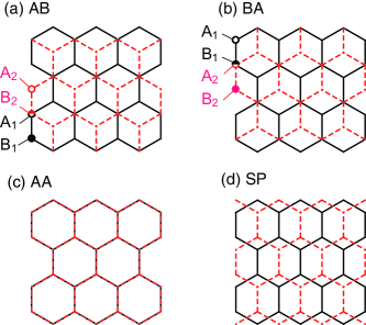
In multilayer graphenes, the weak interlayer interaction allows various different stacking configurations, and there often appear the domain structures consisting of different stacking regions. Lui et al. (2010); Ping and Fuhrer (2012); Brown et al. (2012); Hattendorf et al. (2013); Alden et al. (2013) Recent experiment found a novel type of domain boundary in bilayer graphene Brown et al. (2012); Alden et al. (2013) which connects two equivalent, but distinct Bernal-stacking structures referred to AB and BA, which are shown in Fig. 1(a) and (b), respectively. On the boundary, the AB structure is continuously deformed to the BA structure with in-plane distortion.Alden et al. (2013) Theoretically, the electronic band structure of the AB-BA domain boundary was recently calculated in presence of the interlayer asymmetric potential and it was shown that the boundary-localized states emerge inside the asymmetry-induced energy gap. Vaezi et al. (2013); Zhang et al. (2013)
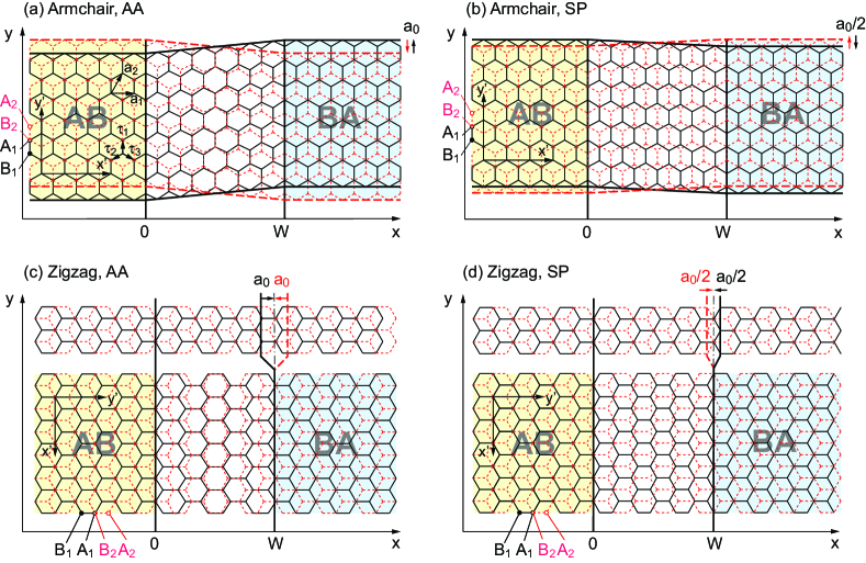
In two-dimensional crystal, a domain boundary significantly influences the electronic transport. There are several theoretical studies investigating the electron transmission through the graphene-based domain structures, such as the grain boundary on polycrystalline graphene Yazyev and Louie (2010) and graphene monolayer-bilayer boundary. Nakanishi et al. (2010); Koshino et al. (2010) In this paper, we calculate the electronic transmission properties across AB-BA domain boundaries in bilayer graphene with no interlayer asymmetry. We consider several specific atomic configurations illustrated in Fig. 2. They are classified into armchair boundary [Figs. 2 (a) and (b)] and zigzag boundary [Figs. 2 (c) and (d)] depending on the orientation of the boundary relative to the honeycomb lattice. Alden et al. (2013) Each case is divided into AA type [Figs. 2 (a) and (c)] and SP type [Figs. 2 (b) and (d)], depending on whether the stacking structure in the intermediate region approximates AA stacking or SP stacking, shown in Fig. 1(c) and (d), respectively.
For each case, we calculate the transmission probability as a function of the incident angle and the electron energy using the effective continuum model. We find that the transmission strongly depends on the boundary structure. Particularly, we show that a low-energy electron easily passes through armchair SP [Figs. 2 (b)], and zigzag AA [Figs. 2 (c)], whereas it is almost completely reflected in armchair AA [Figs. 2 (a)], and zigzag SP [Figs. 2 (d)]. For the latter two cases, the transmission probability sharply rises when the Fermi energy is increased to a certain level. The zigzag boundaries generally have different transmission probability between the two different valleys, offering a possibility to generate the valley polarized current. We show that those characteristic features can be qualitatively understood by considering the local band structure in the intermediate region.
II Formulation
II.1 Atomic structure
We consider the AB-BA domain boundaries on bilayer graphene defined by Figures 2 (a)-(d). In each case, the boundary divides the system into the AB region at left and the BA region at right. We set the axis perpendicularly to the boundary, and axis in parallel to the boundary. We also define the coordinates and fixed to the honeycomb lattice, along the zigzag and armchair directions, respectively. The relation between the two frames is given by for the armchair boundary [Figs. 2 (a) and (b)], and for the zigzag boundary [Figs. 2 (c) and (d)]. We define and as the lattice vectors of graphene, where and are the unit vectors along and , respectively, and is the lattice constant. We also define as the vectors from B site to the nearest A sites as in Fig. 2 (a). We also use nm is the distance between the nearest carbon atoms in graphene.
We define the atomic structure starting from uniform and infinite AB-stacked bilayer graphene. We divide the system into the left (), intermediate () and right regions (), where defines the width of the intermediate region. We fix the AB stacking in the left region, and invert AB stacking in the right region to BA stacking by translating layer 1 and 2 by and , respectively, along direction (armchair direction). The direction of the translation is thus parallel and perpendicular to the boundary in armchair and zigzag boundary, respectively, resulting in shear and tensile lattice distortion, respectively. Alden et al. (2013) The shift is defined as
| (1) |
For the intermediate region, we assume the shift linearly scales in proportion to . The system is translationally symmetric along direction.
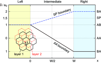
The width of the intermediate region in the real system is estimated at about 10 nm, Alden et al. (2013) and much larger than the atomic scale. The local lattice structure near every single point then approximates a bilayer graphene with a uniform displacement. Let us define as the interlayer displacement vector of layer 2 with respect to layer 1 starting from AA stacking, as illustrated in inset of Fig. 3. In the present systems, is parallel to and depend only on , so that it is written as . is given for the AA type boundary by,
| (2) |
and for the SP type boundary,
| (3) |
which are plotted in Fig. 3. The AA type boundary has the AA-stacked region () at , where the two honeycomb lattices completely overlap. The SP boundary has the structure called SP (saddle point) stacking () at , where is located at the midpoint between the nearest sites. Experimentally, SP type boundary is more stable than AA type boundary because AA stacking is energetically unfavorable. Alden et al. (2013) The total van der Waals energy of SP stacking is between AA stacking and AB stacking, and located at the saddle point on the total energy map as a function of . Popov et al. (2011); Alden et al. (2013)
II.2 Effective continuum model
We derive the effective continuum Hamiltonian for AB-BA boundary from the tight-binding model for atomic orbitals, using a similar approach developed for rotationally stacked bilayer graphene. Moon and Koshino (2013) The Hamiltonian for the tight-binding model is written as
| (4) |
where and represent the lattice point and the atomic state at site , respectively, and is the transfer integral between the sites and . We adopt an approximation, Nakanishi and Ando (2001); Uryu (2004); Trambly De Laissardière et al. (2010); Slater and Koster (1954); Moon and Koshino (2012, 2013)
| (5) |
where is the transfer integral between the nearest-neighbor atoms of monolayer graphene, is that between vertically located atoms on the neighboring layers, and is the interlayer spacing. is the decay length of the transfer integral, and is chosen as so that the next nearest intralayer coupling becomes . The transfer integral for is exponentially small and can be safely neglected.
The low-energy spectrum of the monolayer graphene is given by effective Dirac cones centered at and points, McClure (1956); DiVincenzo and Mele (1984); Semenoff (1984); Shon and Ando (1998); Ando (2005) which are given by . We express the low-energy states of the system in terms of the monolayer’s bases in the vicinity of points. It is written as and
where is the layer index. Here and are envelope functions, which are slowly varying in the atomic scale.
When is much larger than the lattice constant, the interaction between the two graphene layers is dominated by the long-wavelength components. Then the states near the valley and those near are not hybridized and we may consider two valleys separately in constructing the Hamiltonian. The effective Hamiltonian for is written as
| (7) |
where
| (8) | |||||
is the effective Hamiltonian of monolayer graphene McClure (1956); DiVincenzo and Mele (1984); Semenoff (1984); Shon and Ando (1998); Ando (2005), where , is the valley index corresponding to , and is the band velocity of the Dirac cone, which is given in the present tight-binding parameterization as Moon and Koshino (2013)
| (9) |
The matrix describes the interlayer interaction in bilayer graphene shifted by a constant displacement . The function is defined by Moon and Koshino (2013)
| (10) |
where is the unit vector perpendicular to graphene. In the effective Hamiltonian, we substitute for in , i.e., neglect the -dependent terms in the interlayer coupling. In AB (Bernal) stacked graphene, this simplification corresponds to neglecting the trigonal warping and the electron hole asymmetry, corresponding to the band parameters called and . McCann and Fal fko (2006); Koshino and Ando (2009)
The function is smoothly varying function in , and it is approximately written in terms of a few Fourier components as
| (11) |
where is the reciprocal lattice vector satisfying and . In the present choice of the tight-binding parameters, we have . In the following calculation, we scale the energy in units of , and the wavenumber in units of , so that the result does not depend on the values of and . When , in particular, Eq. (11) becomes
| (12) |
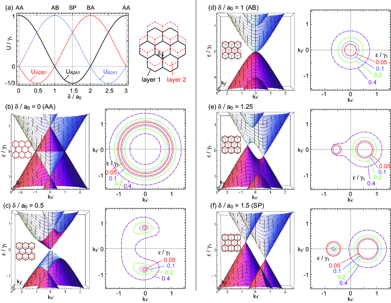
which are plotted against in Fig. 4 (a). The shifts , and correspond to AA, AB, SP and BA stacking, respectively, where , ,, , respectively.
The matrix in Eq. (7) describes the effect of the lattice distortion Suzuura and Ando (2002). Here is given for by
| (13) |
and otherwise, where is defined in Eq. (1). represents the shift of Dirac point in the wave space. The direction of the shift is opposite between the two layers, and it is always parallel to the domain boundary ( direction). As increases, the effect of becomes relatively unimportant compared to the interlayer interaction , since in decreases as while is always of the order of . At nm, for example, is of the order of so that the electronic property is primarily determined by .
II.3 Electron transmission
The electron transmission through the boundary can be obtained by using the transfer matrix. Ando (1991); Cheianov and Fal’ko (2006) The effective Hamiltonian in Eq. (7) can be written as
| (14) |
with certain matrices and , where may depend on the position and is a constant matrix. Since the system is translationally symmetric along direction, is replaced with the quantum number . The Schrödinger equation, , is transformed as a one-dimensional differential equation,
| (15) |
where is the four-component wavefunction, and
| (16) |
The transfer matrix is defined by
| (17) |
Using Eqs. (15) and (17), the differential equation for the transfer matrix is given by
| (18) |
We obtain the transfer matrix connecting the left region and the right region by numerically integrating Eq. (18).
In the AB-stacked region in and the BA-stacked region in , the system is uniform and becomes independent of . In each region, the solution of Eq. (15) can be written as a linear combination of , where and are the eigen values and eigen vectors of the matrix , respectively. The four eigen values are identical in AB and BA regions and written as
| (19) |
where two plus-minus signs give four possible combinations. The corresponding eigen state is a traveling mode when is purely imaginary, while it is an evanescent mode otherwise. The four eigen values consist of two right-going modes and two left-going modes, where a right-going mode can be a traveling mode with velocity in the positive direction, or an evanescent mode decaying in the positive direction.
Let the right-going modes and the left-going modes. The wavefunction at is written as
| (20) | |||||
where is the eigenvector in the AB-region corresponding to , and is the amplitude. Similarly, wavefunction at is written as
| (21) |
where is the eigenvectors in the BA-region. The scripts and represent the left (AB) region and the right (BA) region, respectively. The matrices and are not unitary in general when they include evanescent modes.
Using Eqs. (17), (20) and (21), we obtain an equation connecting the left and right wave amplitudes,
| (22) |
We write this in the form,
| (23) |
where etc., and ’s are block matrices. By sorting the wave amplitudes into in-coming modes, and , and out-going modes, and , we obtain
| (24) |
describes the transmission probability from the in-coming channel to out-going channel .
III Bilayer graphene with constant displacement
In the large limit where is slowly varying in position, the local electronic structure at every single point can be approximately described by the electronic spectrum of uniform bilayer graphene with constant . The -dependent band structure intuitively explains the transmission properties of AB-BA boundary as shown later. In the literature, the effect of interlayer sliding on the band structure was studied for the cases in the vicinity of AB stacking. Mucha-Kruczyński et al. (2011); Son et al. (2011) For the present purposes, we consider the band structure in all the range of the displacement along to cover AB, AA and SP. Fig. 4 (b)-(f) show the band dispersion near point for several ’s along AA-AB-SP line, obtained from Eq. (7) with constant and . In each figure, the left panel shows the surface plot of the energy band in , and the right panel the contour plot at several energies. The spectrum of are obtained by replacing with .
At [AA stacking, Fig. 4 (b)] Ho et al. (2006); Lee et al. (2008); Liu et al. (2009), the energy spectrum consists of four bands expressed by
| (25) |
where , , and . This represents two pairs of Dirac cones shifted by in energy, which intersect at with a Fermi circle of radius . When is increased from 0, the band anticrossing occurs at the intersection, while a pair of band touching point remains on axis on the zero energy plane. For , the touching position is given by
| (26) |
At [AB stacking, Fig. 4 (d)], the split Dirac points merge at the origin, giving the hyperbolic dispersion expressed by, McCann and Fal fko (2006); Koshino and Ando (2009)
| (27) |
When exceeds 1, the band touching point again split but now along axis, and also shift in energy as shown in [Fig. 4(e)]. At [SP stacking, Fig. 4(f)], the spectrum is separated into two Dirac cones shifted in axis the and energy axis, which are given by
| (28) |
The spectrum of is equivalent to that of while the roles of and sublattices are swapped, and thus the spectra from to is identical those from to . The band structure is periodic in with period of .
The conduction band and the valence band are never separated by an energy gap in any value of , and this is because both the spatial inversion symmetry and the time-reversal symmetry remain unbroken in . The robustness of the band touching point in presence of the two symmetries was discussed for several graphene-based systems Mañes et al. (2007), and it can also be explained for general systems using the Berry phase argument, as shown in Appendix A.
IV Results and Discussion
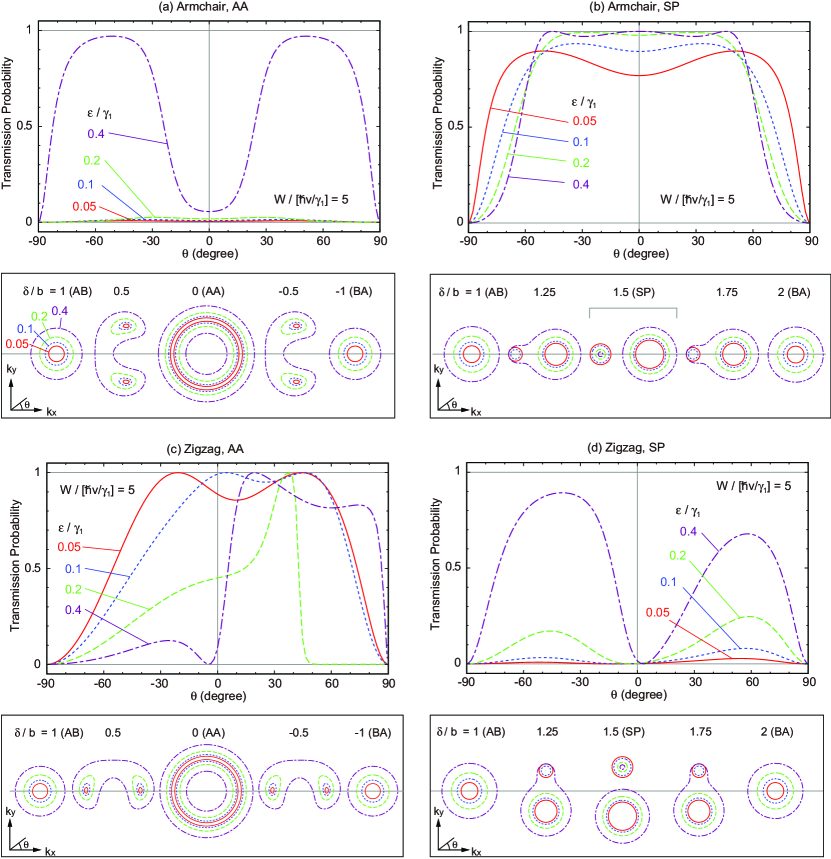
We calculate the electron transmission probability for the AB-BA boundaries of Figure 2(a)-(d). For the width of the boundary, we assume nm to simulate the experimental situation Alden et al. (2013), and this is about ten times larger than the schematic diagram in Fig. 2. We consider the electron energy range , where we have a single Fermi circle of the radius in the left and right regions. We assume that an electron enters the intermediate region from the left with energy and angle , with the initial wavevector . Since the transverse wavevector is preserved throughout the scattering process, the electron transmits to the right region with the same angle with the probability , or reflects back to the left region with the angle with the probability .
Figs. 5(a)-(d) show the transmission probability through the domain boundaries of Figs. 2(a)-(d), respectively, for electron with several different energies. In the armchair boundaries [Fig. 5 (a),(b)], is symmetric with respect to due to the rotation symmetry about axis (zigzag direction), and becomes identical in and . In the zigzag boundary [Fig. 5 (c),(d)], is generally asymmetric, and at is equal to at . This is because the zigzag boundary is symmetric with respect to the reflection about axis (armchair direction), which interchanges and .
The transmission strongly depends on the boundary structure. In the low energy , an electron well passes in armchair SP [Fig. 5(b)] and zigzag AA [Fig. 5(c)], while it is almost completely reflected in armchair AA [Fig. 5(a)] and zigzag SP [Fig. 5(d)]. These features can be roughly understood by considering the local electronic band structure of fixed discussed in Sec. III, which is presented in the lower panel in each of Figs. 5(a)-(d). In the armchair AA, the low-energy Fermi circle splits along direction and it prevents the electron transmission because there are no intermediate matching the initial . In the armchair SP, on the other hand, the electron well transmits because the Fermi circle splits in direction in this case, so that the electron can travel keeping the initial . In the zigzag boundaries [Fig. 5(c),(d)], the direction of the Fermi surface splitting is rotated by so that the properties of the AA type and SP type are interchanged.
The transmission sensitively depends on the electron energy in accordance with the change of the Fermi surface. In the armchair AA, the transmission is suddenly switched on when the energy is increased to as large as . In the band structure, correspondingly, the Fermi circles in the intermediate region begin to overlap with the initial Fermi circle in the AB region. In the zigzag SP [Fig. 5 (d)], similarly, rises in increasing energy as the Fermi circle overlap becomes significant. The transmission probability remains small around , and this corresponds to the absence of electronic states near in the intermediate region due to the Fermi circle splitting. The correspondence between the transmission and the band structure at fixed is intuitive but only approximate, because the local band structure is not well-defined in a finite , and also the lattice distortion gives some shift of the Dirac cone.
These characteristic features of the AB-BA boundary can be exploited to control the electronic transport. Particularly, the armchair AA [Fig. 5(a)] and zigzag SP [Fig. 5 (d)] have a striking property that the electron transmission is almost zero near the charge neutral point, and it sharply rises when the Fermi energy is increased to a certain level. This suggests that the electric current through the AB-BA boundary can be controlled by the field effect through a single gate electrode.
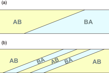
The zigzag boundaries generally have different transmission probability between and valleys, and it is possible in principle to generate the valley polarized current. Similar valley-selective mechanism was previously proposed for the graphene monolayer-bilayer junction Nakanishi et al. (2010), and also for bilayer graphene with spatially modulated gate-electric field Schomerus (2010). Now, the transmission probability of and that of through a zigzag boundary have opposite angle dependence, and , respectively. In the zigzag AA [Fig. 5(c)], at is significant only in , so that transmitted electrons are nearly polarized to in , and to in . The valley polarized current can be generated by an electronic channel obliquely crossing the boundary, as illustrated in Fig. 6(a). The polarization should be enhanced by in multiple boundaries as in shown Fig. 6(b). There the transmission probability from BA to AB is identical to that form AB to BA, because they are just related by interchanging the top and the bottom layers.
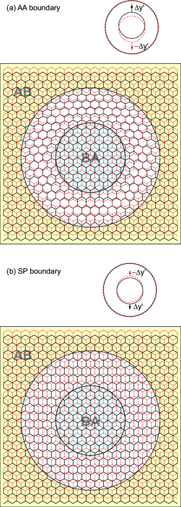
While we concentrated on the boundaries parallel to the zigzag direction or the armchair direction in the present work, AB-BA boundary can occur along any crystallographic direction. Fig. 7 shows AB-BA island structures separated by (a) AA type boundary and SP type boundary, where we translate the layer 1 and 2 inside the inner circle by and [defined in Eq. (1)], respectively, while keeping the AB structure outside the outer circle. In each case, we see that the armchair boundary continuously transforms into the zigzag boundary as moving along the circumference. For a boundary along the intermediate direction between armchair and zigzag, we can calculate the transmission probability in the same theoretical basis, by rotating the crystal axis with respect to in the effective Hamiltonian, Eq. (7). We expect the transmission probability continuously changes as a function of the boundary angle, to interpolate the armchair and zigzag results.
V Conclusion
We studied the electron transmission properties for AB-BA domain boundary in bilayer graphene. Assuming several specific boundary structures, we calculate the electron transmission probability as a function of the electron energy and the incident angle. We find that the transmission strongly depends on the boundary structure. In low-energy region, particularly, the boundary is almost insulating in armchair AA and zigzag SP while it is highly transparent in armchair SP and zigzag AA. In insulating cases, the transmission probability sharply rises when the Fermi energy is increased to a certain level. The zigzag boundaries generally have different transmission properties between and valleys due to the symmetrical reason, and this offers a possibility to generate the valley polarized current. The characteristic features of the electron transmission can be qualitatively understood by the intermediate local band structure which continuously changes across the boundary. In particular, the transport gap in armchair AA and zigzag SP is explained by the the wavenumber mismatch in the Fermi surface of the intermediate region.
ACKNOWLEDGMENTS
We thank A. W. Tsen and P. Kim for helpful discussion. This project has been funded by Grant-in-Aid for Scientific Research No. 24740193 from Japan Society for the Promotion of Science (JSPS).
Appendix A Robustness of Dirac points
Here we show that the band touching point never disappears in presence of the spatial inversion symmetry (SI) and the time-reversal symmetry (TR). We consider a general periodic system, and take a Bloch eigenstate . The Berry curvature is defined as
| (29) |
with a vector field in -space,
| (30) |
In presence of TR symmetry and SI symmetry, we immediately find that at any non-degenerate points, because TR and SI require and , respectively Haldane (2004); Fu and Kane (2007)
We define the Berry phase for a closed path on the -space as,
| (31) |
By using the Stokes theorem, this is transformed as
| (32) |
where is the -space area enclosed by . In TR and SI symmetry, can be non-zero only when includes a band degeneracy point inside, because otherwise vanishes everywhere on . In a massless Dirac Hamiltonian, for example, around the Dirac point is .
If we have a single degenerate point around which is nonzero, the band touching cannot be resolved in any perturbations which keep TR, SI, and the original translational symmetry (i.e., different -points are not coupled). This is because, if an infinitesimal perturbation splits the band degeneracy, the nonzero Berry phase around this point should immediately jump to zero because there are no degeneracy points inside any more, but this is obviously impossible because the the change of the wave function on the path is also infinitesimal. A band gap can open only when a pair of degeneracy points having opposite Berry phases and meet and annihilate at a single -point.
References
- Lui et al. (2010) C. H. Lui, Z. Li, Z. Chen, P. V. Klimov, L. E. Brus, and T. F. Heinz, Nano Lett. 11, 164 (2010).
- Ping and Fuhrer (2012) J. Ping and M. S. Fuhrer, Nano Lett. 12, 4635 (2012).
- Brown et al. (2012) L. Brown, R. Hovden, P. Huang, M. Wojcik, D. A. Muller, and J. Park, Nano Lett. 12, 1609 (2012).
- Hattendorf et al. (2013) S. Hattendorf, A. Georgi, M. Liebmann, and M. Morgenstern, Surf. Sci. 610, 53 (2013).
- Alden et al. (2013) J. S. Alden, A. W. Tsen, P. Y. Huang, R. Hovden, L. Brown, J. Park, D. A. Muller, and P. L. McEuen, PNAS 110, 11256 (2013).
- Vaezi et al. (2013) A. Vaezi, Y. Liang, D. H. Ngai, L. Yang, and E.-A. Kim, Phys. Rev. X 3, 021018 (2013).
- Zhang et al. (2013) F. Zhang, A. H. MacDonald, and E. J. Mele, PNAS 110, 10546 (2013).
- Yazyev and Louie (2010) O. V. Yazyev and S. G. Louie, Nature materials 9, 806 (2010).
- Nakanishi et al. (2010) T. Nakanishi, M. Koshino, and T. Ando, Phys. Rev. B 82, 125428 (2010).
- Koshino et al. (2010) M. Koshino, T. Nakanishi, and T. Ando, Phys. Rev. B 82, 205436 (2010).
- Popov et al. (2011) A. M. Popov, I. V. Lebedeva, A. A. Knizhnik, Y. E. Lozovik, and B. V. Potapkin, Phys. Rev. B 84, 045404 (2011).
- Moon and Koshino (2013) P. Moon and M. Koshino, Phys. Rev. B 87, 205404 (2013).
- Nakanishi and Ando (2001) T. Nakanishi and T. Ando, J. Phys. Soc. Jpn. 70, 1647 (2001).
- Uryu (2004) S. Uryu, Phys. Rev. B 69, 075402 (2004).
- Trambly De Laissardière et al. (2010) G. Trambly De Laissardière, D. Mayou, and L. Magaud, Nano Lett. 10, 804 (2010).
- Slater and Koster (1954) J. Slater and G. Koster, Phys. Rev. 94, 1498 (1954).
- Moon and Koshino (2012) P. Moon and M. Koshino, Phys. Rev. B 85, 195458 (2012).
- McClure (1956) J. McClure, Phys. Rev. 104, 666 (1956).
- DiVincenzo and Mele (1984) D. DiVincenzo and E. Mele, Phys. Rev. B 29, 1685 (1984).
- Semenoff (1984) G. Semenoff, Phys. Rev. Lett. 53, 2449 (1984).
- Shon and Ando (1998) N. H. Shon and T. Ando, J. Phys. Soc. Jpn. 67, 2421 (1998).
- Ando (2005) T. Ando, J. Phys. Soc. Jpn. 74, 777 (2005).
- McCann and Fal fko (2006) E. McCann and V. I. Fal fko, Phys. Rev. Lett. 96, 086805 (2006).
- Koshino and Ando (2009) M. Koshino and T. Ando, Solid State Commun. 149, 1123 (2009).
- Suzuura and Ando (2002) H. Suzuura and T. Ando, Phys. Rev. B 65, 235412 (2002).
- Ando (1991) T. Ando, Phys. Rev. B 44, 8017 (1991).
- Cheianov and Fal’ko (2006) V. V. Cheianov and V. I. Fal’ko, Phys. Rev. B 74, 041403 (2006).
- Mucha-Kruczyński et al. (2011) M. Mucha-Kruczyński, I. L. Aleiner, and V. I. Fal’ko, Phys. Rev. B 84, 041404 (2011).
- Son et al. (2011) Y.-W. Son, S.-M. Choi, Y. P. Hong, S. Woo, and S.-H. Jhi, Phys. Rev. B 84, 155410 (2011).
- Ho et al. (2006) J.-H. Ho, C.-L. Lu, C.-C. Hwang, C.-P. Chang, and M.-F. Lin, Phys. Rev. B 74, 085406 (2006).
- Lee et al. (2008) J.-K. Lee, S.-C. Lee, J.-P. Ahn, S.-C. Kim, J. I. Wilson, and P. John, J. Chem. Phys. 129, 234709 (2008).
- Liu et al. (2009) Z. Liu, K. Suenaga, P. J. Harris, and S. Iijima, Phys. Rev. Lett. 102, 015501 (2009).
- Mañes et al. (2007) J. L. Mañes, F. Guinea, and M. A. Vozmediano, Phys. Rev. B 75, 155424 (2007).
- Schomerus (2010) H. Schomerus, Phys. Rev. B 82, 165409 (2010).
- Haldane (2004) F. Haldane, Phys. Rev. Lett. 93, 206602 (2004).
- Fu and Kane (2007) L. Fu and C. L. Kane, Phys. Rev. B 76, 045302 (2007).