Three-dimensional emission from organic Fabry-Perot microlasers
Abstract
We measured the far-field emission patterns in three dimensions of flat organic dye microlasers using a solid angle scanner. Polymer-based microcavities of ribbon shape (i.e., Fabry-Perot type) were investigated. Out of plane emission from the cavities was observed, with significant differences for the two cases of resonators either fully supported by the substrate or sustained by a pedestal. In both cases, the emission diagrams are accounted for by a model combining diffraction at the cavity edges and reflections from the substrate.
The integration of optical technologies and microelectronics is one of the key areas in current photonics research Matsko (2009), in particular regarding micro-sources. An important aspect for applications is the directionality of the emission from microlasers (see for instance Ref.Yu, Wang, and Capasso (2012)). Many experiments with and simulations of flat microresonators with a thickness much smaller than their horizontal extension investigate only the emission in the plane of the cavity Gmachl et al. (1998); Harayama et al. (2003); Chern et al. (2003); Kurdoglyan et al. (2004); Ben-Messaoud and Zyss (2005); Wiersig and Hentschel (2006); Lebental et al. (2007a); Song et al. (2011). Such microresonators can be easily fabricated on chip using lithography techniques Lebental et al. (2006). Since, however, the thickness of the resonators is of the order of the wavelength, diffraction occurs at the edges of the vertical side walls, possibly leading to emission out of the plane of the cavities. This has seldom been investigated experimentally Peter et al. (2007); Kim et al. (2007); Lee et al. (1998); Renner et al. (2006) or theoretically Ikegami (1972); vuk (1999), however. In order to measure the emission in all three dimensions, we have constructed a solid angle scanner Kim et al. (2007), a setup allowing for the variation of both the azimuthal and polar angle of observation. We used it to investigate organic solid-state microlasers based on dye-doped polymers which can be fabricated easily down to nanoscale resolution Lebental, Bogomolny, and Zyss (2009). Their spectral and emission properties have been intensively investigatedBogomolny et al. (2011); Schwefel et al. (2004); Gozhyk et al. (2012) and depend sensitively on the cavity shape. Here we used ribbon-shaped Fabry-Perot (FP) cavities that are one of the simplest types of microlasers. Their 3D far-field emission was measured and interpreted by an analytical modelPeter et al. (2007); Lee et al. (1998) that is simpler than previously proposed onesIkegami (1972). Reflections at the substrate add complexity to the emission patternsHarayama (2012); Peter et al. (2007). Therefore experiments were carried out with cavities either supported by a pedestal Lozenko et al. (2012) or fully in contact with the substrate. In both cases, a good agreement with the model is obtained, which can be further extended to other resonator shapes.
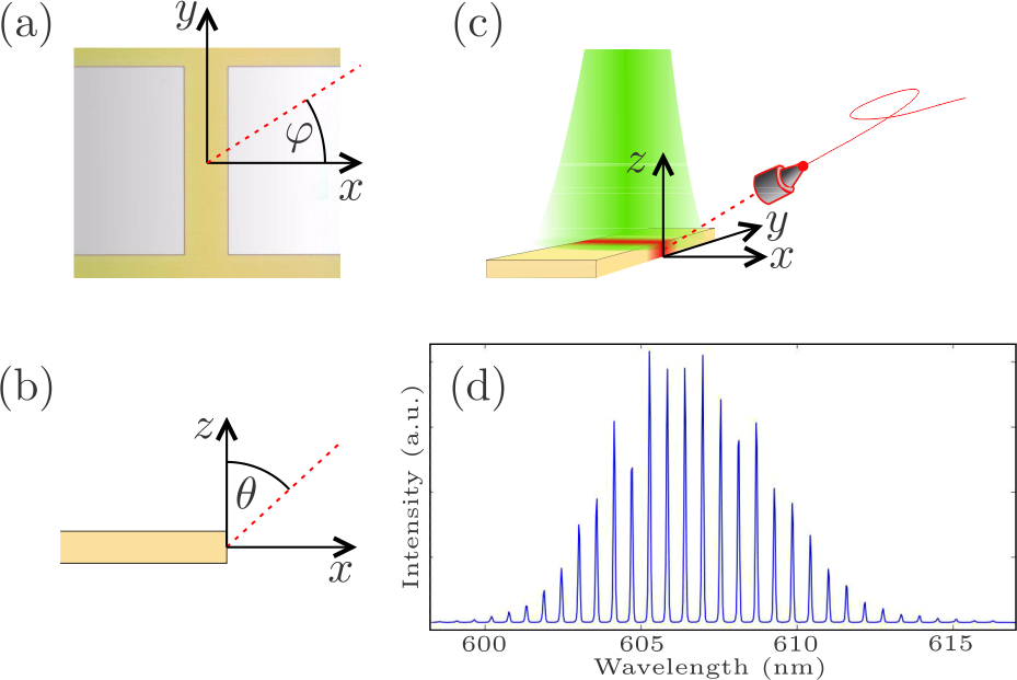
The microlasers were fabricated as follows. A thin layer ( nm) of poly(methylmethacrylate) (PMMA) doped with 5% wt. of the laser dye DCM1114-(Dicyanomethylene)-2-methyl-6-(4-dimethylaminostyryl)-4H-pyran is spin-coated on a silicon wafer with a m thick layer of silica. The cavity structures are then created using electron beam lithography, which ensures vertical sidewalls and sharp edges with sub-wavelength accuracy. A photo of a ribbon-shaped cavity with a width of m is shown in Fig. 1(a). In order to produce cavities supported by a pedestal, the samples were dipped in hydrofluoric acid so as to partly under-etch the silica layer beneath the polymer cavities without damaging the organic part Lozenko et al. (2012).
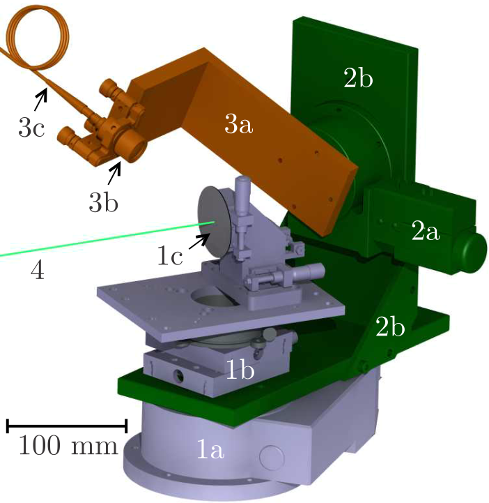
The microlasers were pumped just above their lasing threshold by a frequency-doubled Nd:YAG laser ( nm, ps, Hz) with linear polarization parallel to the y axis [see Fig. 1 (c) for notations and Ref.Gozhyk et al. (2012)]. The emission from the cavity into arbitrary directions was collected with a lensed fiber and transferred to a spectrometer. A typical measured spectrum is shown in Fig. 1(d). The sample holder itself does not move with respect to the table, whereas the collection lens is positioned by two rotating arms as shown in Fig. 2. To ensure that the cavity stays aligned with the lens, the two motors rotating the arms must have a very small eccentricity (m for Newport RV120PP rotation stages), and their axes must cross each other with a mismatch tolerance of the order of m. The latter was achieved via precise manufacturing of the arms and assembling them with centering pins. The wafer with the microlasers was attached vertically to the setup so that the horizontal pump beam is perpendicular to the wafer.
Previous studies demonstrated that many properties of flat microlasers like their spectra can be explained in the framework of a 2D effective refractive index approximation Lebental et al. (2007b). Just above threshold, ribbon (FP) cavities exhibit only one kind of lasing modes that is based on the bouncing-ball orbit along the direction. Feedback along the direction is suppressed because photons travelling in that direction are lost in the polymer layer [cf. Fig. 1(a)]. Consequently, FP cavities emit only in the and directions Lebental et al. (2007b). Therefore, we measured the latitude emission diagram, that is the far-field lasing intensity with respect to the polar angle at fixed . The latitude emission diagram for a cavity on a pedestal is shown in Fig. 3. There is no significant dependence on the angle of the spectral and polarization features of the emission, unlike the cases reported in Ref.Kim et al. (2007). The major part of the lasing emission is not mainly in the cavity plane () as could have been expected, but mostly out of the plane of the cavity. Moreover, the emission diagram exhibits an oscillating pattern that does not depend on the FP width.
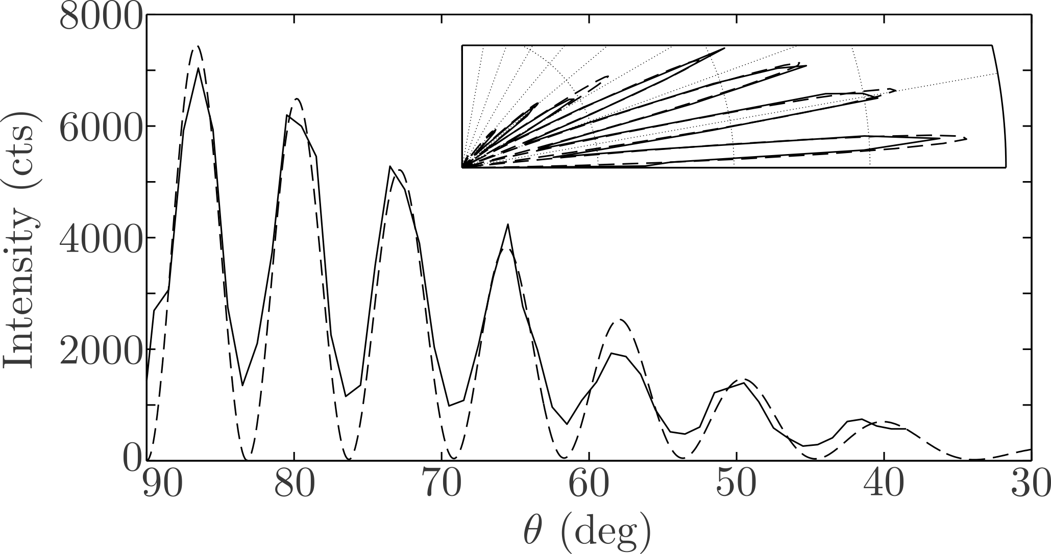
In fact, the observed emission pattern originates from two different effects, namely reflections at the substrate and diffraction at the cavity edges. It can therefore be expressed as a product of two terms Peter et al. (2007),
| (1) |
The factor results from the interference between the direct ray trajectory from the sidewall to the lens and the one reflected at the silicion wafer as shown in Fig. 4(a).
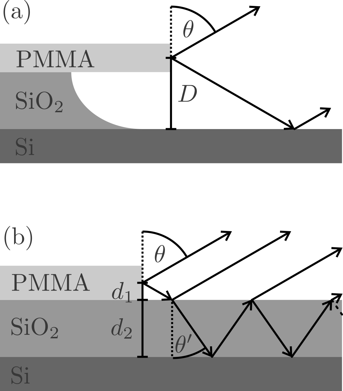
It has the form Peter et al. (2007)
| (2) |
where is the distance between the silicon surface and the center of the polymer layer [see Fig. 4(a)], is the wave number, and is the Fresnel reflection coefficient at the air/silicon interface for s polarization since the FP microlaser emits light polarized in the cavity plane Gozhyk et al. (2012). This term is responsible for the oscillatory behavior that dominates the emission pattern. The second factor, , is related to the diffraction at the edges and determines the envelope of the emission pattern. It is the Fourier transform (FT) of the electric near-field distribution at the cavity side wall Lee et al. (1998), which is, however, not known a priori. For the sake of simplicity it is assumed that the near field is homogeneous over a certain length which is of the order of the cavity thickness. The resulting diffraction pattern is therefore that of a slit, namely,
| (3) |
This factor provides the envelope of the latitude diagram whose behavior is dominated by the oscillatory factor . Therefore, the exact shape of cannot be determined here.
A fit of this model is plotted as dashed line in Fig. 3 and shows very good agreement. The fitted parameters are m and nm, where was used for the refractive index of silicon. The thicknesses of the polymer and silica layers were measured with a profilometer to be nm and m, respectively. As expected, the value of is of the order of the thickness of the polymer layer. The measured thicknesses correspond to a value of m, from which the fitted value deviates by less than .
The latitude emission diagram for a FP cavity fully supported by the silica coated substrate is shown in Fig. 5.
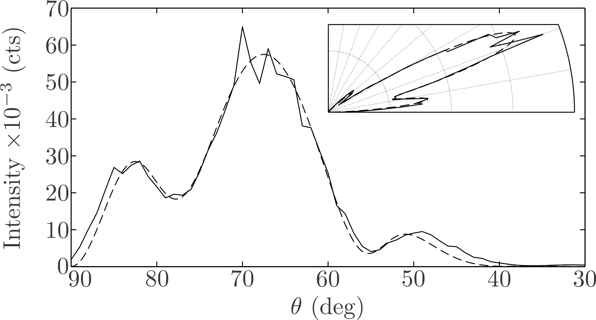
The main emission direction is obviously out of the plane and concentrated around with two smaller lateral lobes around and . The interference pattern is more complicated here since the direct trajectory interferes with one reflected at the air-silica interface and an infinite number of reflections at the silica-silicon interface as depicted in Fig. 4(b). Adding up all trajectories results in
| (4) |
with , , and with . The Fresnel reflection and transmission coefficients for angle of incidence and s polarization are denoted by and , respectively, where I stands for the air/silica, II for the silica/air and III for the silica/silicon interface. The fit parameters are , which is half the thickness of the cavity, , which is the thickness of the silica layer [see Fig. 4(b)], and . The fit (dashed line in Fig. 5) shows very good agreement with the measurement for parameters nm, m, and nm. It should be noted that the shape of the latitude emission diagram depends sensitively on the parameters and . The measured thickness of the PMMA layer is nm, which agrees well with the fitted values for and . The thickness of the silica layer, m like for the pedestal sample, also agrees well with .
In summary, we have investigated flat organic microlasers and observed emission out of the cavity plane with a solid angle scanner. For ribbon-shaped cavities, the measured latitude emission diagrams were compared to a simple analytical model taking into account diffraction at the cavity edges and reflections from the substrate, showing excellent agreement. The methodology applied here can be generalized to other, more complicated cavity shapes, and allow an insight into the mode structure inside the resonator, since the diffraction patterns are related to the electric field distributions at the vertical cavity side walls. These cannot be predicted analytically but contain important information on the cavity modes. They are important to understand the reflection of waves at such interfaces with finite height Ikegami (1972); vuk (1999). For instance, the reflection coefficients for finite interfaces are of great relevance for the determination of lasing thresholds and to improve on the effective refractive index approximation Bittner et al. (2009). In addition, the diffraction pattern is directly connected to the diffraction at dielectric corners and edges, which remains an open problem Gennarelli and Riccio (2011).
S. B. gratefully acknowledges funding from the European Union Seventh Framework Programme (FP7/2007-2013) under grant agreement n∘ 246.556. The authors thank S. Colin for fruitful discussions regarding the design of the solid angle scanner, and M. Boudreau and G. Bader for ellipsometric measurements of refractive indices.
References
- Matsko (2009) A. B. Matsko, ed., Practical Applications of Microresonators in Optics and Photonics (CRC Press, Boca Raton, 2009).
- Yu, Wang, and Capasso (2012) N. Yu, Q. Wang, and F. Capasso, Laser & Photonics Reviews 6, 24 (2012).
- Gmachl et al. (1998) C. Gmachl, F. Capasso, E. E. Narimanov, J. U. Nöckel, A. D. Stone, J. Faist, D. L. Sivco, and A. Y. Cho, Science 280, 1556 (1998).
- Harayama et al. (2003) T. Harayama, T. Fukushima, P. Davis, P. O. Vaccaro, T. Miyasaka, T. Nishimura, and T. Aida, Phys. Rev. E 67, 015207 (2003).
- Chern et al. (2003) G. D. Chern, H. E. Tureci, A. D. Stone, R. K. Chang, M. Kneissl, and N. M. Johnson, Appl. Phys. Lett. 83, 1710 (2003).
- Kurdoglyan et al. (2004) M. S. Kurdoglyan, S.-Y. Lee, S. Rim, and C.-M. Kim, Opt. Lett. 29, 2758 (2004).
- Ben-Messaoud and Zyss (2005) T. Ben-Messaoud and J. Zyss, Appl. Phys. Lett. 86, 241110 (2005).
- Wiersig and Hentschel (2006) J. Wiersig and M. Hentschel, Phys. Rev. A 73, 031802 (2006).
- Lebental et al. (2007a) M. Lebental, J. S. Lauret, J. Zyss, C. Schmit, and E. Bogomolny, Phys. Rev. A 75, 033806 (2007a).
- Song et al. (2011) Q. H. Song, L. Ge, J. Wiersig, J.-B. Shim, J. Unterhinninghofen, A. Eberspächer, W. Fang, G. S. Solomon, and H. Cao, Phys. Rev. A 84, 063843 (2011).
- Lebental et al. (2006) M. Lebental, J. S. Lauret, R. Hierle, and J. Zyss, Appl. Phys. Lett. 88, 031108 (2006).
- Peter et al. (2007) E. Peter, A. Dousse, P. Voisin, A. Lemaître, D. Martrou, A. Cavanna, J. Bloch, and P. Senellart, Appl. Phys. Lett. 91, 151103 (2007).
- Kim et al. (2007) D. K. Kim, S.-J. An, E. G. Lee, and O. Kwon, J. Appl. Phys 102, 053104 (2007).
- Lee et al. (1998) T.-D. Lee, P.-H. Cheng, J.-S. Pan, R.-S. Tsai, Y. Lai, and K. Tai, Appl. Phys. Lett. 72, 2223 (1998).
- Renner et al. (2006) J. Renner, L. Worschech, A. Forchel, S. Mahapatra, and K. Brunner, Appl. Phys. Lett. 89, 091105 (2006).
- Ikegami (1972) T. Ikegami, IEEE J. Quantum Electr. 8, 470–476 (1972).
- vuk (1999) Opt. Quantum Electr. 31 (1999), 10.1023/A:1006978007453.
- Lebental, Bogomolny, and Zyss (2009) M. Lebental, E. Bogomolny, and J. Zyss, in Practical Applications of Microresonators in Optics and Photonics, edited by A. B. Matsko (CRC Press, Boca Raton, 2009).
- Bogomolny et al. (2011) E. Bogomolny, N. Djellali, R. Dubertrand, I. Gozhyk, M. Lebental, C. Schmit, C. Ulysse, and J. Zyss, Phys. Rev. E 83, 036208 (2011).
- Schwefel et al. (2004) H. G. L. Schwefel, N. B. Rex, H. E. Tureci, R. K. Chang, A. D. Stone, T. Ben-Messaoud, and J. Zyss, J. Opt. Soc. Am. B 21, 923 (2004).
- Gozhyk et al. (2012) I. Gozhyk, G. Clavier, R. Méallet-Renault, M. Dvorko, R. Pansu, J.-F. Audibert, A. Brosseau, C. Lafargue, V. Tsvirkun, S. Lozenko, S. Forget, S. Chénais, C. Ulysse, J. Zyss, and M. Lebental, Phys. Rev. A 86, 043817 (2012).
- Harayama (2012) T. Harayama, private communication (2012).
- Lozenko et al. (2012) S. Lozenko, N. Djellali, I. Gozhyk, C. Delezoide, J. Lautru, C. Ulysse, J. Zyss, and M. Lebental, J. Appl. Phys 111, 103116 (2012).
- Note (1) 4-(Dicyanomethylene)-2-methyl-6-(4-dimethylaminostyryl)-4H-pyran.
- Lebental et al. (2007b) M. Lebental, N. Djellali, C. Arnaud, J.-S. Lauret, J. Zyss, R. Dubertrand, C. Schmit, and E. Bogomolny, Phys. Rev. A 76, 023830 (2007b).
- Bittner et al. (2009) S. Bittner, B. Dietz, M. Miski-Oglu, P. Oria Iriarte, A. Richter, and F. Schäfer, Phys. Rev. A 80, 023825 (2009).
- Gennarelli and Riccio (2011) G. Gennarelli and G. Riccio, IEEE Trans. Antennas Propag. 59, 898 (2011).