Artifact-free data recovery system for an ASNOM application
Abstract
A digital signal acquisition system for an Apertureless SNOM (ASNOM) based on a digital signal processing (DSP) card is presented. An electromagnetic wave scattered by an AFM-like tip is initially detected by an optical homodyning in a Michelson interferometer, with a homodyne phase modulation caused by a periodic travel of the reference arm mirror. Utilizing a non-linear dependency of the tip scattering amplitude on a tip-sample separation distance, the non-fundamental components of a tip oscillation frequency are recovered in optical signal within each tip oscillation period. A detected value, corresponding mostly to the near-field modes of a tip-sample electromagnetic interaction, is then averaged over all reference phases. A modular structure of the data acquisition and signal recovery program allows modify easily the modes of operation and the recovery algorithms.
pacs:
07.79.FcI Introduction
An Apertureless Scanning Near-Field MicroscopyZenhausern, O’Boyle, and Wickramasinghe (1994) (ASNOM) gets recently a powerful tool for the optical surface investigations with a lateral resolution of a few nanometerZenhausern, Martin, and Wickramasinghe (1995); Martin, Zenhausern, and Wickramasinghe (1996), regardless to the wavelength being usedKnoll et al. (1997); Hillenbrand, Knoll, and Keilmann (2001). The successful applications of an ASNOM were demonstrated for a nanometer-scale material recognitionKnoll and Keilmann (1999); Wurtz, Bachelot, and Royer (1998), local field mappingKrenn et al. (1999), biological imagingMartin, Zenhausern, and Wickramasinghe (1996); Brehm et al. (2006). ASNOM technique is also successfully implemented for a Raman subwavelength resolution imaging Anderson (2000); Hayazawa et al. (2002).
A wavelength-independent nanometer-scale resolution can be achieved due to the fact that an electromagnetic interaction between a surface feature and a sharp AFM-like tip is caused by the evanescent fields around the tip apex, which decay quickly with a distance. The oscillations of a tip dipolar momentum excited by a local electromagnetic field around the tip are emitted into the environmental space and can be reliably detected with some experimental tricks. A sinusoidal tip oscillation used in a topography feedback system is utilized in an ASNOM, to discriminate fundamentalZenhausern, O’Boyle, and Wickramasinghe (1994) or, later, higher Labardi, Patanè, and Allegrini (2000); Hillenbrand, Knoll, and Keilmann (2001) harmonic components of a tip oscillation frequency in an optical signal. It is commonly accepted now, that a strong non-linearity of the tip-surface near-field interaction dependency on the tip-surface distance should be used to detect the higher harmonics in a detector output, mainly consisting of an ASNOM signal. In first ASNOMs, the analog era single-frequency lock-in systems were usedZenhausern, Martin, and Wickramasinghe (1995); Maghelli et al. (2001); Bek, Vogelgesang, and Kern (2006) to detect the desired harmonic components. Last years, a wide variety of the digital signal acquisition and processing systems got available on the market, allowing more sophisticated recovery algorithms. A digital recovery system was proposedOcelic, Huber, and Hillenbrand (2006) to detect a single high harmonic component in a photocurrent.
A clear demand exists, to develop a flexible acquisition system for the ASNOM applications, which can implement different modes of operation: single-wavelength elastic light scattering, tip-enhanced fluorescence microscopy, tip-enhanced Raman mode, ”white light” tip-enhanced Fourier-spectroscopy mode etc. Since an optical signal in a fiber-defined SNOM also depends strongly on a distance between the tip and surface feature, a signal recovery in such application is very similar to one used in apertureless SNOMs. In some applications, a gated photon-counting may be used instead of analog signal processing. To achieve a flexibility, the data processing algorithms in such a system must consist of independent software modules, so that any of them can be easily improved or replaced without losses of a system functionality. Just a few papersBek, Vogelgesang, and Kern (2006); Ocelic, Huber, and Hillenbrand (2006); Esslinger et al. (2012) are devoted to describe an ASNOM signal recovery.
I.0.1 Hardware
In a present paper we report a successful attempt to use a DSP-based signal acquisition card P25MP (25); board (Innovative Integration Inc.). A card is equipped with four ADCs (max. rate 25 MSPS) and four DAC channes (max. rate 50 MSPS), 16-bit resolution each. Parallel ports for a digital input and output are also available on the card. Input-output operations (DACs, ADCs, digital ports) are hardware-controlled with an FPGA logic, and the parameters of its operation (clock frequencies, sampling frame dimensions etc.) can be set by the software. A 300-MHz floating point DSP (TMS320C6713) manages data acquisition, transfer and output.
A signal processing in the recovery system being described herein, occurs in two hardware and software spaces. An input signal sampling as well as analog output control are managed in a hardware/software of the P25M card (further mentioned as target). Math operations over the data having been collected, as well as program-to-user interface, including a parameter control panels and virtual oscilloscopes for a signal visualization are running in an IBM-PC computer (which is mentioned as host in the further text). Finally, the recovered signal value can be sent from a host computer to a target card in order to set appropriate voltages for an analog transfer of a collected signal. For a data packet transfer, a PCI slot on the host motherboard is used, in which a target card is physically plugged in.
For an SPM operation a R9 model SPM controller (RHK, Inc.) was used and a home-made ASNOM scanning headKazantsev and Ryssel (2013). Most of the measurements were carried out with a tunable laser (MERIT-G, Soliton Inc.) running in a CW mode .
I.0.2 ASNOM signal: optical homodyning
There are two key features in a signal recovery of an ASNOM instrument running in elastic mode (in which the wavelength of a scattered light does not change). First, a vanishing light wave scattered by the tip under an influence of an irradiating field can be ”amplified” on a photodetector sensitive pad by optical homodyning or heterodyning (see Fig.1(a)). In the presence of a coherent reference wave, the variations in the photocurrent being detected are proportional to the first power of the scattered wave phasor length (instead of square expected without reference wave). Second feature utilizes a non-linear dependency of the tip scattered wave amplitude on the tip-sample distance. Since it is the main nonlinearity in the system, the higher harmonic components in the photocurrent contain mainly the information concerning an electromagnetic interaction between tip and surface, caused by the fields localized in the gap between the tip and sample.
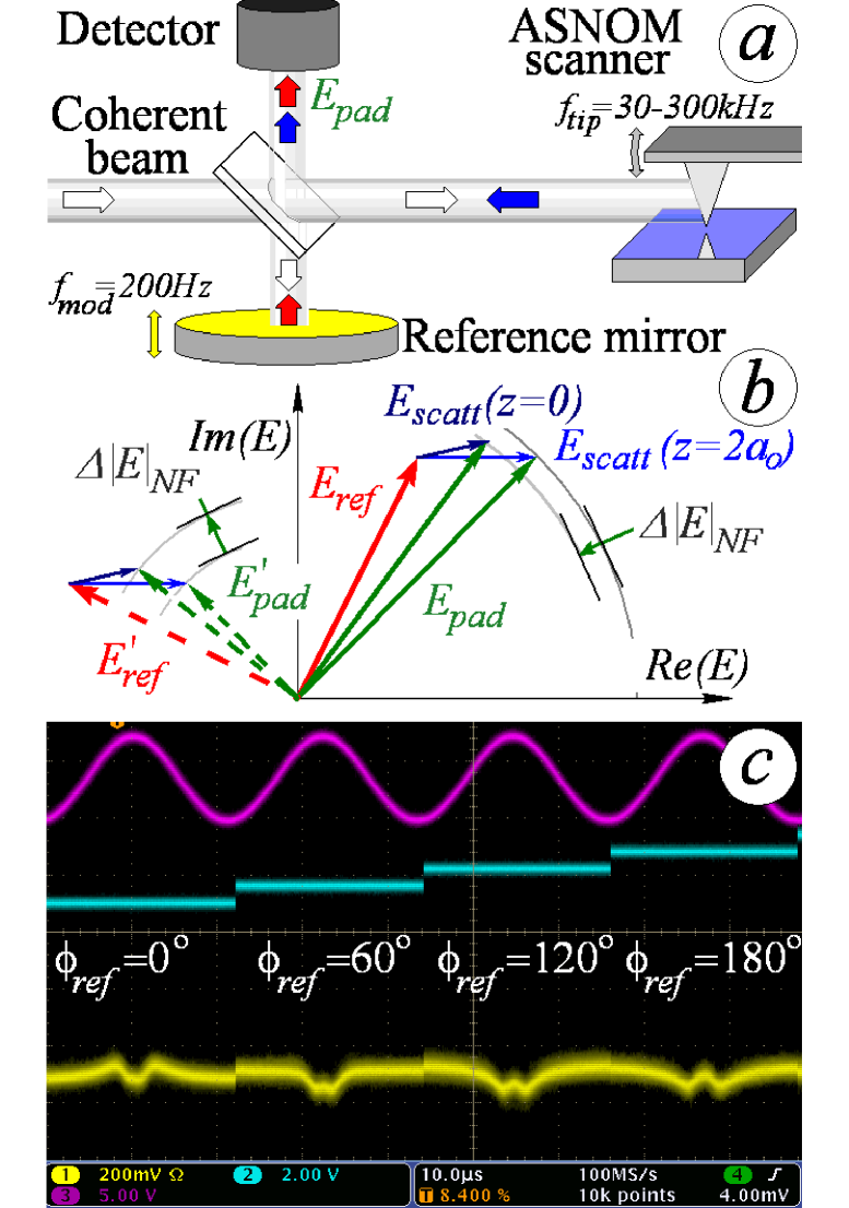
As it is shown in Fig.1(b), a photocurrent signal in an optical homodyne Michelson scheme is determined by a sum of the field phasors. Depending on a reference beam phase, such interference can be constructive or destructive, so that a photocurrent signal may contain positive or negative peaks which appear at the moment when the tip ”bounces” the surface. The traces of a detector output signal, acquired simultaneously with a tip oscillation signal are shown in Fig.1(c) for different reference phases. For each definite reference phase, a near field component can be extracted from the data, and stored as some complex number, representing the amplitude and phase of a feature.
One should keep in mind, that recovery of just a single non-fundamental harmonic (let say second) content is not perfectly adequate to the signal being expected and collected. The near-field-caused pulse in the signal has a Gaussian-like shape, as shown in Fig.1(b). It means that all higher harmonics contain the information together (and their phases must all be acquired precisely), so that a recovery of just a single one means some loss of a useful signal. More careful investigation of this pulse-like photocurrent feature shown in the figure, leads to an observation that not only amplitude of a scattered wave depends on a tip-sample gap, but also a phase: the trace looks as if it was plotted on a side of a cylinder, rotating with a reference mirror displacement. Therefore, to improve a signal to noise ratio, some gated recovery algorithm looks to be better, with a gate shape corresponding to an expected signal shape. It seems useful to make a remark here that a gated photon countingBek, Vogelgesang, and Kern (2006) can be implemented for a signal recovery as well.
Regardless to the near-field pulse recovery algorithm within a single tip oscillation period, an averaging over all possible phases of a reference beam must be provided afterwards, to exclude random nature of a reference arm length. It is clear from the figure, that the oscillations in a photocurrent signal, caused by near-field interaction between tip and surface, must depend on the reference phase in a sinusoidal way:
| (1) |
Thus, to get an adequate measure of a near-field tip-sample interaction, an acquired signal must be averaged over all possible reference beam phases. Most evident wayOcelic, Huber, and Hillenbrand (2006) is to modulate an optical length of a reference arm by a periodic mirror motion and to consider a phase modulation respectively in a recovery math. Another way to average over all reference beam phase is a heterodyne recoveryHillenbrand and Keilmann (2000); Hillenbrand, Knoll, and Keilmann (2001). In this case, a reference field phasor turns on a complex plane around with a rate of a light modulation frequency ( in the papers being cited). A recovery of a signal at this combinational frequency yields a measure of an ASNOM signal, averaged over several turns of a reference phase.
In an assumption that there is completely no artifacts caused by the optical misalignments, and a travel of a reference mirror leads purely to an appropriate turn of the reference field phasor, a reference phase modulation can be simplified by using of just two points of a mirror positionEsteban et al. (2008), shifted with respect to each other for of the phase delay. It leads to an obvious disadvantage: each raster line should be mechanically scanned twice, with different reference phases. Additionally, the operator looses a degree of freedom to discover a misalignment of an interferometer (e.g. by observing a wrong shape of a signal trace on the oscilloscope) before mapping got started.
Therefore, to detect an ASNOM optical signal two math procedures are necessary. First, a non-fundamental response feature in the signal must be recovered within each tip oscillation period, yielding in some complex value. Such a processing we will mean as primary math in a further consideration. Second, the results of primary math must be averaged over full turn of a reference beam phase (keeping in mind the reference beam amplitude turn on a complex plane). Such an operation will be mentioned as secondary math in the further text. It looks to be more-less natural to separate all processing steps, so that any of them took a minimal influence on the other flow stages.
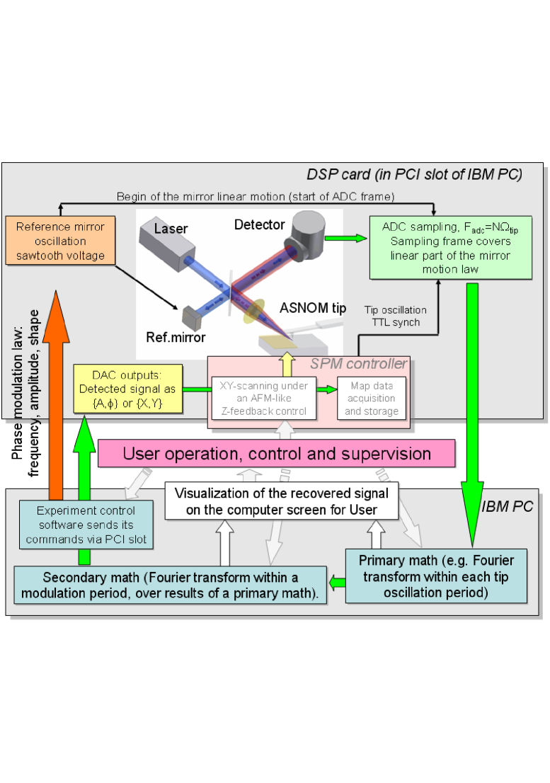
A signal recovery data flow is shown schematically in Fig.2.
II Reference mirror motion control
To provide a phase modulation, a reference mirror should be driven along its axis. If its positioning is described with a sinusoidal law, some unpleasant conditions appear in the game. A phase of a reference beam is determined by the arm optical length in a following way: (a factor of two near variable represents that the light propagates forward and back in the reference arm). In this case, a dependency on time for the reference wave phasor in (1) becomes double-sinusoidal:
| (2) |
It means that, in the case of sinusoidal law of the phase modulation, the data points provided by the primary math are distributed non-uniformly on a phase scale. Their density is higher near the dead points of reference mirror working stroke, and lower in the middle. It makes an utilization of a standard Fourier-transform operation problematic. Additionally, such a non-uniform distribution may lead to appearance of artifacts, caused by enhancement of the noise containing in some data group and suppression of the signal in others. Another solution to overpass that might be a variable ADC sampling rate within a phase modulation period, but it is technically rather hard to manage.
Due to these reasons, a voltage which determines a position of the reference mirror (being applied to the piezo-actuators) must contain a linear part in its oscillation law. In a single-wavelength application, a span of this linear part must correspond to half a wavelength, so that a reference phase makes a full turn during the data acquisition. In a multiple-wavelength applications, with a signal recovery algorithm similar to the Fourier-spectroscopy, the mirror working travel must be naturally much longer than a wavelength used in the experiment.
The sharp shocks at the dead points, corresponding to a motion direction change, may cause parasite axial and angular vibrations of the reference mirror, and spoil an alignment of the interferometer scheme. To avoid that, some smoothing of the oscillation law must be provided for a vicinity of the dead points. Naturally, it enlarges real range of motion, as well as decreases a fraction of time available for the data acquisition. We use a semi-period of a sinusoid, tailored by the derivative to the linear part of the curve.
An array of 16-bit data, corresponding to the desired oscillation law (with appropriate values of amplitude, position offset, dead point smoothing etc.) is transferred by a target CPU to the DAC output queue in a target FPGA. The DAC clock frequency, physically kept by an FPGA circuitry, is also loaded into an appropriate control register of FPGA once at initialization time by the program running in the target CPU. Thus, a signal of appropriate shape and frequency is generated in DAC/FPGA with no further intervention of the target CPU.
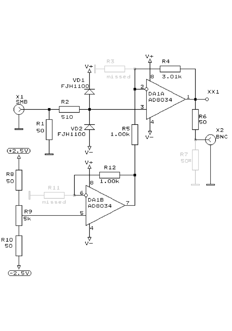
To convert a voltage from (-2.0V…+2.0V) range provided by a P25M card DAC output to a (-12V…+2V) range required by an input of the controller E- (503) which drives a S-316 piezo-positioning stage S-316 (a, b) , a home-made amplifier board was used. It contains four independent stages with adjustable gain and offset each (see Fig.3). To reduce the noises, its power supply is isolated from all nets of the host computer (IA0515D followed by LM7812/LM7912), and its ground is connected just to output jack of the P25M card.
Due to accepted ideology, a new value of a recovered signal gets available once per a mirror oscillation period (half period, if ascending and descending branches of the mirror oscillation law are processed separately). Therefore, a reference mirror oscillation frequency limits a final speed of an ASNOM mapping in the system, and it seems natural to increase it as much as possible. There are, however, two limiting factors. First, the oscillation period of the ASNOM tip must be much shorter than a mirror oscillation time, in order to simplify data processing by an assumption that the reference phase was constant during a tip oscillation period. With a typical resonant frequencies of the tips being used () such a condition seems to be fulfilled if is less than . Second factor is a limited mechanical response rate of the piezo-actuator being used for a mirror positioning. A feedback-enhanced positioning stage S-316 (b) S-316 (Physik Instrumente, GmbH), is claimed to have its first resonance frequency of 5.5 kHz. Nevertheless, a small commercial mirror (PF05-03-M01, Thorlabs) is already too heavy for this stage, reducing the frequency of an artifact-free operation to approx. 120 Hz. Situation can be improved by using of a thick Au-coated piece of a silicone wafer instead of a mirror, but even in that case the shape of the acquired primary signal gets distorted at the frequencies above 220 Hz, indicating most probably an angular misalignment of the interferometer.
III Data acquisition
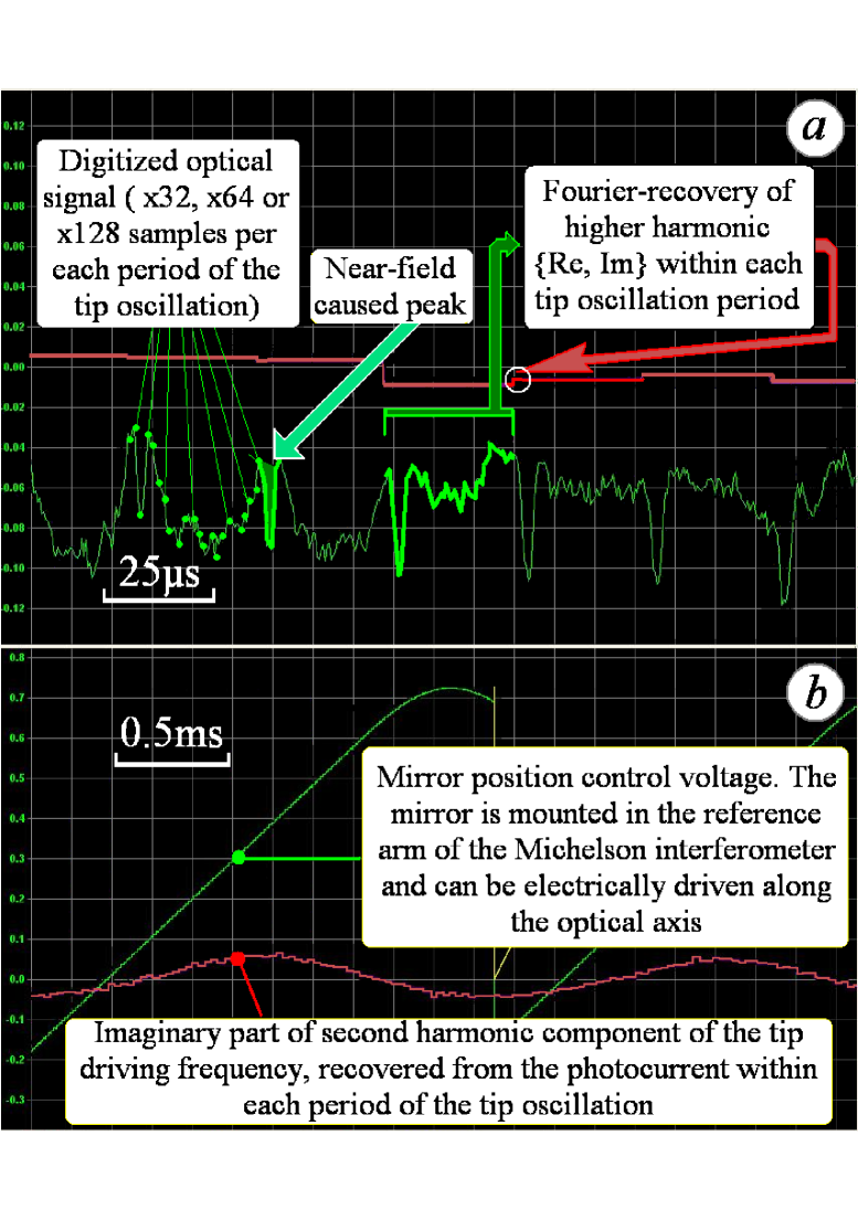
To acquire the data, an ADC channel of the signal acquisition board is used. A sampling frame covers full linear part of the reference mirror motion. As a hardware event to trigger a frame, the edge of the tip oscillation clock (received as a TTL signal from an SPM controller) is used, which comes first after a linear part of the reference mirror is started (software event generated by the mirror control thread in the target space). A sampling rate is set to an exact multiple of , so that each tip oscillation period is covered by 32..128 samples of ADC. Thus, there should be enough data to restore higher harmonic components in the signal.
To avoid an aliasing and/or phase unambiguity in the received data during the whole reference phase turn, an ADC sampling frequency is set to exact multiple of the tip oscillation frequency. The acquisition frame parameters (ADC sampling frequency, logical length of a sampling frame etc.) are stored into the FPGA registers on a target bus once at the initialization time. To be triggered, an acquisition of a new frame requires just a few CPU operations, and produces therefore almost no operational delay in the system.
Another ADC channel is simultaneously used for a sampling of a tip displacement signal, received from an ASNOM scanning head. Nominally, an AFM-like feedback of the SPM controller keeps the conditions of a tip oscillation constant. In a real life, the phase of a tip oscillation can be slightly shifted from its ideal value. It means, that a recovery of an ASNOM pulse in the photocurrent (which occurs just at the moment of the tip-sample ”contact”) can be distorted by a time shift between ideal and real moment of a contact. The system would be especially sensitive to such a time lag in the mode of gated recovery of the signal (which is more promising than a single-harmonic analysis, because it utilizes a whole spectrum of an ASNOM response). The ADC samplings of a tip displacement signal, being controlled by an FPGA circuitry, occur exactly simultaneously with the samplings of an optical signal delivered from a detector.
As soon as data frame is completely acquired in the target, it is sent to the host, via their common PCI-channel.
The third ADC channel of a target card can be used for a control of voltage driving the reference mirror. It allows visualize all relevant processes on the screen of the same virtual oscilloscope in the host computer. It should be kept in mind, however, that a transfer of data acquired also by the second pair of ADC inputs reduces a rate of a PCI channel being used for a communication between a target and a host.
IV ASNOM component recovery within a tip oscillation period (primary math)
After a host receives a new data frame, a recovery of the peaks caused by a near-field effects gets started. A full data frame, acquired for a whole working travel of the reference beam mirror is subdivided before processing into the logical pieces corresponding to a single tip oscillation period each. Since an ADC sampling frequency is set to exactly multiple of a tip oscillation frequency , all periods in the data array are acquired at completely same phase, so that the jitter and aliasing artifacts are suppressed. There is a choice of a recovery algorithms to be used at this step of signal discrimination. First, just a single higher harmonic component can be extracted as a complex number within a period. Second, a detector signal can be multiplied by a gate function, corresponding in time to the moment of a tip-surface touch. Third, the pulses received from a photon counter (in that case a frame of digital port data must be acquired from a target) can also be used as an input data.
Simultaneously to the optical signal recovery, a first harmonic component is calculated in a data set corresponding to a cantilever deflection signal. Ideally, a topography feedback should keep the conditions of a tip oscillation to be constant. In reality, the phase of a deflection suffers of significant fluctuations (), and therefore an exact time of a ”bounce” can be shifted. A measured phase shift of a real tip oscillation law allows to correct a position of a gate function in a gated discrimination, or to correct a phase of output data for a higher harmonic demodulation method.
V Averaging over different phases of a reference beam (secondary math)
Since a reference modulation law was chosen to be linear in a time, an average over the reference beam phase consists simply of a single harmonic calculation in an array of complex numbers containing the results of a primary math. In a simplest case of elastic scattering of the light, a linear part of the mirror oscillation law is set to cover a bit more than a half wavelentgh (full turn of a reference phase), so that a primary math data contain just a single oscillation of a value. Nevertheless, there is no principal limitations to deal with a multiple-period data (in such a case some higher harmonic should be calculated) or even to do full Fourier-transform processing like in a Foruer-spectrometer if the reference mirror covers much more than a single wavelentgh.
Since the reference phasor rotation is opposite for an ascending and descending branches of a reference mirror travel, we subdivide data processing for these branches in two separate jobs. While a target acquires a data for an ascending branch, a host processes the data of descending branch, received before. Once ascending branch data is sent to the host, it will be processed in a turn. The result of a data processing is shown in a virtual oscilloscope on a host screen, so that an operator can control the amplitude, phase and shape of the signal and fix the artifacts if they appear in the experiment. In particular, the operator can decide which correction phase should be used before the ascending and descending branch results are added together. At the high phase modulation frequencies, non-ideality of the mirror positioner is noticeable, so that the real reference phase is not straight determined by the control voltage being applied from the DAC.
Generally it means that a final data appears at the system output (in a digital form to be sent into a SPM controller via software or as analog voltage output of DAC) always with a delay of a phase modulation period.
VI Synchronization
The signal acquisition, transfer and recovery processes, as well as operation control and other processes of code/data preparation and transfer, are programmed as separate threads ”simultaneously” running in host and target. A data acquisition thread in the target, which starts an ADC sampling frame and transfers the packet to the host once the data is acquired, stays inactive until the reference mirror control thread puts a command in a mailbox after it has loaded a new portion of an oscillation law data in a queue of DAC output. A mirror oscillation control thread in the target wakes up on a hardware interrupt, which occurs on an underflow of a DAC data queue in the FPGA logic. Started on this event, the mirror control thread fills the output buffer of DAC in the FPGA, reports a beginning of a new oscillation period to the ADC acquisition control thread and gets asleep again.
In less requiring cases, the control over the thread operation (e.g. change of parameters for the next operational cycles) is provided by the function calls. In these cases, as a rule, the new parameters are not implemented immediately. Instead, they get stored in some variables of the thread classes. An execute loop of the thread checks before the operational cycle start if new parameters were received and then initializes appropriate hardware/software if necessary.
Some software operations require even more time than a typical working cycle of the thread. In such a case, the operation (e.g. disk output of data) is entrusted to another thread of low priority, and a calling thread can continue its main job. To generate a data array corresponding to a reference mirror oscillation law (with its dimension corresponding to the DAC clock frequency, and data content corresponding to a voltage being applied at output), a low-priority thread runs simultaneously with a DAC control thread by its order. Thus, an output voltage does not suffer of a voltage freezing if the parameters of a modulation law are modified. After new oscillation law data is ready, the data preparation thread informs a DAC control thread, and the law is replaced in its data table.
Similar things occur in the host software. A data recovery thread gets active on a receiving new frame of and DAC samples (from a packet transfer dispatch class). Once the calculations (primary and secondary math) are done, it sends the result (a pair of numbers, representing a complex number acquired for the last mirror oscillation period) into the dispatch class to be transferred into the target DACs for an analog output.
To prevent the PCI bus jams, the host sends a confirmation of each successful input data frame processing to the target. If, by some reasons, the rate of a host software was not enough to complete a previous data (e.g. an operational system has blocked the activity of a signal processing program), the target does not start a new acquisition followed by a PCI-transfer of a data frame.
VII Data output
The results of an ASNOM-relevant signal recovery are sent into the SPM controller after each period of a reference mirror oscillation. Generally, each result sample is a complex number, and therefore two floating point values should be transferred (or two integers representing them). For an analog transfer, two DAC channels of a target card can be used, and their outputs should be connected to the appropriate analog inputs of an SPM controller. Also, the data can be transferred to the SPM control software via IP connection or a pipe object of a Windows-XP operating system.
Also, an option to save any frame data to a hard disk is available. All data received from a target (typically a frame duration corresponds to a linear part of a reference mirror motion law) are saved as an ASCII table or in a binary format, on a user command ”SaveFrame” issued by a mouse click on a GUI panel.
VIII Artifacts known
A periodic axial displacement of a reference arm mirror, may produce some artifacts. A position of a mirror which is mounted on a piezo-stage may differ from a control voltage applied to the stage controller, even despite an operation of the stage controller feedback.
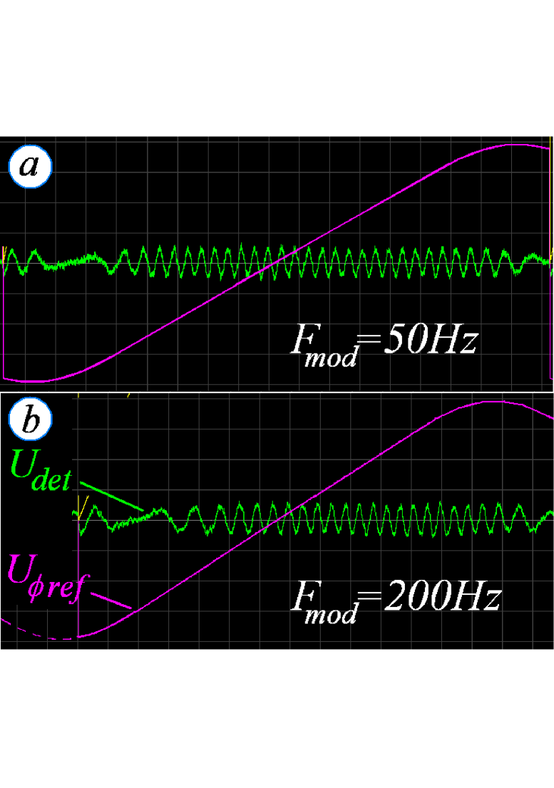
There is also an artifact found, specific for a primary math used in a system being described. If a sample contains some large light-scattering features (e.g. an edge of the sample wafer or a metal structure on a semiconductor surface), a light wave scattered by the feature back to the interferometer provides an interference with a reference beam.
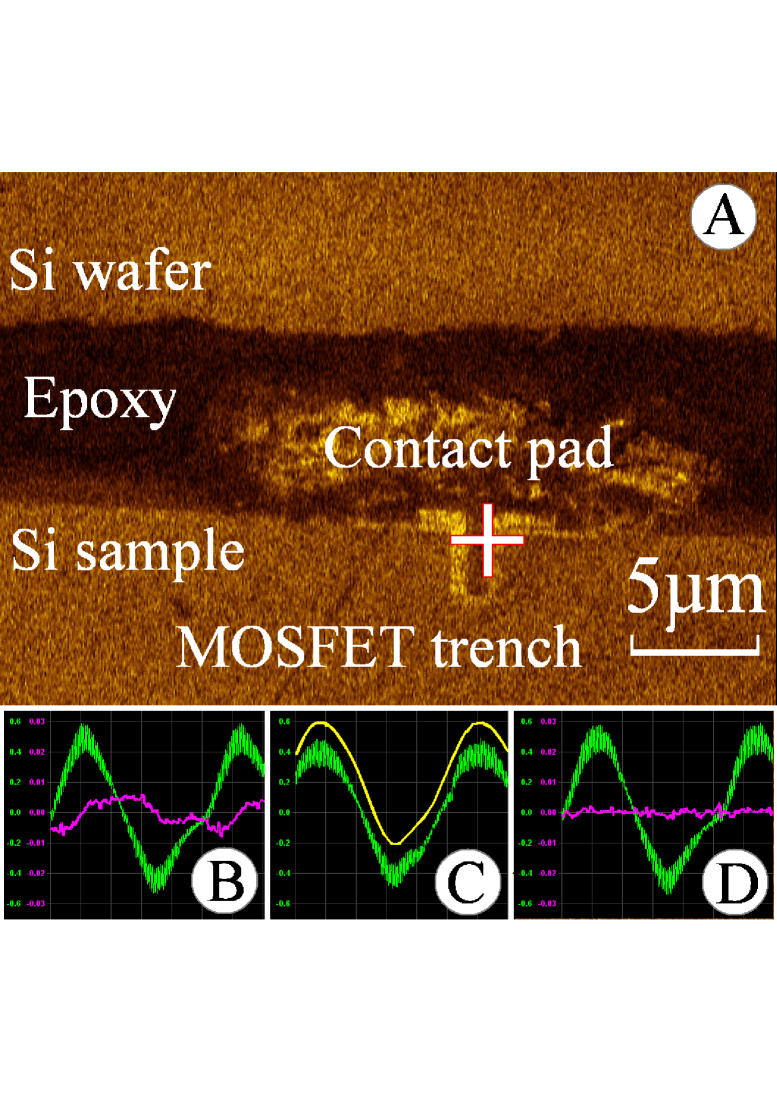
As an example, an image of the Si trench-defined MOSFET structure is present in the Fig.6. A sample was prepared in a cleaved-edge geometry. To protect the edge during polishing, a piece of dummy Si wafer was glued on a sample carrier parallel to a sample. An ASNOM signal amplitude mapped at wavelength is shown in Fig.6A. A harmonic of the tip oscillation frequency was used in the primary math to recover a near-field component. A trench structure ( surrounded with ) covered with some metal contact strip can be seen in the figure. After map was obtained, a tip was brought to a position above the trench (marked as a cross in the map) and retracted from a surface for approx. . Since a tip-surface distance is much larger than necessary for a near-field optical coupling, one should expect absolutely no near field component in the signal being observed. Instead, one can clearly see nearly sinusoidal oscillation in a second harmonic response (Fig.6B, violet curve) in an output data of the primary math.
Due to a presence of the sharp edges and significant difference in the optical properties of the materials (, , , , epoxy), the light scattered by the sample back is rather strong, and a parasite interference component is noticeable. To save a CPU time, no data apodization is applied before Fourier-processing. In this case, if a Fourier-transform is used to recover an ASNOM component in a detector signal within each tip oscillation period (higher harmonics of ), the slope and curvature of this slow interference response would be processed as well as any other input signal by the Fourier-transform math, and produce some non-zero result (see Fig.6B). The higher modulation frequency is, the stronger is the effect. Such a ”recovered signal” has no physical reason in the terms of a near-field interaction between the tip and surface, and should be considered as a math artifact. To clean this parasite component away, a smoothed curve of an input signal (see Fig.6C) should be subtracted from the detector data before a primary math. Since just a general shape of a parasite interference law is relevant for the correction, the smoothening curve is built on the basis of signal average values calculated within each period. This (relatively short, ) array of numbers is used to build a fit curve. Just a few first (3..5) harmonic components within this array are calculated to describe the curve shape. After that, these constants are used to interpolate the correction curve inside a period of the tip oscillation ( points for each period, depending on ADC sampling rate being set). To save a CPU time, Tailor series (with coefficients calculated from the data mentioned above) could be used for interpolation instead of Fourier series. Finally, a parasite component could be cleaned away completely (see Fig.6D), and this is rather important for an artifact-free ASNOM imaging of the weakly-scattering samples, which produce low useful signal.
IX Conclusions
A sensitive, flexible data acquisition and signal recovery system is developed. A modular structure of a software makes easy modify the functionality of the system. A clear subdivision of the data processing stages allows user visually control the intermediate data on a virtual oscilloscope screen and detect the misalignments in the system by the signal shape distortions being observed.
Even a modest CPU rate of 300 MHz in a data acquisition card and of 2.66 GHz (Quad-CPU) in a host computer is enough to recover an ASNOM component in a detector response without losses of data. Nevertheless, we should mention that an ADC sampling rate above 6 MSPS makes an operation less stable, so that the target card may hang in some minutes or hours. It was found also, that a DAC sampling rate above 100 kSPS may cause some troubles at a high ADC sampling rates. Nevertheless, these sampling rates are much higher than ones necessary for a successful operation. The most limiting feature in our opinion is the mirror oscillation frequency, because a single data point of an ASNOM map can be acquired just within of a mirror oscillation period. With a modulation frequency of 200 Hz it means that a single point acquisition requires 5 ms (or 2.5 ms if ascening and descending mirror travels are sent to output separately).
X Acknowledgements
The work was supported by a German National Science Foundation (DFG grant KA3105/1-1). Author thanks Dr. R.Hillenbrand, Dr. F.Keilmann and Dr. N.Ocelic for their valuable discussions concerning principles of an ASNOM signal recovery.
References
- Zenhausern, O’Boyle, and Wickramasinghe (1994) F. Zenhausern, M. P. O’Boyle, and H. K. Wickramasinghe, Applied Physics Letters 65, 1623 (1994).
- Zenhausern, Martin, and Wickramasinghe (1995) F. Zenhausern, Y. Martin, and H. K. Wickramasinghe, Science 269, 1083 (1995).
- Martin, Zenhausern, and Wickramasinghe (1996) Y. Martin, F. Zenhausern, and H. K. Wickramasinghe, Applied Physics Letters 68, 2475 (1996).
- Knoll et al. (1997) B. Knoll, F. Keilmann, A. Kramer, and R. Guckenberger, Applied Physics Letters 70, 2667 (1997).
- Hillenbrand, Knoll, and Keilmann (2001) R. Hillenbrand, B. Knoll, and F. Keilmann, Journal of Microscopy 202, 77 (2001).
- Knoll and Keilmann (1999) B. Knoll and F. Keilmann, Nature 399, 134 (1999).
- Wurtz, Bachelot, and Royer (1998) G. Wurtz, R. Bachelot, and P. Royer, Review of Scientific Instruments 69, 1735 (1998).
- Krenn et al. (1999) J. R. Krenn, A. Dereux, J. C. Weeber, E. Bourillot, Y. Lacroute, J. P. Goudonnet, G. Schider, W. Gotschy, A. Leitner, F. R. Aussenegg, and C. Girard, Phys. Rev. Lett. 82, 2590 (1999).
- Brehm et al. (2006) M. Brehm, T. Taubner, R. Hillenbrand, and F. Keilmann, Nano Letters 6, 1307 1310 (2006).
- Anderson (2000) M. S. Anderson, Applied Physics Letters 76, 3130 (2000).
- Hayazawa et al. (2002) N. Hayazawa, A. Tarun, Y. Inouye, and S. Kawata, Journal of Applied Physics 92, 6983 (2002).
- Labardi, Patanè, and Allegrini (2000) M. Labardi, S. Patanè, and M. Allegrini, Applied Physics Letters 77, 621 (2000).
- Maghelli et al. (2001) N. Maghelli, M. Labardi, S. Patanè, F. Irrera, and M. Allegrini, Journal of Microscopy 202, 84 (2001).
- Bek, Vogelgesang, and Kern (2006) A. Bek, R. Vogelgesang, and K. Kern, Review of Scientific Instruments 77, 043703 (2006).
- Ocelic, Huber, and Hillenbrand (2006) N. Ocelic, A. Huber, and R. Hillenbrand, Applied Physics Letters 89, 101124 (2006).
- Esslinger et al. (2012) M. Esslinger, J. Dorfmüller, W. Khunsin, R. Vogelgesang, and K. Kern, Review of Scientific Instruments 83, 033704 (2012).
- P (25) “http://www.innovative-dsp.com/support/manuals/p25m.pdf,” P.10.
- (18) I. I. I. P. board, “http://www.physikinstrumente.com/en/products/prspecs.php?sortnr=300600,” .
- Kazantsev and Ryssel (2013) D. V. Kazantsev and H. Ryssel, Modern Instrumentation 2, 33 (2013).
- Hillenbrand and Keilmann (2000) R. Hillenbrand and F. Keilmann, Phys. Rev. Lett. 85, 3029 (2000).
- Esteban et al. (2008) R. Esteban, R. Esteban, R. Vogelgesang, J. Dorfmüller, A. Dmitriev, C. Rockstuhl, C. Etrich, and K. Kern, Nano Letters 8, 3155 (2008).
- E- (503) P. I. G. E-503, “http://www.physikinstrumente.com/en/products/prspecs.php?sortnr=602200,” .
- S-316 (a) P. I. G. S-316, “http://www.physikinstrumente.com/en/products/prspecs.php?sortnr=300600,” (a).
- S-316 (b) P. I. G. S-316, “http://www.physikinstrumente.com/en/pdf/s310 datasheet.pdf,” (b).