Stimulated Phonon Emission in a Driven Double Quantum Dot
The compound semiconductor gallium arsenide (GaAs) provides an ultra-clean platform Jesus_Nature_mat ; Umansky for storing and manipulating quantum information, encoded in the charge or spin states of electrons confined in nanostructures Hanson:2007eg . The absence of inversion symmetry in the zinc-blende crystal structure of GaAs however, results in strong piezoelectric coupling between lattice acoustic phonons and electrons Fujisawa97 ; Brandes_Kramer , a potential hinderance for quantum computing architectures that can be charge-sensitive during certain operations Hayashi ; Petta_science05 ; Petta_PRL10 ; Yacoby2qubit ; Granger_NatPhys . Here we examine phonon generation in a GaAs double dot, configured as a single- or two-electron charge qubit, and driven by the application of microwaves via surface gates Petta_PRL04 . In a process that is a microwave analog of the Raman effect, stimulated phonon emission is shown to produce population inversion of a two-level system Dykman ; Stace_PRL05 and provides spectroscopic signatures of the phononic environment created by the nanoscale device geometry.
Devices based on GaAs are advantageous for hosting qubits because the electron’s small effective mass in this material gives rise to a large level-splitting, the lack of valley degeneracy in the band structure simplifies operation, and the clean epitaxial interface used to confine electrons leads to inherently low charge noise Jesus_Nature_mat . A potential drawback of GaAs and other group III-V compounds Nadj-Perge is the presence of nuclear spins in the host lattice which can rapidly dephase electron spin-states Hanson:2007eg . Dynamical-decoupling techniquesMJB_DJR_NV however, have recently addressed dephasing from nuclei, demonstrating Bluhm that spin coherence can be preserved for times long enough that it is now important to address additional decoherence mechanisms such as residual charge noise and processes that incoherently couple electrons to phonons, either directly phonons , or via the spin orbit interaction Stano06 ; Khaetskii00 ; Loss05 . In this respect, the piezoelectric nature of GaAs, while advantageous for shuttling electrons long distancesHermelin11 ; McNeil11 , also opens a channel for enhanced relaxation and dephasing, in particular, for qubit states with a charge dipole Petta_science05 ; Yacoby2qubit .
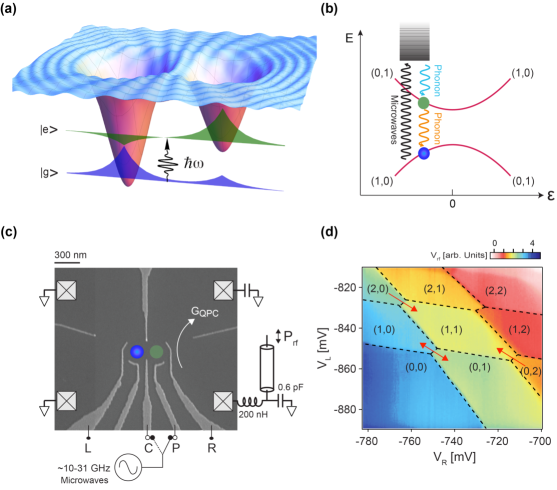
Here we investigate a phonon emission process which, because of the strong piezoelectric coupling, limits charge coherence in GaAs, even in ideal structures at zero temperature. Similar phonon generation mechanisms have recently been examined in the context of readout backaction Granger_NatPhys and compared with transport measurements of InAs nanowires double dots Weber ; Roulleau and graphene Roulleau . Our test system is a charge qubit with one or two electrons in a double quantum dot, controlled by resonant microwavesKouwenhoven_PRL94 ; Petta_PRL04 which drive Rabi oscillations of the electron between the ground and excited states, as shown schematically in Fig. 1(a). In the detuned regime where the microwave energy exceeds the qubit level splitting (see Fig. 1(b)), we show that this system undergoes stimulated phonon emission, a process which interrupts coherent driving and leads to population inversion, as predicted theoretically Dykman ; Stace_PRL05 . This mechanism, which is a microwave version of the well known optical technique of Raman spectroscopy, provides a means of detecting the phonon spectral density created by the unique nanoscale device geometry. Our experimental results are in agreement with a theoretical model based on a non-Markovian master equation and we suggest approaches to suppress the electron-phonon coupling which could further improve coherence times.


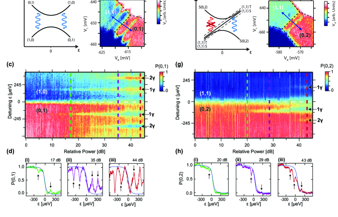
A micrograph of our double quantum dot device is shown in Fig. 1(c), including a proximal rf quantum point contactReilly:2007ig (rf-QPC) which is used as a sensor to read out the charge state of the system (see Fig. 1(d) and §Methods). Gate voltages and control the detuning of energy levels between the two dots. For 0 the ground and excited states of the qubit correspond to localising the electron mostly in the left (1,0) or right (0,1) dot respectively, (this is reversed for 0). We apply microwaves with an energy that matches the qubit splitting at a certain value of , coherently driving between ground and excited states. Under these conditions the readout signal exhibits sidebands that appear as lines in the charge stability diagram offset either side from the = 0 transition (Fig. 2b)). We measure the time-averaged probability of the electron being in the (0,1) charge configuration, calibrated such that (0,1) = 1 for and (0,1) = 0 for .
Close examination of the microwave sideband lineshape reveals that they are strongly asymmetric and distinct from the characteristic Lorentzian lineshape expected for a driven two-level system. This is seen clearly with increasing microwave power in Fig. 2(c), which shows pairs of sidebands corresponding to single- (1) and two- (2) microwave photon processes, positioned either side of the (1,0)-(0,1) transition. We note that the lineshape of all sidebands is strongly broadened, mostly on the side closest to = 0, which we refer to as the blue-detuned side, where the microwave photon energy exceeds the qubit splitting. Further, at high powers, the amplitude of the microwave sidebands exceeds the saturation value of (0,1) = 0.5 expected for a driven two-level system undergoing Rabi cycles between the ground and excited state. This population inversion results from Raman process in which the microwave energy exceeds the qubit level splitting, accessing the excited state by the stimulated emission of phonons at a rate that exceeds the rate of spontaneous decay Dykman ; Stace_PRL05 (see Fig. 1(b)).
Our device can also be configured to the (2,0)-(1,1) charge transition by adjusting the gate potential to allow two electrons to occupy the double dot (see Fig. 1(d)). Under microwave excitation we again observe sidebands that are strongly asymmetric in their lineshape. A key difference in the two-electron case however, is the presence of Pauli-blockade Johnson_PRB05 which leads to spin dependent transitions when driving resonantly with microwaves Schreiber . This behaviour is evident in Fig. 2(e-h) as a strong suppression in the sideband amplitude on the (1,1) side of the transition, where 0. We attribute this suppression to the occupation of a triplet state which cannot tunnel to the (0,2) singlet state under microwave excitation without a spin flip. The maximum height of the suppressed sideband in (1,1) is set by the ratio of singlets to triplets, (1:3 (0.25 (0,2) = 0.5), gives = 0.125). We find this spin-dependent suppression is unchanged for magnetic fields in the range = 0 – 4 T foot1 .
Even in the limit of weak microwave driving, where the system does not exhibit population inversion, stimulated emission of phonons will lead to decoherence of charge states in GaAs devices. The probability for stimulated emission is weighted by the density of available phonon modes subject to the boundary conditions of the nanoscale device geometry. In an effort to uncover this geometric fingerprint in the lineshape, we make use of the high bandwidth of the rf-QPC charge detector to rapidly average over many data sets so that the sidebands can be observed with high resolution, as shown in Fig. 3(a-d) for a range of microwave powers in the weak driving regime. Comparing the averaged data to the Lorentzian lineshape expected for a weakly driven qubit in the Markovian regime StaceBarrett (solid line), it is evident that the blue-detuned region of the sideband shows fine, step-like features Stace_PRL05 in the excited state probability (0,1) as a function of detuning. On the ‘red’ side, the data also deviates slightly from the Lorentzian form and exhibits additional structure. Via comparison to a detailed theoretical model Stace_new , we identify these aspects as signatures of the strong coupling between the driven qubit and its phononic environment.
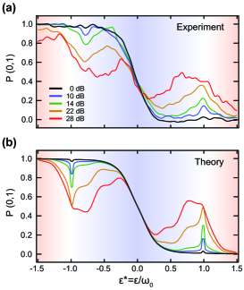
Our model describes the driven system with a master equation, allowing the Rabi frequency to be comparable to the decay rate. In order to incorporate Raman processes in the weak driving limit our model does not make the usual assumption of Markovian dynamics StaceBarrett ; Stace_PRL05 . Taking the Laplace transform of the von Neumann equation gives a series of expressions that describe the dynamical steady state, dependent on the detuning , the inter-dot tunnelling rate , the electric field-dipole Rabi frequency , the microwave driving frequency , the temperature , and the spectral density, , where is the device geometry dependent electron-phonon coupling amplitude, is the phonon frequency and is the transition frequency. Figure 4 compares experimental data with our theoretical model using the materials properties of GaAs (see §Methods for details). The only free parameter of this microscopic model is the global scaling of the microwave amplitude. The colour of the traces indicates the microwave driving amplitudes with values consistent between experiment (a) and theory (b).
With this model in hand we comment further on several features that are evident in the experimental data and accounted for by the theory. Firstly, the step features appearing on the blue side of each sideband are understood in terms of a Raman transition involving the simultaneous absorption of a photon and emission of a phonon, weighted by the phonon spectral density and set by the device geometry. The width of each step (see Fig. 3) is directly related to the spacing between the quantum dots and can be considered as a double-slit interference pattern for emitting a phonon on the left or right dots during microwave drive. A shoulder to the lineshape on the red-side of the sideband is also evident and arises from a renormalisation of the qubit detuning and Rabi frequency when the bare electron interacts with the phononic environment of the crystal lattice. This renormalisation of the detuning is analogous to the Lamb-shift, and arises in Markovian models, whilst the renormalised Rabi frequency only appears when accounting for the dynamical steady-state of the driven system.
There are also some discrepancies between our model and the experimental data. These can likely be explained by the anisotropy of the piezoelectric coupling, which we have neglected in the model. Further, we have not considered the presence of the surface which modifies the phononic spectral density. For the present device, where the double dots are located 110 nm below the surface, constructive interference between the double-dot dipole and its image charge couple the electrons to Rayleigh surface acoustic waves. We note that the ability to control the crystallographic orientation of the double dot and its depth from the surface offers a means of suppressing electron-phonon coupling, an advantage of heterostructure devices. Future approaches to suppressing the influence of the phononic environment may include patterning the surface or shaping the gate electrodes to induce phononic band gaps Painter that extend qubit coherence in these systems.
I Methods
The double dot is defined electrostatically, 110 nm below the surface of a GaAs/Al0.3Ga0.7As heterostructure grown using molecular beam epitaxy (electron density 2.4 10 15 m -2, mobility 44 m 2/Vs at 20 K). All data is taken at the base electron temperature of a dilution refrigerator, 100 mK, with the sample mounted on a custom high frequency printed circuit board (PCB) CollessRSI . Microwave excitation is produced using a room temperature vector source (Agilent 8267D) and fed to the device PCB via coaxial cables that include cryogenic attenuators.
Readout is performed using an rf quantum point contact (rf-QPC), proximal to the double dot. An impedance matching tank circuit operating at a frequency of 500 MHz transforms the high QPC resistance towards the 50 characteristic impedance of a transmission line enabling the QPC to modulate the amount of reflected rf power. The change in reflected rf power is amplified using cryogenic and room temperature amplifiers and demodulated at room temperature using standard quadrature mixing techniques to yield a baseband signal proportional to the QPC conductance. For high resolution data (Figure 3 and Figure 4) a high bandwidth digital storage scope is used to perform a large number of trace averages.
To compare our theoretical model to the experimental data, we normalise each quantity with respect to the microwave driving frequency, e.g., , where the ∗ indicates dimensionless parameters. In this form we can write:
| (1) |
where , with the inter-dot separation and is the transverse speed of sound. where is the piezoelectric electron-phonon coupling strength, is the mass density, and is a high-frequency cut-off determined by the exponential decay length of the localised electronic wavefunction, . For GaAs, m/s, eV/nm and , so . For the driving frequency GHz pertinent to Fig. 4(a), and assuming nm (set by device geometry) we find . The tunnelling rate , and temperature are obtained independently from experimental data. We choose , consistent with nm.
Corresponding author, email: david.reilly@sydney.edu.au
These authors contributed equally to this work.
II Acknowledgements
We acknowledge funding from the U.S. Intelligence Advanced Research Projects Activity (IARPA), through the U.S. Army Research Office and the Australian Research Council Centre of Excellence Scheme (Grant No. EQuS CE110001013).
References
- (1) del Alamo, J. A. Nanometre-scale electronics with III-V compound semiconductors. Nature 479, 317–323 (2011).
- (2) Umansky, V. et al. MBE growth of ultra-low disorder 2DEG with mobility exceeding cm2/V s. J. Crystal Growth 311, 1658–1661 (2009).
- (3) Hanson, R., Petta, J. R., Tarucha, S. & Vandersypen, L. M. K. Spins in few-electron quantum dots. Rev. Mod. Phys. 79, 1217–1265 (2007).
- (4) Fujisawa, T. et al. Spontaneous emission spectrum in double quantum dot devices. Science 282, 932–935 (1998).
- (5) Brandes, T. & Kramer, B. Spontaneous emission of phonons by coupled quantum dots. Phys. Rev. Lett. 83, 3021–3024 (1999).
- (6) Hayashi, T., Fujisawa, T., Cheong, H., Jeong, Y. H. & Hirayama, Y. Coherent manipulation of electronic states in a double quantum dot. Phys. Rev. Lett. 91, 226804 (2003).
- (7) Petta, J. R. et al. Coherent manipulation of coupled electron spins in semiconductor quantum dots. Science 309, 2180–2184 (2005).
- (8) Petersson, K. D., Petta, J. R., Lu, H. & Gossard, A. C. Quantum coherence in a one-electron semiconductor charge qubit. Phys. Rev. Lett. 105, 246804 (2010).
- (9) Shulman, M. D. et al. Demonstration of entanglement of electrostatically coupled single-triplet qubits. Science 336, 202–205 (2012).
- (10) Granger, G. et al. Quantum interference and phonon-mediated back-action in lateral quantum-dot circuits. Nature Phys. 8, 522–527 (2012).
- (11) Petta, J. R., Johnson, A. C., Marcus, C. M., Hanson, M. P. & Gossard, A. C. Manipulation of a single charge in a double quantum dot. Phys. Rev. Lett 93, 186802 (2004).
- (12) Dykman, M. I. Relaxation of impurities in a nonresonant field and phonon amplification. Sov. J. Low Temp. Phys. 5, 89–95 (1979).
- (13) Stace, T. M., Barrett, S. D. & Doherty, A. C. Population inversion of a driven two-level system in a structureless bath. Phys. Rev. Lett. 95, 106801 (2005).
- (14) Nadj-Perge, S., Frolov, S. M., Bakkers, E. P. A. M. & Kouwenhoven, L. P. Spin-orbit qubit in a semiconductor nanowire. Nature 468, 1084–1087 (2010).
- (15) Biercuk, M. J. & Reilly, D. J. Solid-state spins survive. Nature Nanotechnology 6, 9 (2011).
- (16) Bluhm, H. et al. Dephasing time of gaas electron-spin qubits coupled to a nuclear bath exceeding 200 us. Nature Phys. 7, 109–113 (2010).
- (17) Fedichkin, L. & Fedorov, A. Decoherence rate of a semiconductor charge quit coupled to acoustic phonon reservoir. Phys. Rev. A. 69, 032311 (2004).
- (18) Stano, P. & Fabian, J. Theory of phonon-induced spin relaxation in laterally coupled quantum dots. Phys. Rev. Lett. 96, 186602 (2006).
- (19) Khaetskii, A. V. & Nazarov, Y. V. Spin relaxation in semiconductor quantum dots. Phys. Rev. B 61, 12639 (2000).
- (20) Bulaev, D. V. & Loss, D. Spin relaxation and anticrossing in quantum dots: Rashba versus dresselhaus spin-orbit coupling. Phys. Rev. B 71, 205324 (2005).
- (21) Hermelin, S. et al. Electrons surfing on a sound wave as a platform for quantum optics with flying electrons. Nature 477, 435–438 (2011).
- (22) McNeil, R. P. G. et al. On-demand single-electron transfer between distant quantum dots. Nature 477, 439–442 (2011).
- (23) Weber, C. et al. Probing Confined Phonon Modes by Transport through a Nanowire Double Quantum Dot. Phys. Rev. Lett. 104, 036801 (2010).
- (24) Roulleau, P. et al. Coherent electron-phonon coupling in tailored quantum systems. Nature Com. 2, 239 (2011).
- (25) Kouwenhoven, L. P. et al. Observation of photon-assisted tunnelling through a quantum dot. Phys. Rev. Lett 73, 3443–2446 (1994).
- (26) Reilly, D. J., Marcus, C. M., Hanson, M. P. & Gossard, A. C. Fast single-charge sensing with a rf quantum point contact. App. Phys. Lett. 91, 162101 (2007).
- (27) Johnson, A. C. et al. Singlet-triplet spin blockade and charge sensing in a few-electron double quantum dot. Phys. Rev. B. 72, 165308 (2005).
- (28) Schreiber, L. R. et al. Coupling artificial molecular spin states by photon-assisted tunnelling. Nature Com. 2, 556 (2011).
- (29) This dependence is somewhat in contrast to the recent work by schreiber Schreiber where spin blockade is lifted with microwave excitation, perhaps due to the presence of a micro-magnet on the surface of their device.
- (30) Barrett, S. D. & Stace, T. Continuous measurement of a microwave-driven solid state qubit. Phys. Rev. Lett 96, 017405 (2006).
- (31) Stace, T. M., Doherty, A. C. & Reilly, D. J. In review.
- (32) Alegre, T. P. M., Safavi-Naeini, A., Winger, M. & Painter, O. Quasi-two-dimensional optomechanical crystals with a complete phononic bandgap. Optics Express 19, 5658 (2011).
- (33) Colless, J. I. & Reilly, D. J. Cryogenic high-frequency readout and control platform for spin qubits. Rev. Sci. Instrum. 83, 023902 (2012).