Comment on “Direct Measurement of Auger Electrons Emitted from a Semiconductor Light-Emitting Diode under Electrical Injection: Identification of the Dominant Mechanism for Efficiency Droop” [Phys. Rev. Lett. 110, 177406 (2013)]
In a recent Letter 2013Iveland_PRL , Iveland et al. presented a careful spectroscopic study of the electrons emitted from the GaN -cap (the highly Mg-doped layer between the active region and the anode contact) of a forward-biased InGaN/GaN light-emitting diode (LED). Remarkably, the authors observed at least two distinct peaks in the electron energy distribution curves (EDCs), separated by about 1.5 eV.
The lower-energy peak was attributed to photoemitted electrons excited in the band bending region (BBR, near the surface of the GaN -cap) by the light generated in the active region. (The work function at the cesiated GaN surface was estimated at 2.3 eV. No information was provided in 2013Iveland_PRL about the peak wavelength of the electroluminescence spectrum but, according to 2003Vurgaftman_JAP , the energy gap of the eight In0.18Ga0.82N quantum wells (QWs) in the active region is about 2.5 eV, and numerical solution of the Poisson–Schrödinger equation 2011Chiaria_JQE suggests an effective gap of about 2.6 eV between the fundamental levels and about 3.05 eV between the second subbands of the conduction and valence bands (CB, VB).)
The authors concluded also that the only viable explanation for the higher-energy peak observed in the EDCs was the presence, at the -cap surface, of an important population of high-energy electrons generated by Auger recombination processes in the active region and quickly thermalized at the bottom of an upper valley of the CB of GaN (labeled “L valley” in 2013Iveland_PRL ). The actual position in the Brillouin zone of this satellite valley and its energy above the bottom of the conduction band () was considered still somehow uncertain by the authors. Critically, Iveland et al. assumed that the electrons collected in this satellite valley would not undergo significant relaxation towards before reaching the BBR, so that the “L valley” would act as a source of high-energy electrons for emission into the vacuum. According to 2013Iveland_PRL , no other mechanism could explain the observed EDCs, which therefore could be considered the first experimental demostration of the role of Auger recombination as an important loss mechanism responsible for LED efficiency droop.
Auger-induced leakage of high-energy carriers from the active region 1988Chik_JAP.1 has been already suggested as a relevant effect in GaN-based LEDs 2012Deppner_PSSR , but Iveland et al. go further, affirming that the signature of Auger processes may be directly observed on the EDC after the carriers have drifted through the entire extension not only of the 40 nm-thick Al0.15Ga0.85N electron blocking layer (EBL) delimiting the active region (with a conduction band offset meV with respect to the surrounding GaN layers, assuming ), but also of the 200 nm-thick GaN -cap. The description proposed in 2013Iveland_PRL hinges on three assumptions:
-
1.
the presence of a satellite valley in the CB at an energy from compatible with the observed higher-energy peak,
-
2.
a relaxation rate from that satellite valley to slow enough to allow an important fraction of electrons to reach the BBR before decaying to the bottom of the CB,
-
3.
negligible carrier heating by the electric field in the BBR, since, although electrons may gain kinetic energy in the BBR, their total energy at the surface would remain smaller than in the bulk.
In the following we will discuss these three assumptions, and we will conclude that, according to our understanding of electronic structure and high-energy carrier transport in GaN, only the first one is probably correct. (As a consequence, we will not consider another, stronger claim made in 2013Iveland_PRL , where a combined analysis of the measured EDCs and emitted light intensity is said to demonstrate unambiguously that Auger recombination is the dominant droop mechanism.)
I Local minima in the GaN conduction band
(a)

(b)
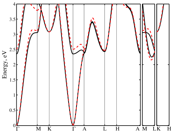
Fig. 1(a) shows the details of the CB in GaN, as computed with the nonlocal empirical pseudopotential method (NL-EPM) 2000Goano_JAP.1 ; 2007Bellotti_JAP and with density functional theory based on hybrid functionals (DFT-HSE) 2003Heyd_JCHP ; 2003Heyd_JCHP.erratum as implemented in the VASP code 1996Kresse_PRB ; 1999Kresse_PRB . (The Hartree-Fock contribution to the hybrid functional was 28%.) These results are in good agreement with each other and with state-of-the-art ab initio calculations (see e.g. 2009Delaney_APL ; 2010Svane_PRB ; 2011deCarvalho_PRB ). According to the NL-EPM bands, which will be used in the following transport analysis, the lowest secondary valley in the CB lies along the L–M segment at 2.25 eV above , while L is a saddle point, and higher local minima are at 2.35 eV () and 3.1 eV (K) above the CB minimum. The NL-EPM density of states (DOS) of the CB is reported in Fig. 1(b), where the peaks corresponding to the satellite valleys are clearly visible.
II Hot electron transport in GaN

We investigated hot electron transport in the GaN -cap of the LED studied in 2013Iveland_PRL using a full-band Monte Carlo (FBMC) simulator 2009Bertazzi_JAP that incorporates the full details of the NL-EPM bands reported above. Unlike conventional “many-valley” Monte Carlo descriptions of carrier tranport 2001Farahmand_TED ; 2012Guetle_SST ; 2013Hadi_JAP , whose results are determined by several poorly known empirical parameters (effective mass tensors and nonparabolicity coefficients for each satellite valley, intervally phonon energies and deformation potentials), FBMC does not rely on local approximations of the band structure and of the lattice dynamics, and provides a unified treatment of both intra- and inter-valley scattering processes. In particular, nonpolar carrier-phonon interactions are computed within the framework of the rigid pseudoion approximation, where the phonon dispersion relation is determined with ab initio techniques. Band-to-band tunneling effects are also included in the framework of the formalism proposed by Krieger and Iafrate 1986Krieger_PRB ; 2001Nilsson_JAP 111FBMC accurately predicts the multiplication gain and noise properties of GaN-based avalanche photodiodes (APDs) 2009Moresco_JAP and nonstationary transport effects observed by time-resolved electroabsorption measurements 2003Wraback_APL ..
Transport through the GaN -cap of hot electrons due to Auger recombination processes in the active region was studied by simulating the injection, immediately above the heterointerface between EBL and -cap, of electrons with energies higher than the satellite valleys of the GaN CB (L–M, , K) and with wave vectors randomly distributed in the whole Brillouin zone, as expected if Auger recombination is phonon-assisted.
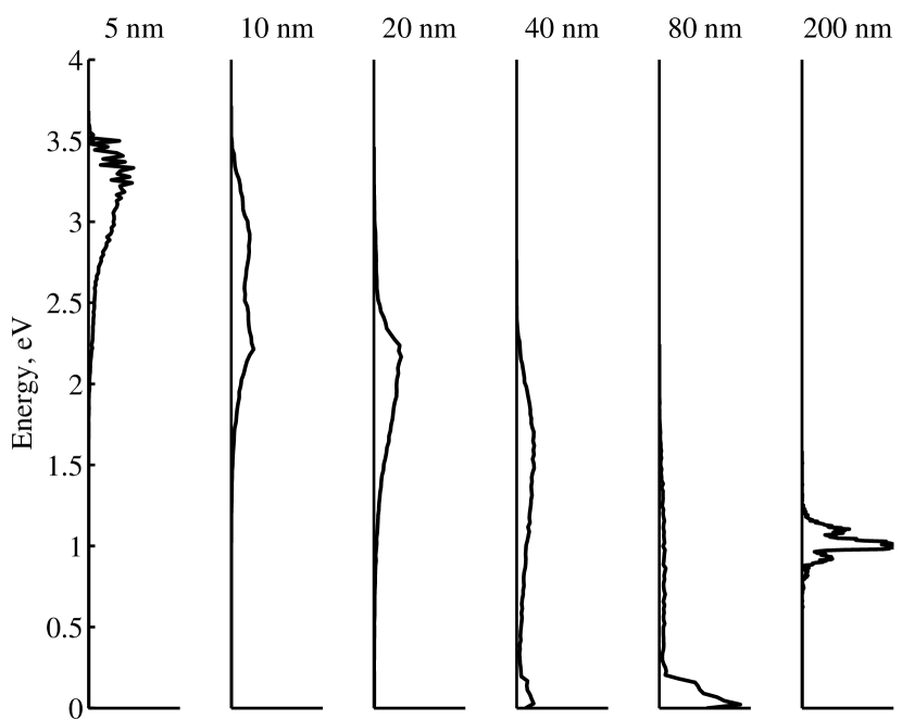
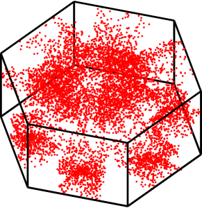
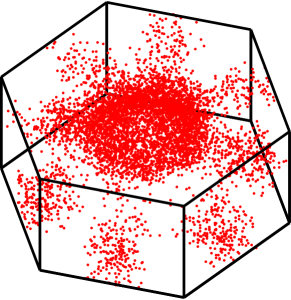
Fig. 2 reports the simulated EDCs in the GaN -cap at increasing distance from the interface with the EBL. The corresponding electron distributions in the Brillouin zone are shown in Fig. 3. It may be observed that hot electrons thermalize in the valley at the bottom of the CB (i.e. at energies much smaller than the observed higher-energy peak) in less than half the -cap thickness before reaching the BBR.
The FBMC results presented in Fig. 2 are probably conservative, because they neglect (1) carrier thermalization in the nm thick EBL and (2) carrier-carrier scattering mechanisms, which would further accelerate the relaxation process 1991Mosko_PRB .
These results suggest that the higher-energy peaks in the measured EDCs are probably uncorrelated with the carrier distribution in the active region. This would not imply that Auger recombination, and possibily Auger-induced leakage 2012Deppner_PSSR , play a negligible role in LED droop, but that an Auger signature cannot be recovered from the experiment presented in 2013Iveland_PRL if our understanding of the LED structure under investigation is correct.
III Carrier heating by the electric field in the BBR
(a)
(b)
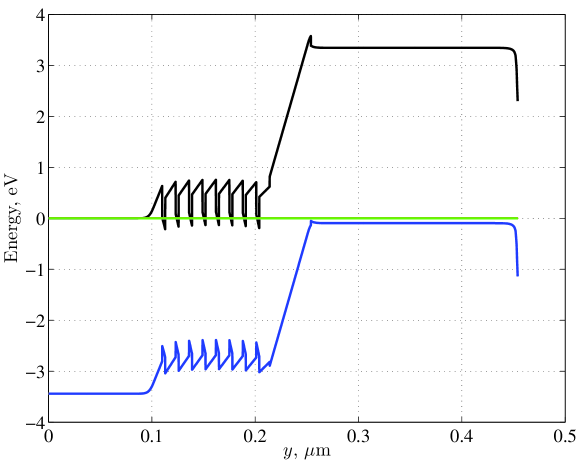
The physical mechanisms responsible for the observed bimodal EDC should be identified in order to assess whether the technique proposed in 2013Iveland_PRL can be actually used to probe the energy distribution function of carriers in the active region of an appropriately designed GaN-based LED. An explanation of the experiment would require more details about the complex device under study, in particular at the -cap surface, in order to allow a realistic two- or three-dimensional analysis, and about the Mg doping profile to assess possible surface segregation 2002Figge_APL . From the information provided in 2013Iveland_PRL , we can speculate that carrier heating by the electric field in the BBR could account for the higher-energy peak.
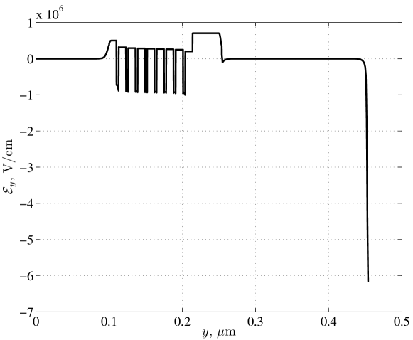
The electric field profile across the GaN -cap used in the FBMC analysis was computed with a drift-diffusion simulator (APSYS from Crosslight Software Inc.) taking into account incomplete dopant ionization 2011Chiaria_JQE and assuming a conservative band bending of about 1 eV at the cesiated surface 1999Wu_JAP ; 2004Liu_APL in accordance with the work function eV determined in 2013Iveland_PRL . With an Mg density in the -cap cm-3, as estimated in 2013Iveland_PRL , and an acceptor ionization energy meV, the calculated BBR has an extension of about 10 nm (comparable with the mean free path in GaN) and the vertical component of the electric field has a peak value of about 6 MV/cm at the -cap surface (see Fig. 4). Both values are largely independent from the applied bias, since they are essentially determined by the complete ionization of the Mg impurities near the -cap surface because of the cesiation-induced band bending.
Thermalized electrons approaching the BBR are accelerated by the large electric field and propagate quasi-ballistically to the surface. The resulting simulated EDC at the -cap surface (Fig. 2, 200 nm) exhibits a single peak lying at a kinetic energy corresponding to the total band bending. The energy of this peak is unrelated with the energy of the satellite valleys in the CB (according to the FBMC simulation, all electrons in the BBR are still in the valley). (Very similar EDCs, not reported here, were observed also when considering in the simulations, with the same band bending at the cesiated surface, lower Mg densities in the -cap down to , corresponding to electric field peaks always in the MV/cm range.)
If this description is correct 222As an additional speculation, the higher-energy peak in the EDC was not observed in 2013Iveland_PRL under external optical excitation at energy close to the LED emission possibly because electron photoemission does not occur, as suggested by Iveland et al., in the GaN BBR (which is almost transparent to the electroluminescence in the active region and is depleted of both electrons and holes if the LED is not above threshold) but only in the Cs activation layer, where it would originate the measured lower-energy peak., the higher-energy peak observed in the experimental EDCs could be ascribed to electrons reaching the BBR after escaping from the active region either because of Auger-induced leakage, or through other leakage/flyover mechanisms 2012Saguatti_TED ; e.g., APSYS simulations suggest that thermionic leakage could be significant in the LED under test even in the presence of relevant Auger recombination.
Acknowledgements.
The authors would like to thank Prof. Bernd Witzigmann, Dr. Matteo Meneghini, Michel Lestrade and Marco Vallone for useful discussions.References
- (1) J. Iveland, L. Martinelli, J. Peretti, J. S. Speck, and C. Weisbuch, “Direct measurement of Auger electrons emitted from a semiconductor light-emitting diode under electrical injection: Identification of the dominant mechanism for efficiency droop,” Phys. Rev. Lett., vol. 110, p. 177406, Apr. 2013.
- (2) I. Vurgaftman and J. R. Meyer, “Band parameters for nitrogen-containing semiconductors,” J. Appl. Phys., vol. 94, no. 6, pp. 3675–3696, Sept. 2003.
- (3) S. Chiaria, M. Goano, and E. Bellotti, “Numerical study of ZnO-based LEDs,” IEEE J. Quantum Electron., vol. 47, no. 5, pp. 661–671, May 2011.
- (4) K. D. Chik, “A theoretical analysis of Auger recombination induced energetic carrier leakage in GaInAsP/InP double heterojunction lasers and light emitting diodes,” J. Appl. Phys., vol. 63, no. 9, pp. 4688–4698, 1988.
- (5) M. Deppner, F. Römer, and B. Witzigmann, “Auger carrier leakage in III-nitride quantum-well light emitting diodes,” Phys. Stat. Sol. RRL, vol. 6, no. 11, pp. 418–420, 2012.
- (6) M. Goano, E. Bellotti, E. Ghillino, G. Ghione, and K. F. Brennan, “Band structure nonlocal pseudopotential calculation of the III-nitride wurtzite phase materials system. Part I. Binary compounds GaN, AlN, and InN,” J. Appl. Phys., vol. 88, no. 11, pp. 6467–6475, Dec. 2000.
- (7) E. Bellotti, F. Bertazzi, and M. Goano, “Alloy scattering in AlGaN and InGaN: A numerical study,” J. Appl. Phys., vol. 101, no. 12, p. 123706, 2007.
- (8) J. Heyd, G. E. Scuseria, and M. Ernzerhof, “Hybrid functionals based on a screened coulomb potential,” J. Chem. Phys., vol. 118, no. 18, pp. 8207–8215, 2003.
- (9) ——, “Erratum: Hybrid functionals based on a screened coulomb potential” [j. chem. phys. [bold 118], 8207 (2003)],” J. Chem. Phys., vol. 124, no. 21, p. 219906, 2006.
- (10) G. Kresse and J. Furthmüller, “Efficient iterative schemes for ab initio total-energy calculations using a plane-wave basis set,” Phys. Rev. B, vol. 54, pp. 11 169–11 186, Oct. 1996.
- (11) G. Kresse and D. Joubert, “From ultrasoft pseudopotentials to the projector augmented-wave method,” Phys. Rev. B, vol. 59, no. 3, pp. 1758–1775, Jan. 1999.
- (12) K. T. Delaney, P. Rinke, and C. G. Van de Walle, “Auger recombination rates in nitrides from first principles,” Appl. Phys. Lett., vol. 94, p. 191109, 2009.
- (13) A. Svane, N. E. Christensen, I. Gorczyca, M. van Schilfgaarde, A. N. Chantis, and T. Kotani, “Quasiparticle self-consistent GW theory of III-V nitride semiconductors: Bands, gap bowing, and effective masses,” Phys. Rev. B, vol. 82, p. 115102, Sept. 2010.
- (14) L. C. de Carvalho, A. Schleife, and F. Bechstedt, “Influence of exchange and correlation on structural and electronic properties of AlN, GaN, and InN polytypes,” Phys. Rev. B, vol. 84, p. 195105, Nov. 2011.
- (15) F. Bertazzi, M. Moresco, and E. Bellotti, “Theory of high field carrier transport and impact ionization in wurtzite GaN. Part I: A full band Monte Carlo model,” J. Appl. Phys., vol. 106, no. 6, p. 063718, Sept. 2009.
- (16) M. Farahmand, C. Garetto, E. Bellotti, K. F. Brennan, M. Goano, E. Ghillino, G. Ghione, J. D. Albrecht, and P. P. Ruden, “Monte Carlo simulation of electron transport in the III-nitride wurtzite phase materials system: Binaries and ternaries,” IEEE Trans. Electron Devices, vol. ED-48, no. 3, pp. 535–542, Mar. 2001.
- (17) F. Gütle, V. M. Polyakov, M. Baeumler, F. Benkhelifa, S. Müller, M. Dammann, M. Cäsar, R. Quay, M. Mikulla, J. Wagner, and O. Ambacher, “Radiative inter-valley transitions as a dominant emission mechanism in AlGaN/GaN high electron mobility transistors,” Semiconductor Sci. Tech., vol. 27, no. 12, p. 125003, 2012.
- (18) W. A. Hadi, P. K. Guram, M. S. Shur, and S. K. O’Leary, “Steady-state and transient electron transport within wurtzite and zinc-blende indium nitride,” J. Appl. Phys., vol. 113, no. 11, p. 113709, 2013.
- (19) J. B. Krieger and G. J. Iafrate, “Time evolution of Bloch electrons in a homogeneous electric field,” Phys. Rev. B, vol. 33, no. 8, pp. 5494–5500, Apr. 1986.
- (20) H.-E. Nilsson, A. Martinez, E. Ghillino, U. Sannemo, E. Bellotti, and M. Goano, “Numerical modeling of hole interband tunneling in wurtzite GaN and SiC,” J. Appl. Phys., vol. 90, no. 6, pp. 2847–2852, Sept. 2001.
- (21) FBMC accurately predicts the multiplication gain and noise properties of GaN-based avalanche photodiodes (APDs) 2009Moresco_JAP and nonstationary transport effects observed by time-resolved electroabsorption measurements 2003Wraback_APL .
- (22) M. Moško and A. Mošková, “Ensemble Monte Carlo simulation of electron-electron scattering: Improvements of conventional methods,” Phys. Rev. B, vol. 44, no. 19, pp. 10 794–10 803, Nov. 1991.
- (23) S. Figge, R. Kröger, T. Böttcher, P. L. Ryder, and D. Hommel, “Magnesium segregation and the formation of pyramidal defects in p-gan,” Appl. Phys. Lett., vol. 81, no. 25, pp. 4748–4750, 2002.
- (24) C. I. Wu and A. Kahn, “Electronic states and effective negative electron affinity at cesiated p-GaN surfaces,” J. Appl. Phys., vol. 86, no. 6, pp. 3209–3212, 1999.
- (25) Z. Liu, F. Machuca, P. Pianetta, W. E. Spicer, and R. F. W. Pease, “Electron scattering study within the depletion region of the GaN(0001) and the GaAs(100) surface,” Appl. Phys. Lett., vol. 85, no. 9, pp. 1541–1543, 2004.
- (26) As an additional speculation, the higher-energy peak in the EDC was not observed in 2013Iveland_PRL under external optical excitation at energy close to the LED emission possibly because electron photoemission does not occur, as suggested by Iveland et al., in the GaN BBR (which is almost transparent to the electroluminescence in the active region and is depleted of both electrons and holes if the LED is not above threshold) but only in the Cs activation layer, where it would originate the measured lower-energy peak.
- (27) D. Saguatti, L. Bidinelli, G. Verzellesi, M. Meneghini, G. Meneghesso, E. Zanoni, R. Butendeich, and B. Hahn, “Investigation of efficiency-droop mechanisms in multi-quantum-well InGaN/GaN blue light-emitting diodes,” IEEE Trans. Electron Devices, vol. 59, no. 5, pp. 1402–1409, May 2012.
- (28) M. Moresco, F. Bertazzi, and E. Bellotti, “Theory of high field carrier transport and impact ionization in wurtzite GaN. Part II: Application to avalanche photodetectors,” J. Appl. Phys., vol. 106, no. 6, p. 063719, Sept. 2009.
- (29) M. Wraback, H. Shen, S. Rudin, E. Bellotti, M. Goano, J. C. Carrano, C. J. Collins, J. C. Campbell, and R. D. Dupuis, “Direction-dependent band nonparabolicity effects on high-field electron transport in GaN,” Appl. Phys. Lett., vol. 82, no. 21, pp. 3674–3676, May 2003.