A System for Trapping Barium Ions in a Microfabricated Surface Trap
Abstract
We have developed a vacuum chamber and control system for rapid testing of microfabricated surface ion traps. Our system is modular in design and is based on an in-vacuum printed circuit board with integrated filters. We have used this system to successfully trap and cool barium ions and have achieved ion ‘dark’ lifetimes of with controlled shuttling of ions. We provide a detailed description of the ion trap system including the in-vacuum materials used, control electronics and neutral atom source. We discuss the challenges presented in achieving a system which can work reliably over two years of operations in which the trap under test was changed at least 10 times.
pacs:
37.10.Ty, 37.10.Rs, 32.80.Fb, 03.67.LxTrapped ions are a promising candidate building block for a quantum computer. One of the most promising trap designs is the planar ion trap. Here, RF rails and DC bias electrodes are fabricated on an aluminum surface (sometimes gold coated) on silicon using semiconductor fabrication techniques Seidelin et al. (2006); Stick et al. (2005). The basic design of these traps puts an ion in a RF pseudopotential null above the chip surface. A vapor of neutral atoms flows through an aperture in the back of the chip. Photo-ionization and laser cooling is done with beams passing just above the surface. After loading ions, the position of the trapping region can be finely controlled by adjusting the DC voltages on multiple electrodes on the trap surface while moving the lasers to follow the ion. Ultimately multiple trapping regions can be defined and ion chains can be re-organized by shuttling ions to different regions.
Chips with several designs of trapping regions have been produced. These include linear traps Amini et al. (2011); Allcock et al. (2012), multiple arm ‘Y’ Amini et al. (2010); Moehring et al. (2011) and ring traps Tabakov et al. (2012). Novel features of recently fabricated chips include integrated optics for fluorescence light collection Merrill et al. (2011); Brady et al. (2011), integrated photodetectors Eltony et al. (2013), integrated light sources Kim et al. (2011) and integrated microwave waveguides Allcock et al. (2013).
Chip traps are currently fabricated by several groups around the world. We are working with devices provided by Sandia National Labs and Georgia Tech Research Institute (GTRI). Both these groups have standardized on a 100-pin architecture which gives the ability to control up to 96 DC electrodes. Generating all the necessary control voltages and connecting them through an ultra-high vacuum (UHV) interface in a reliable and low noise way is significantly more challenging than in a traditional macroscopic ion trap.
138Ba+ is an alkaline rare-earth metal isotope with nuclear spin-0. A key advantage of barium is that all important transitions for cooling and photo-ionization reside within either the visible or near-infrared spectrum, where coherent light sources are easily obtained and transmitted with optical fibers. This feature makes barium a good candidate for implementing a photonic link qubit as part of a large scale quantum computing architecture. Barium ions have been trapped in macroscopic traps of various designs since the 1980’s Neuhauser et al. (1980); Sauter et al. (1986); Steele et al. (2007); Shu et al. (2011), though trapping of barium in a chip trap has not been demonstrated before.
I Chamber Design
Traditionally building an ion trap in a vacuum system involves wire wrapping and spot welding to make electrical connections. These techniques are well known to be compatible with the UHV environment and continued to be used once chip traps were developed. However, it was soon realized that these techniques do not scale well to chip traps which might require up to 100 connections to be made. Trap assembly is made tedious and error prone. Additionally, large numbers of point to point connections can reduce optical access and impede molecular flow.
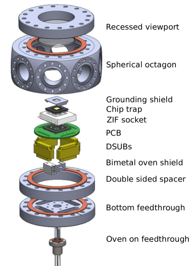
In order to facilitate easy mounting and frequent upgrades we have designed a UHV-compatible printed circuit board (PCB) that holds a custom Zero-Insertion-Force (ZIF) socket111Tactic electronics part 100-4680-001A for the chip trap. This socket accepts standard 100-pin ceramic Pin Grid Array (PGA) chip carriers used by GTRI and Sandia National Labs. These are carriers are of a square design, 33.5 mm on each side with 0.5 mm pins arranged on the outside.
The circuit board plugs in to a set of four DB-25 female/female adapters222Accu-Glass Products part 104101 which in turn are connected to feedthroughs integrated into the bottom flange333Accu-Glass Products part 25D4-133-CF600TAPPED of the vacuum chamber. A grounding shield with a window of thin wire mesh clips on to the top of the chip carrier. The circuit board incorporates 0805 series all-ceramic capacitors approximately 1 cm from the chip for filtering RF pickup on the DC control pins.
The circuit board is made of ceramic-filled Polytetrafluoroethylene (PTFE) material444Rogers ceramic (RT/duroid® 6002) of thickness with a copper cladding. It is a double sided board with plated through-holes. A particular difficulty with this material is its softness which causes it to be easily deformed by insertion pressure. In earlier iterations of the design without a ZIF socket these deformations lead to hairline cracks in the traces under the chip.
Both the ZIF socket, DB-25 adapters and a small spacer on which the ZIF socket sits555Manufactured in-house are made of Polyether Ether Ketone (PEEK). The receptacle pins for holding the ZIF socket are a gold plated brass alloy666Mill-Max part 0326-3-19-15-06-27-10-0, as are the pins which plug into the DB-25 connectors777Keystone Electronics part 1358-2. The pins for connecting the RF rails are longer888Mill-Max part 0038-3-17-15-30-27-02-0 and pass through the circuit board without connection. They are then wire-wrapped99930 AWG, silver plated copper wire with Kapton shielding to a secondary feedthrough on the vacuum chamber. All on-board connections are soldered101010Kester no-clean lead free solder (95.5% Sn, 3% Ag, 0.5% Cu) and ultrasonically cleaned with flux remover111111Chemtronics ES132 followed by acetone before assembly.
The chamber is a ‘spherical octagon’ design121212Kimbal Physics part MCF600-SphOct-F2C8. The chamber has eight 2.75 inch side ports, six of which provide optical access for the laser beams. Optical access for imaging occurs through a viewport on the top 6 inch port. Vertical space of approximately is available underneath the circuit board for mounting the atomic vapor source. Figure 1 shows an exploded view of the trap chamber.
Pumping is done with an on-system 20 L/s ion pump and a titanium sublimation pump, each connected to a 2.75 inch 5-way junction on one of the chamber ports. After baking at for 1–2 weeks we achieve a base pressure of a few Torr.
II Optical setup
The first step required in loading ions from an atomic vapor source is photo-ionization, either with a single UV source or combination of sources. Direct barium photo-ionization requires greater than photon energy (). The accumulation of UV induced charges on trap components such as Macor® parts is a known problem with wavelengths below and increases rapidly with shorter wavelengths Härter et al. (2013). The effect on PEEK and ceramic filled PTFE has not been characterized. In a chip trap surface charging is even more of a concern because the lasers must pass just 70 um above the whole surface of the chip (around 1 cm path length). Therefore we require well focused beams with small divergence and wavelength as long as practical.
In barium, the traditional approach to photo-ionization has been to use a laser to excite to the state (), followed by a UV flash from a nitrogen laser () or UV flash lamp to complete the ionization Steele et al. (2007). An alternative approaches uses a 2-photon scheme with a single laser at initially exciting the and then ionizing Rotter (2008). Another recently demonstrated alternative uses a laser to excite the strong dipole transition followed by any laser with wavelength less than to ionize Leschhorn et al. (2012).
To eliminate the use of far UV sources we use an ionization scheme in which we retain the traditional laser and employ a secondary transition, () driven with a laser131313In house design ECDL. Finally, a tertiary transition is required, the laser (or other cooling laser) can provide the necessary to complete the ionization. An additional advantage of this scheme is improved isotope selectivity.
One difficulty encountered with this scheme is that after loading we observe immediate ‘shelving’ of the ion into the state. This process can be explained by a transition via the level in the barium ion driven by incoherent light from the laser. To solve this we require a third laser for de-shelving at . This laser is obtained by frequency doubling a ECDL141414Toptica DL-Pro. The addition of this laser is not an inconvenience because it can serve as a de-shelving laser for often needed in experiments.
Primary doppler cooling is done on the transition at . This beam is derived by frequency doubling151515Custom frequency doubling crystal from HCP photonics, single fiber pigtail. a external cavity diode laser161616Toptica DL-100 (ECDL). This doubling arrangement is particularly advantageous because it allows fast switching via pickoff of a first order beam from an acousto-optic modulator (AOM) to be done in the IR. The isolation ratio when switching has traditionally been a problem in experiments. Due to the non-linearity of second-harmonic generation we achieve a very high isolation ratio which is not directly measurable. The lower limit to our isolation ratio measurement is .
A laser is also required to re-pump out of the state. This is obtained from another ECDL171717Toptica DL-100. Detecting the presence of poorly cooled ions in the initial stages of trapping is done by momentarily switching off this laser and observing a decrease in fluorescence signal.
An energy level diagram showing the relevant transitions in neutral and ionized 138Ba is shown in Figure 2. Further details of the barium doppler cooling have been presented by othersNagourney et al. (1986); Steele et al. (2007); DeVoe and Kurtsiefer (2002).
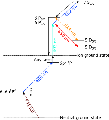
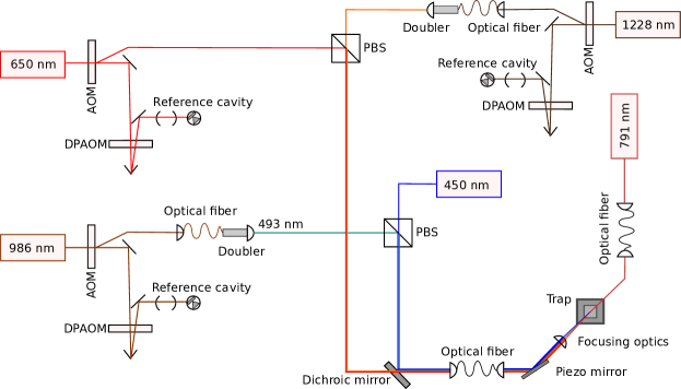
Figure 3 shows a simplified representation of the optical setup for a single beamline. The , and lasers are each frequency locked to temperature stabilized invar reference cavities in a hermetically sealed chamber using a custom top-of-the-fringe locking system. In each a zeroth-order beam from a switching AOM is passed through a double-passed AOM (DPAOM) setup to derive the beam to scan the cavity.
All of the beams except the beam reside within the transmission spectrum of Nufern 460-HP optical fiber181818Strictly is outside the transmission range but in practice can be coupled without difficulty in some fibers of this type due to manufacturing variations. and are coupled into a single optical fiber. This is particularly convenient for trapping operations because all four beams can be focused on the ion with a single setup. Coupling is achieved by first arranging combined ‘blue’ and ‘red’ beams from the + and + beams respectively each using polarizing beam splitters. These two combined beams are then further combined using a dichroic mirror191919Thor labs DMLP567 and coupled into the angle-cleaved end of an optical fiber.
The output of the fiber has a plane-cleaved end and an achromatic microscope objective is used to collimate the output beams. This is reflected by a piezo-controlled mirror202020Custom design. which allows the beam to be automatically pointed to the new ion position after shuttling. Finally a translatable lens is used for fine adjustment to focus the beams at the trapping region. Typical power levels for each of the beams at the fiber output and nominal trapping frequencies are shown in Table 1.
Efficient collection of fluorescence light from the ion is important for robust state detection. Our chamber setup makes use of a custom top mounted recessed fused silica viewport which allows imaging optics to be placed within of the trap surface. Otherwise our imaging system is conventional, employing a 20x microscope objective212121Mittitoyo M-Plan APO and second stage doublet lens.
The imaging beam path is split by a 50/50 beam splitter between a photomultiplier tube222222Hammamatsu H10682-210 (PMT) configured for photon counting and an electron-multiplying CCD camera232323Luca R series from Andor Technology. A optical bandpass filter can be switched in to the imaging beam path to block background light. Typical PMT count rates observed are counts/sec/ion against a background of counts/s. Achieving a low background count rate requires tight focusing of beams and precise leveling relative to the chip surface.
The imaging stack is mounted on a translation stage which is actuated by NEMA-23 stepper motors coupled to the micrometers via a helical coupler and brass sliding square peg coupler. This allows the imaging system to be moved automatically to image ions in different locations on the trap surface.
| Laser | Approx wavelength | Exact frequency | Power at ion |
|---|---|---|---|
| nm | THz | W | |
| Primary ionization | 791 | 250 | |
| De-shelving | 614 | 0.5 | |
| Re-pump | 650 | 50 | |
| Secondary ionization | 450 | 250 | |
| Cooling | 493 | 5 |
III Vaporization
Obtaining a beam of neutral atoms presents some unique challenges when trapping barium in a chip trap.
-
1.
Barium oxidizes readily in air and consequently the barium source must be protected from air during installation.
-
2.
The fluorescence of neutral barium atoms at is extremely weak and it has not been possible to use it to confirm the presence of neutral barium.
-
3.
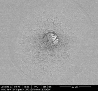
Blocking of the small loading apertures of chip traps with barium clusters can render a trap useless. Figure 4 shows a SEM image of the surface of a Sandia ring trap after testing with a traditional barium oven. This chip was also imaged with an energy-dispersive X-ray spectrograph (EDS) and the blockage identified as barium oxide.
The traditional approach to the oxidation problem has been to arrange an inert gas atmosphere and load fresh barium metal flakes into a thin alumina tube which is heated by a tungsten coil. Despite this precaution, some oxide is inevitably formed and the oven must initially run significantly hotter than usual to clean off the oxide layer. It is during this initial ‘break-in’ of a traditional oven that we expect the majority of the clusters seen in Figure 4 originate.
We have adopted a 2-part solution for reliable generation of neutral barium.
-
1.
We use a commercial barium oven242424Manufactured by Alvatec Alkali Vacuum Technologies GmbH in which the barium is contained in a stainless-steel tube filled with argon and sealed with indium. The indium seal breaks when the oven is heated. In operation the oven is heated by running current of up to through the tube. A small current (typically ) is run through the oven during the bake-out of the chamber.
-
2.
An oven shutter has been developed. This consists of a thermostatic bimetal strip252525Shivalik Bimetals type 721-112. Metals are 74-24-1 Alloy and Invar 155 Alloy. cut into an elongated ‘U’ shape with a stainless steel shutter attached. This is mounted to a Macor® block and mounted above the oven. When activated by running current through the strip it bends and moves the shutter to cover the oven tube. This protects the chip from excess barium flux and any indium from the seal. This is activated when the oven is run initially and continuously during chamber bake-out.
IV Electrical setup
Because of the large number of DC electrodes which must be controlled, using off-the-shelf equipment quickly becomes cumbersome and expensive.
We have designed a custom electrode control system. It is based on three AD5372Analog Devices Inc (2013) digital to analog converters (DACs) and controlled by a Cyclone II 2C35 field-programmable gate array (FPGA)Altera Corporation (2013). A block diagram of the system is shown in Figure 5. Electrode control solutions for shuttling ions about the chip are supplied by the manufacturer and are typically calibrated for a calcium ion with voltages in the range of . A control program running on the host PC parses the files and applies a chip and ion-species specific mapping to determine the voltages and corresponding DAC channels. The full sequence of bytes required to control the DACs is then calculated and transmitted via UDP262626User Datagram Protocol over an ethernet connection to the DAC system. The FPGA reads the data via a DM9000A ethernet interface and saves it to SRAM. Upon receipt of a control signal, the FPGA will then write the data in sequence to the three DACs.
This system has proven quite capable, allowing us to control 96 electrodes over a range (V) to within at an update rate of per channel with the ability to synchronize channel updates. Though rated for a load, internal DAC output amplifiers are sufficient to drive the in-vacuum electronics at these speeds. The final update rate depends on the number of channels that need to be updated per step; this is typically around 5–10. The system is also low cost (around $500) and compact. Source code (python control program and Verilog FPGA code) and schematics are available to other researchers on request.
The application of radio frequency (RF) to the trap is conventional. We use a copper can helical resonator to filter and impedance match from a power amplifier to the RF rails of the trap. The internal RF wires are shielded and take the shortest route possible from the feed-through to the trap. The design of helical resonators for this purpose has been explored by Siverns et.al. Siverns et al. (2012).

V Trap performance
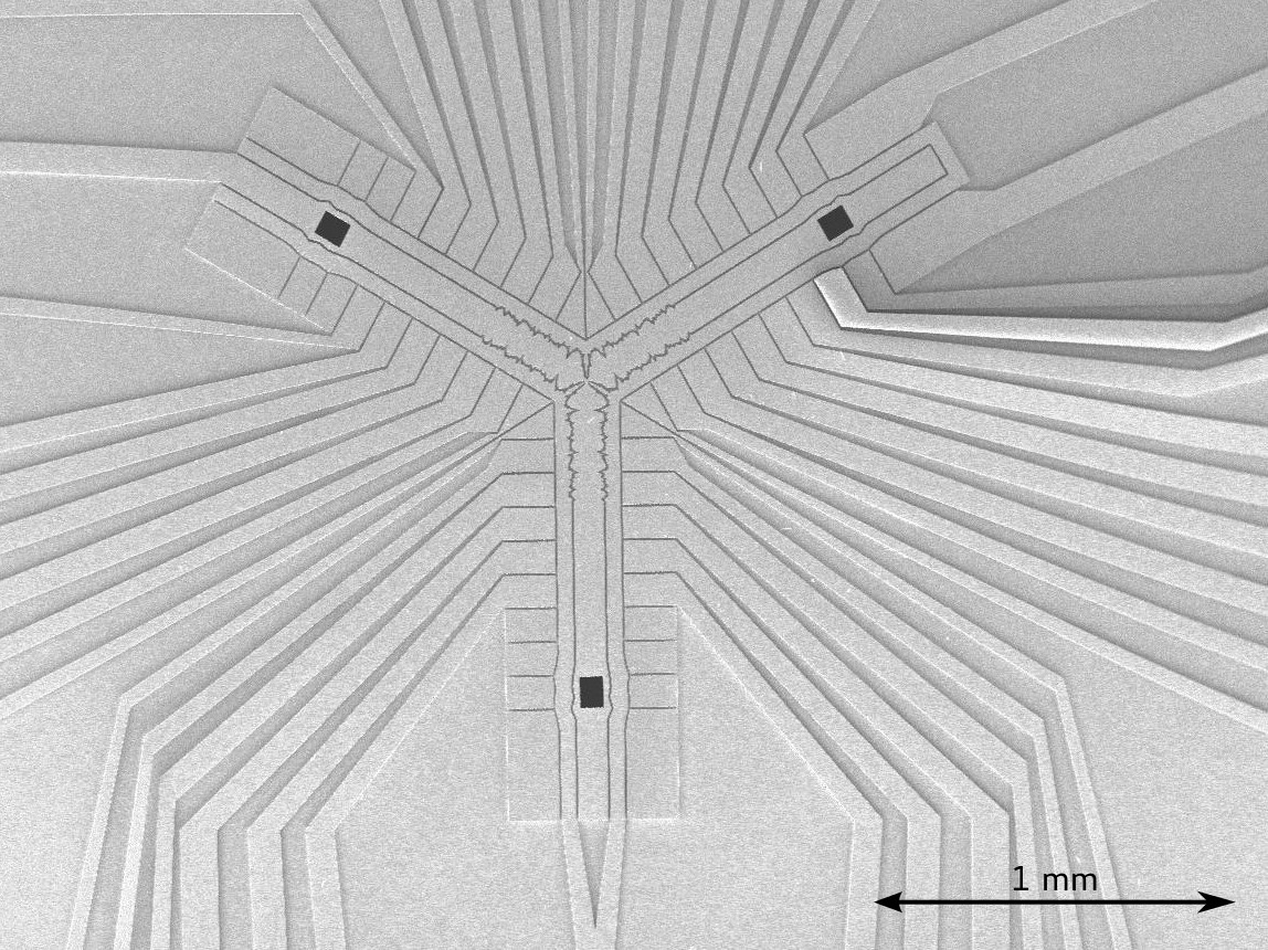
We have demonstrated trapping of single ions in our system with a ‘Y’ trap manufactured by Sandia National Labs Moehring et al. (2011). A SEM image of the surface of this trap is shown in Figure 7.
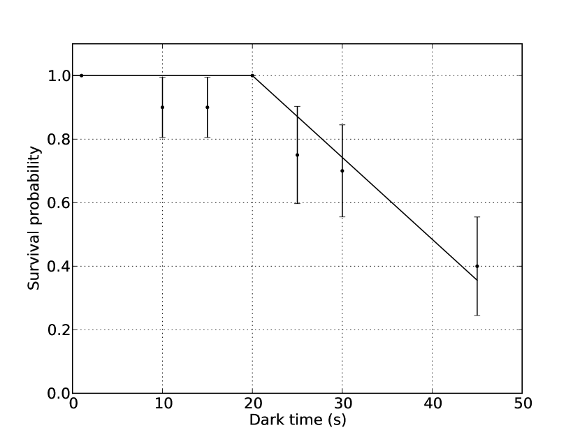
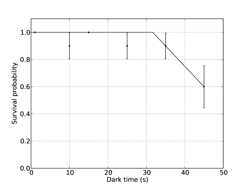
Ion dark lifetimes were measured. This was done by repeatedly mechanically shuttering the re-pump laser272727Entirely shuts off the cooling in barium. for a varying length of time and finding the probability of ion loss after cooling was re-established. Dark lifetimes have not been defined in a consistent way in the literature. In practice we are mostly interested in a measurement of the delay time over which all loss mechanisms are insignificant. Therefore we define the dark lifetime by making a weighted fit of
| (1) |
as shown in Figures 6(a) and 6(b). Uncertainties for each point are , found assuming a binomial distribution where is the number of measurements and the final parameter uncertainties are found from the covariance matrix produced after fitting with the Levenburg-Marquardt algorithm.
A dark lifetime of was measured with the ion directly over the loading region. After shuttling the ion to the mid point of one of the trap arms an improved dark lifetime of was measured. Some authors prefer the lifetime corresponding to 50% ion loss, which in our approximation is simply . Our corresponding lifetime values in this formulation are more uncertain, and respectively.
The secular frequencies of the trap were measured by the resonant excitation technique Sudakov et al. (2000). These were found to be , and . Given these we were able to determine a RF voltage of . This was done using boundary element model (BEM) solutions Slusher et al. (2010) of the surface potentials of this trap 282828BEM solutions generously supplied by C.E.Ṽolin, Georgia Tech Research Institute. and the known electrode voltages. These were combined with the RF pseudo-potential calculated for a range of realistic RF voltages (around 50 — 150 V) to form secular potential solutions at each of which the secular frequencies were solved and the best match found.
The corresponding classical well depth was found by slicing the calculated potential through the weak axis at the trapping location. We find a classical well depth of . Note that this technique does not take into account the strong stray fields above the loading region or any additional stray surface fields which are typical of these aluminum surface traps. Consequently it is most useful as a representative figure and as a point of comparison between chips of similar design.
We have repeated the calculation of the well depth at regions outside of the loading region and find comparable depths; around . Therefore, we expect the significant difference in lifetime between locations is due to excess stray fields in the loading region rather than the different trap geometry.
VI Conclusion
After operating two systems of this design for nearly two years we have found them reliable and easy to assemble. Traps can be swapped out and modifications made in a few hours; a process which has been done at least 10 times. Operating pressure (around Torr) is readily achieved after a few days of baking followed by titanium sublimation pumping. Despite the unconventional design of the system we see no evidence of any associated degradation in trap performance. The signals applied to the DC electrodes are clean, owing to the isolation from the in-vacuum filters. The AD5372 based control solution provides sufficient drive to allow convenient control of the DC voltages and is suitable for setting up trapping regions and shuttling operations.
Acknowledgements.
This research is supported by Intelligence Advanced Research Projects Activity group (IARPA).We also acknowledge Rogers Corporation and Mill-Max Mfg. Corp for proving free sample materials.
References
- Seidelin et al. (2006) S. Seidelin, J. Chiaverini, R. Reichle, J. J. Bollinger, D. Leibfried, J. Britton, J. H. Wesenberg, R. B. Blakestad, R. J. Epstein, D. B. Hume, W. M. Itano, J. D. Jost, C. Langer, R. Ozeri, N. Shiga, and D. J. Wineland, Phys. Rev. Lett. 96, 253003 (2006).
- Stick et al. (2005) D. Stick, W. Hensinger, S. Olmschenk, M. Madsen, K. Schwab, and C. Monroe, Nature Physics 2, 36 (2005).
- Amini et al. (2011) J. Amini, D. Denison, C. Doret, D. Faircloth, A. Harter, H. Hayden, T. Killian, D. Landgren, T. Merrill, A. Ozakin, C. Pai, C. Shappert, R. Slusher, K. Stevens, C. Volin, and K. Wright, Poster presentation at the MQCO Program Review, Austin TX (2011).
- Allcock et al. (2012) D. Allcock, T. Harty, H. Janacek, N. Linke, C. Ballance, A. Steane, D. Lucas, R. Jarecki, S. Habermehl, M. Blain, et al., Applied Physics B: Lasers and Optics , 1 (2012).
- Amini et al. (2010) J. Amini, H. Uys, J. Wesenberg, S. Seidelin, J. Britton, J. Bollinger, D. Leibfried, C. Ospelkaus, A. VanDevender, and D. Wineland, New journal of Physics 12, 033031 (2010).
- Moehring et al. (2011) D. L. Moehring, C. Highstrete, D. Stick, K. M. Fortier, R. Haltli, C. Tigges, and M. G. Blain, New Journal of Physics 13, 075018 (2011).
- Tabakov et al. (2012) B. Tabakov, J. Sterk, F. Benito, R. Haltli, C. Tigges, D. Stick, M. Blain, and D. Moehring, Bulletin of the American Physical Society 57 (2012).
- Merrill et al. (2011) J. Merrill, C. Volin, D. Landgren, J. Amini, K. Wright, S. Doret, C. Pai, H. Hayden, T. Killian, D. Faircloth, et al., New Journal of Physics 13, 103005 (2011).
- Brady et al. (2011) G. Brady, A. Ellis, D. Moehring, D. Stick, C. Highstrete, K. Fortier, M. Blain, R. Haltli, A. Cruz-Cabrera, R. Briggs, et al., Applied Physics B: Lasers and Optics 103, 801 (2011).
- Eltony et al. (2013) A. Eltony, S. Wang, G. Akselrod, P. Herskind, and I. Chuang, Applied Physics Letters 102, 054106 (2013).
- Kim et al. (2011) T. Kim, P. Herskind, and I. Chuang, Applied Physics Letters 98, 214103 (2011).
- Allcock et al. (2013) D. Allcock, T. Harty, C. Ballance, B. Keitch, N. Linke, D. Stacey, and D. Lucas, Applied Physics Letters 102, 044103 (2013).
- Neuhauser et al. (1980) W. Neuhauser, M. Hohenstatt, P. Toschek, and H. Dehmelt, Physical Review A 22, 1137 (1980).
- Sauter et al. (1986) T. Sauter, W. Neuhauser, R. Blatt, and P. E. Toschek, Phys. Rev. Lett. 57, 1696 (1986).
- Steele et al. (2007) A. Steele, L. Churchill, P. Griffin, and M. Chapman, Physical Review A 75, 053404 (2007).
- Shu et al. (2011) G. Shu, C.-K. Chou, N. Kurz, M. R. Dietrich, and B. B. Blinov, J. Opt. Soc. Am. B 28, 2865 (2011).
- Note (1) Tactic electronics part 100-4680-001A.
- Note (2) Accu-Glass Products part 104101.
- Note (3) Accu-Glass Products part 25D4-133-CF600TAPPED.
- Note (4) Rogers ceramic (RT/duroid® 6002).
- Note (5) Manufactured in-house.
- Note (6) Mill-Max part 0326-3-19-15-06-27-10-0.
- Note (7) Keystone Electronics part 1358-2.
- Note (8) Mill-Max part 0038-3-17-15-30-27-02-0.
- Note (9) 30 AWG, silver plated copper wire with Kapton shielding.
- Note (10) Kester no-clean lead free solder (95.5% Sn, 3% Ag, 0.5% Cu).
- Note (11) Chemtronics ES132.
- Note (12) Kimbal Physics part MCF600-SphOct-F2C8.
- Härter et al. (2013) A. Härter, A. Krükow, A. Brunner, and J. Hecker Denschlag, Applied Physics B , 1 (2013).
- Rotter (2008) D. Rotter, Quantum feedback and quantum correlation measurements with a single Barium ion, Ph.D. thesis, Leopold-Franzens-Universität Innsbruck (2008).
- Leschhorn et al. (2012) G. Leschhorn, T. Hasegawa, and T. Schaetz, Applied Physics B 108, 159 (2012).
- Note (13) In house design ECDL.
- Note (14) Toptica DL-Pro.
- Note (15) Custom frequency doubling crystal from HCP photonics, single fiber pigtail.
- Note (16) Toptica DL-100.
- Note (17) Toptica DL-100.
- Nagourney et al. (1986) W. Nagourney, J. Sandberg, and H. Dehmelt, Physical Review Letters 56, 2797 (1986).
- DeVoe and Kurtsiefer (2002) R. G. DeVoe and C. Kurtsiefer, Phys. Rev. A 65, 063407 (2002).
- Davidson et al. (1992) M. D. Davidson, L. C. Snoek, H. Volten, and A. Doenszelmann, Astronomy and Astrophysics 255, 457 (1992).
- Curry (2004) J. J. Curry, Journal of Physical and Chemical Reference Data 33, 725 (2004).
- Note (18) Strictly is outside the transmission range but in practice can be coupled without difficulty in some fibers of this type due to manufacturing variations.
- Note (19) Thor labs DMLP567.
- Note (20) Custom design.
- Note (21) Mittitoyo M-Plan APO.
- Note (22) Hammamatsu H10682-210.
- Note (23) Luca R series from Andor Technology.
- Note (24) Manufactured by Alvatec Alkali Vacuum Technologies GmbH.
- Note (25) Shivalik Bimetals type 721-112. Metals are 74-24-1 Alloy and Invar 155 Alloy.
- Analog Devices Inc (2013) Analog Devices Inc, “32-Channel, 16-/14-Bit, Serial Input, Voltage Output DAC AD5372/AD5373,” (2013).
- Altera Corporation (2013) Altera Corporation, “Cyclone II Device Handbook, Volume 1,” (2013).
- Note (26) User Datagram Protocol.
- Siverns et al. (2012) J. Siverns, L. Simkins, S. Weidt, and W. Hensinger, Applied Physics B 107, 921 (2012).
- Note (27) Entirely shuts off the cooling in barium.
- Sudakov et al. (2000) M. Sudakov, N. Konenkov, D. Douglas, and T. Glebova, Journal of the American Society for Mass Spectrometry 11, 10 (2000).
- Slusher et al. (2010) R. Slusher, J. Kim, A. Harter, J. Amini, D. Denison, D. Faircloth, H. Hayden, T. Killian, A. Ozakin, F. Shaikh, et al., Scalable Multiplexed Ion Trap (SMIT) Program, Tech. Rep. (Georgia Tech Research Institute Atlanta, Signature technology lab, 2010).
- Note (28) BEM solutions generously supplied by C.E.Ṽolin, Georgia Tech Research Institute.