Radio-frequency electromagnetic field and vortex penetration in multilayered superconductors

Takayuki Kubo kubotaka@post.kek.jp KEK, High Energy Accelerator Research Organization, 1-1 Oho, Tsukuba, Ibaraki 305-0801 Japan    Yoshihisa Iwashita Institute for Chemical Research, Kyoto University, Uji, Kyoto 611-0011 Japan    Takayuki Saeki KEK, High Energy Accelerator Research Organization, 1-1 Oho, Tsukuba, Ibaraki 305-0801 Japan
Abstract

A multilayered structure with a single superconductor layer and a single insulator layer formed on a bulk superconductor is studied. General formulae for the vortex-penetration field of the superconductor layer and the magnetic field on the bulk superconductor, which is shielded by the superconductor and insulator layers, are derived with a rigorous calculation of the magnetic field attenuation in the multilayered structure. The achievable peak surface field depends on the thickness and its material of the superconductor layer, the thickness of the insulator layer and material of the bulk superconductor. The calculation shows a good agreement with an experimental result. A combination of the thicknesses of superconductor and insulator layers to enhance the field limit can be given by the formulae for any given materials.

Technologies to fabricate the superconducting RF cavities made of Nb have been advanced. The maximum accelerating gradient Eaccsubscript𝐸accE_{\rm acc} of the TESLA type 1.3GHz1.3GHz1.3\,{\rm GHz} 9-cell cavities during performance tests in vertical cryostats regularly exceed 35MV/m35MVm35\,{\rm MV/m} at several laboratories. The gradient record had been increasing and recently two 9-cell cavities made from large grain Nb reached 45MV/m45MVm45\,{\rm MV/m} at DESY singer . Further high gradients, however, would not be expected because their gradients are thought to be close to the empirical limit imposed by the thermodynamic critical field 200mTsimilar-to-or-equalsabsent200mT\simeq 200\,{\rm mT} of Nb hassan . A. Gurevich suggested gurevich ; gurevichreview that a multilayered nanoscale coating on Nb cavity may push up the RF breakdown field to the level of the vortex-penetration field of the coating materials at which the Bean-Livingston surface barrier beanlivingston disappears. While some experimental studies have been conducted on the subject based on the idea tajima ; antoine , not much theoretical progress followed on it. In fact, the best parameter set for the multilayer coating model such as thicknesses of layers and choices of materials are not clear from a theoretical point of view. In this letter, the multilayered structure is carefully evaluated with a rigorous calculation on the electromagnetic field distribution to keep its self-consistency. The resultant vortex-penetration field, the best combination of parameters, and materials are described.

The multilayer coating model gurevich consists of alternating layers of superconductor layers (𝒮𝒮\mathcal{S}) and insulator layers (\mathcal{I}). The simplest configuration with a single superconductor layer and a single insulator layer is seen in Fig. 1. Each 𝒮𝒮\mathcal{S} layer is expected to withstand higher field than bulk Nb, and to shield the bulk Nb from the applied RF surface magnetic field B0subscript𝐵0B_{0}, because Bisubscript𝐵𝑖B_{i} (the RF surface field on the bulk Nb) is smaller than B0subscript𝐵0B_{0}. Then the multilayered structure is thought to withstand a higher field than the bulk Nb if B0subscript𝐵0B_{0} is smaller than the vortex-penetration fields of the top 𝒮𝒮\mathcal{S} layer and Bisubscript𝐵𝑖B_{i} is smaller than that of the bulk Nb. The vortex-penetration field of the 𝒮𝒮{\mathcal{S}} layer was given by Bv=ϕ0/4πλξsubscript𝐵𝑣subscriptitalic-ϕ04𝜋𝜆𝜉B_{v}=\phi_{0}/4\pi\lambda\xi in the original paper gurevich , where ϕ0=2.07×10¹⁵Wbsubscriptitalic-ϕ02.07superscript1015Wb\phi_{0}=2.07\times 10^{-15}\,{\rm Wb} is the flux quantum tinkham , and λ𝜆\lambda and ξ𝜉\xi are a London penetration depth and a coherence length of the material of the 𝒮𝒮{\mathcal{S}} layer, respectively. This expression, however, has the same form as the vortex-penetration field of the semi-infinite superconductor, and does not depend on any parameters on the configuration of the multilayered structure such as the 𝒮𝒮{\mathcal{S}} layer thickness or the {\mathcal{I}} layer thickness. In order to incorporate effects from the configuration of multilayered structure, we carried out rigorous caluculation on the distribution of magnetic field and Meissner current in the 𝒮𝒮{\mathcal{S}} layer.

Table 1: Parameters of the multilayered structure with a single superconductor layer and a single insulator layer formed on a bulk superconductor.
Region Material type Parameter
I Superconductor layer Coherence length: ξ1subscript𝜉1\xi_{1}, London penetration depth: λ1subscript𝜆1\lambda_{1} (ξ1much-greater-thanabsentsubscript𝜉1\gg\xi_{1}), Thickness: d𝒮subscript𝑑𝒮d_{\mathcal{S}} (ξ1much-greater-thanabsentsubscript𝜉1\gg\xi_{1})
II Insulator layer Relative permittivity: ϵrsubscriptitalic-ϵ𝑟\epsilon_{r}, Thickness: dsubscript𝑑d_{\mathcal{I}} (zero or larger than a few nm)
III Bulk superconductor London penetration depth: λ2subscript𝜆2\lambda_{2}

In order to derive the electromagnetic field in the multilayered structure, the Maxwell equations and the London equations should be solved with appropriate boundary conditions simultaneously. Contributions to the electromagnetic field distribution from the normal (unpaired) electrons of the superconductor and dielectric losses in the insulator are neglected. For simplicity, let us consider a model with a single 𝒮𝒮\mathcal{S} layer and a single \mathcal{I} layer formed on a bulk superconductor as shown in Fig. 1. Table. 1 shows the parameters for the model. dsubscript𝑑d_{\mathcal{I}} is assumed to be zero or larger than a few nmnm{\rm nm} to suppress the Josephson coupling gurevichreview . All layers are parallel to the y𝑦y-z𝑧z plane and then perpendicular to the x𝑥x-axis. The electric and magnetic fields are assumed to be parallel to the layers: 𝐄=(0,E,0)eiωt𝐄0𝐸0superscript𝑒𝑖𝜔𝑡{\bf E}=(0,E,0)e^{-i\omega t} and 𝐁=(0,0,B)eiωt𝐁00𝐵superscript𝑒𝑖𝜔𝑡{\bf B}=(0,0,B)e^{-i\omega t}, where E𝐸E and B𝐵B are amplitudes of electric and magnetic fields, and ω𝜔\omega is an angular frequency. Further we assume the materials used for the 𝒮𝒮{\mathcal{S}} layer is extreme Type II superconductor λ1ξ1much-greater-thansubscript𝜆1subscript𝜉1\lambda_{1}\gg\xi_{1}, and the 𝒮𝒮{\mathcal{S}} layer thickness is larger than the coherence length d𝒮ξ1much-greater-thansubscript𝑑𝒮subscript𝜉1d_{\mathcal{S}}\gg\xi_{1}. Note that the 𝒮𝒮{\mathcal{S}} layer of our model is not necessarily a thin film hence the discussion below can be applied to any 𝒮𝒮{\mathcal{S}} layer with arbitrary thickness d𝒮ξ1much-greater-thansubscript𝑑𝒮subscript𝜉1d_{\mathcal{S}}\gg\xi_{1}. Solving the Maxwell equations in the {\mathcal{I}} layers, and the London equations in the 𝒮𝒮{\mathcal{S}} layers and in the bulk superconductor with continuity conditions of electric and magnetic fields at boundaries ipac13kis , we find

BIsubscript𝐵I\displaystyle B_{\rm I} =\displaystyle= B0coshd𝒮xλ1+(λ2λ1+dλ1)sinhd𝒮xλ1coshd𝒮λ1+(λ2λ1+dλ1)sinhd𝒮λ1,subscript𝐵0subscript𝑑𝒮𝑥subscript𝜆1subscript𝜆2subscript𝜆1subscript𝑑subscript𝜆1subscript𝑑𝒮𝑥subscript𝜆1subscript𝑑𝒮subscript𝜆1subscript𝜆2subscript𝜆1subscript𝑑subscript𝜆1subscript𝑑𝒮subscript𝜆1\displaystyle B_{0}\frac{\cosh\frac{d_{\mathcal{S}}-x}{\lambda_{1}}+(\frac{\lambda_{2}}{\lambda_{1}}+\frac{d_{\mathcal{I}}}{\lambda_{1}})\sinh\frac{d_{\mathcal{S}}-x}{\lambda_{1}}}{\cosh\frac{d_{\mathcal{S}}}{\lambda_{1}}+(\frac{\lambda_{2}}{\lambda_{1}}+\frac{d_{\mathcal{I}}}{\lambda_{1}})\sinh\frac{d_{\mathcal{S}}}{\lambda_{1}}}\,, (1)
BIIsubscript𝐵II\displaystyle B_{\rm II} =\displaystyle= B01coshd𝒮λ1+(λ2λ1+dλ1)sinhd𝒮λ1,subscript𝐵01subscript𝑑𝒮subscript𝜆1subscript𝜆2subscript𝜆1subscript𝑑subscript𝜆1subscript𝑑𝒮subscript𝜆1\displaystyle B_{0}\frac{1}{\cosh\frac{d_{\mathcal{S}}}{\lambda_{1}}+(\frac{\lambda_{2}}{\lambda_{1}}+\frac{d_{\mathcal{I}}}{\lambda_{1}})\sinh\frac{d_{\mathcal{S}}}{\lambda_{1}}}\,, (2)
BIIIsubscript𝐵III\displaystyle B_{\rm III} =\displaystyle= B0exd𝒮dλ2coshd𝒮λ1+(λ2λ1+dλ1)sinhd𝒮λ1,subscript𝐵0superscript𝑒𝑥subscript𝑑𝒮subscript𝑑subscript𝜆2subscript𝑑𝒮subscript𝜆1subscript𝜆2subscript𝜆1subscript𝑑subscript𝜆1subscript𝑑𝒮subscript𝜆1\displaystyle B_{0}\frac{e^{-\frac{x-d_{\mathcal{S}}-d_{\mathcal{I}}}{\lambda_{2}}}}{\cosh\frac{d_{\mathcal{S}}}{\lambda_{1}}+(\frac{\lambda_{2}}{\lambda_{1}}+\frac{d_{\mathcal{I}}}{\lambda_{1}})\sinh\frac{d_{\mathcal{S}}}{\lambda_{1}}}\,, (3)

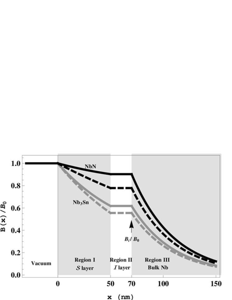
where BIsubscript𝐵IB_{\rm I}, BIIsubscript𝐵IIB_{\rm II}, and BIIIsubscript𝐵IIIB_{\rm III} are the amplitudes of magnetic fields in region I, II, and III, respectively. Note here that these equations are approximated formulae that are valid for d(ϵrk)1much-less-thansubscript𝑑superscriptsubscriptitalic-ϵ𝑟𝑘1d_{\mathcal{I}}\ll(\sqrt{\epsilon_{r}}k)^{-1}, where k=ω/c𝑘𝜔𝑐k=\omega/c, and c𝑐c is the speed of light. For example, a frequency f=ω/2π=1.3GHz𝑓𝜔2𝜋1.3GHzf=\omega/2\pi=1.3\,{\rm GHz} TDR imposes d1cmmuch-less-thansubscript𝑑1cmd_{\mathcal{I}}\ll 1\,{\rm cm} as a condition of validity. It is easy to confirm that these equations are reduced to the well known expression for the semi-infinite superconductor given by B=B0ex/λ1𝐵subscript𝐵0superscript𝑒𝑥subscript𝜆1B=B_{0}e^{-x/\lambda_{1}} when the 𝒮𝒮{\mathcal{S}} layer and the bulk superconductor are the same material (λ1=λ2subscript𝜆1subscript𝜆2\lambda_{1}=\lambda_{2}) and the {\mathcal{I}} layer vanishes (d0subscript𝑑0d_{\mathcal{I}}\to 0). Fig. 1 shows examples how a magnetic field attenuates in a multilayered structure.
Refer to caption
Figure 1: Examples of the magnetic field attenuations in the multilayered structure. Solid curves show our formulae given above, and dashed curves show the naive estimates with B=B0ex/λ1𝐵subscript𝐵0superscript𝑒𝑥subscript𝜆1B=B_{0}e^{-x/\lambda_{1}}. Black curves and gray curves correspond to the material of the 𝒮𝒮{\mathcal{S}} layer: NbNNbN{\rm NbN} (λ1=200nmsubscript𝜆1200nm\lambda_{1}=200\,{\rm nm}) and Nb3SnsubscriptNb3Sn{\rm Nb}_{3}{\rm Sn} (λ1=85nmsubscript𝜆185nm\lambda_{1}=85\,{\rm nm}), respectively. The bulk superconductor is assumed to be Nb (λ2=40nmsubscript𝜆240nm\lambda_{2}=40\,{\rm nm}). The values of λ1subscript𝜆1\lambda_{1} and λ2subscript𝜆2\lambda_{2} are given in literature gurevichreview . The thickness of the 𝒮𝒮{\mathcal{S}} layer and the {\mathcal{I}} layer are fixed at d𝒮=50nmsubscript𝑑𝒮50nmd_{\mathcal{S}}=50\,{\rm nm} and d=20nmsubscript𝑑20nmd_{\mathcal{I}}=20\,{\rm nm}.
Refer to caption
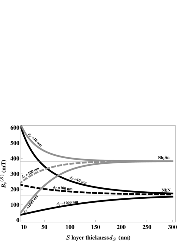
Figure 2: Vortex-penetration fields of the 𝒮𝒮{\mathcal{S}} layer, Bv(𝒮)superscriptsubscript𝐵𝑣𝒮B_{v}^{(\mathcal{S})}, as functions of an 𝒮𝒮{\mathcal{S}} layer thickness d𝒮subscript𝑑𝒮d_{\mathcal{S}}. Solid curves, dashed curves and dashed-dotted curves correspond to {\mathcal{I}} layer thickness d=10nmsubscript𝑑10nmd_{\mathcal{I}}=10\,{\rm nm}, 100nm100nm100\,{\rm nm}, and 1000nm1000nm1000\,{\rm nm}, respectively. Thin horizontal lines represents asymptotic lines, which correspond to vortex-penetration fields of thick 𝒮𝒮{\mathcal{S}} layers (d𝒮λ1much-greater-thansubscript𝑑𝒮subscript𝜆1d_{\mathcal{S}}\gg\lambda_{1}). Black curves and gray curves correspond to the material of the 𝒮𝒮{\mathcal{S}} layer: NbNNbN{\rm NbN} (λ1=200nmsubscript𝜆1200nm\lambda_{1}=200\,{\rm nm}, ξ1=5nmsubscript𝜉15nm\xi_{1}=5\,{\rm nm}) and Nb3SnsubscriptNb3Sn{\rm Nb}_{3}{\rm Sn} (λ1=85nmsubscript𝜆185nm\lambda_{1}=85\,{\rm nm}, ξ1=5nmsubscript𝜉15nm\xi_{1}=5\,{\rm nm}), respectively. The bulk superconductor is assumed to be Nb (λ2=40nmsubscript𝜆240nm\lambda_{2}=40\,{\rm nm}). The values of ξ1subscript𝜉1\xi_{1} are derived from ϕ0/(22πλ1ξ1)=Bcsubscriptitalic-ϕ022𝜋subscript𝜆1subscript𝜉1subscript𝐵𝑐\phi_{0}/(2\sqrt{2}\pi\lambda_{1}\xi_{1})=B_{c}, where the critical field Bcsubscript𝐵𝑐B_{c} of each material is given in literature gurevichreview .

The vortex-penetration field can be evaluated by computing two forces acting on a vortex at a top of the 𝒮𝒮{\mathcal{S}} layer: a force from an image current of an image antivortex which is introduced to satisfy a boundary condition of zero current normal to the surface, and another from a Meissner current 𝐣Msubscript𝐣M{\bf j}_{\rm M} due to existence of external field which can be computed from Eq. (1) with jMy=(1/μ0)dBI/dxsubscript𝑗M𝑦1subscript𝜇0𝑑subscript𝐵I𝑑𝑥j_{{\rm M}y}=-(1/\mu_{0})dB_{\rm I}/dx. Then the vortex-penetration field is given by srf13kis

Bv(𝒮)superscriptsubscript𝐵𝑣𝒮\displaystyle B_{v}^{(\mathcal{S})} =\displaystyle= ϕ04πλ1ξ1coshd𝒮λ1+(λ2λ1+dλ1)sinhd𝒮λ1sinhd𝒮λ1+(λ2λ1+dλ1)coshd𝒮λ1,subscriptitalic-ϕ04𝜋subscript𝜆1subscript𝜉1subscript𝑑𝒮subscript𝜆1subscript𝜆2subscript𝜆1subscript𝑑subscript𝜆1subscript𝑑𝒮subscript𝜆1subscript𝑑𝒮subscript𝜆1subscript𝜆2subscript𝜆1subscript𝑑subscript𝜆1subscript𝑑𝒮subscript𝜆1\displaystyle\frac{\phi_{0}}{4\pi\lambda_{1}\xi_{1}}\frac{\cosh\frac{d_{\mathcal{S}}}{\lambda_{1}}+(\frac{\lambda_{2}}{\lambda_{1}}+\frac{d_{\mathcal{I}}}{\lambda_{1}})\sinh\frac{d_{\mathcal{S}}}{\lambda_{1}}}{\sinh\frac{d_{\mathcal{S}}}{\lambda_{1}}+(\frac{\lambda_{2}}{\lambda_{1}}+\frac{d_{\mathcal{I}}}{\lambda_{1}})\cosh\frac{d_{\mathcal{S}}}{\lambda_{1}}}\,, (4)

which depends on both the 𝒮𝒮{\mathcal{S}} layer thickness d𝒮subscript𝑑𝒮d_{\mathcal{S}} and the {\mathcal{I}} layer thickness dsubscript𝑑d_{\mathcal{I}}. Note here that Eq. (4) is reduced to the well-known expression ϕ0/4πλ1ξ1(Bv(𝒮))annotatedsubscriptitalic-ϕ04𝜋subscript𝜆1subscript𝜉1absentsuperscriptsubscript𝐵𝑣subscript𝒮\phi_{0}/4\pi\lambda_{1}\xi_{1}\,(\equiv B_{v}^{(\mathcal{S}_{\infty})}) for the semi-infinite 𝒮𝒮{\mathcal{S}} layer (d𝒮subscript𝑑𝒮d_{\mathcal{S}}\to\infty). As is obvious from Eq. (4) and Fig. 2, Bv(𝒮)superscriptsubscript𝐵𝑣𝒮B_{v}^{(\mathcal{S})} increases to (λ1/λ2)Bv(𝒮)subscript𝜆1subscript𝜆2superscriptsubscript𝐵𝑣subscript𝒮(\lambda_{1}/\lambda_{2})B_{v}^{(\mathcal{S}_{\infty})} as d𝒮subscript𝑑𝒮d_{\mathcal{S}} and dsubscript𝑑d_{\mathcal{I}} decrease. This behavior can be understood from the above results that the magnetic field less attenuates in a thin 𝒮𝒮{\mathcal{S}} layer on a thin {\mathcal{I}} layer. This means that a Meissner current, which is proportional to a gradient of the magentic field, becomes smaller as d𝒮subscript𝑑𝒮d_{\mathcal{S}} and dsubscript𝑑d_{\mathcal{I}} decrease, and a force that draw a vortex into the 𝒮𝒮{\mathcal{S}} layer becomes weak. As a result, a field that the 𝒮𝒮{\mathcal{S}} layer can withstand, Bv(𝒮)superscriptsubscript𝐵𝑣𝒮B_{v}^{(\mathcal{S})}, increases.

Table 2: Summary of optimum parameters, d𝒮subscript𝑑𝒮d_{\mathcal{S}} and dsubscript𝑑d_{\mathcal{I}}, and resultant Bv(ML)superscriptsubscript𝐵𝑣MLB_{v}^{\rm(ML)}.
𝒮𝒮{\mathcal{S}} layer bulk superconductor (λ2,Bv(bulk)subscript𝜆2superscriptsubscript𝐵𝑣bulk\lambda_{2}\,,B_{v}^{\rm(bulk)})
(λ1,ξ1subscript𝜆1subscript𝜉1\lambda_{1},\,\xi_{1}) Nb (40nm,200mT40nm200mT40\,{\rm nm}\,,200\,{\rm mT}) NbsuperscriptNb{\rm Nb}^{*} (300nm,20mT300nm20mT300\,{\rm nm}\,,20\,{\rm mT})
NbNNbN{\rm NbN} Bv(ML)=240mTsuperscriptsubscript𝐵𝑣ML240mTB_{v}^{\rm(ML)}=240\,{\rm mT} Bv(ML)=160mTsuperscriptsubscript𝐵𝑣ML160mTB_{v}^{\rm(ML)}=160\,{\rm mT}
(200nm, 5nm)200nm5nm(200\,{\rm nm},\,5\,{\rm nm}) d𝒮=100nmsubscript𝑑𝒮100nmd_{\mathcal{S}}=100\,{\rm nm} d𝒮λ1much-greater-thansubscript𝑑𝒮subscript𝜆1d_{\mathcal{S}}\gg\lambda_{1}
d20nmless-than-or-similar-tosubscript𝑑20nmd_{\mathcal{I}}\lesssim 20\,{\rm nm} d=subscript𝑑absentd_{\mathcal{I}}= arbitrary
MgB2subscriptMgB2{\rm MgB_{2}} Bv(ML)=300mTsuperscriptsubscript𝐵𝑣ML300mTB_{v}^{\rm(ML)}=300\,{\rm mT} Bv(ML)=230mTsuperscriptsubscript𝐵𝑣ML230mTB_{v}^{\rm(ML)}=230\,{\rm mT}
(140nm, 5nm)140nm5nm(140\,{\rm nm},\,5\,{\rm nm}) d𝒮=70nmsubscript𝑑𝒮70nmd_{\mathcal{S}}=70\,{\rm nm} d𝒮λ1much-greater-thansubscript𝑑𝒮subscript𝜆1d_{\mathcal{S}}\gg\lambda_{1}
d20nmless-than-or-similar-tosubscript𝑑20nmd_{\mathcal{I}}\lesssim 20\,{\rm nm} d=subscript𝑑absentd_{\mathcal{I}}= arbitrary
Nb3SnsubscriptNb3Sn{\rm Nb_{3}Sn} Bv(ML)=400mTsuperscriptsubscript𝐵𝑣ML400mTB_{v}^{\rm(ML)}=400\,{\rm mT} Bv(ML)=380mTsuperscriptsubscript𝐵𝑣ML380mTB_{v}^{\rm(ML)}=380\,{\rm mT}
(85nm, 5nm)85nm5nm(85\,{\rm nm},\,5\,{\rm nm}) d𝒮=90nmsubscript𝑑𝒮90nmd_{\mathcal{S}}=90\,{\rm nm} d𝒮λ1much-greater-thansubscript𝑑𝒮subscript𝜆1d_{\mathcal{S}}\gg\lambda_{1}
d20nmless-than-or-similar-tosubscript𝑑20nmd_{\mathcal{I}}\lesssim 20\,{\rm nm} d=subscript𝑑absentd_{\mathcal{I}}= arbitrary
Refer to caption
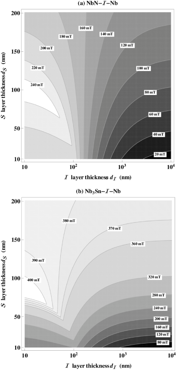
Figure 3: Contour plots of the maximum achievable peak surface-field without vortex dissipations, Bv(ML)superscriptsubscript𝐵𝑣MLB_{v}^{\rm(ML)}. The abscissa represents the {\mathcal{I}} layer thickness dsubscript𝑑d_{\mathcal{I}} and the ordinate represents the 𝒮𝒮{\mathcal{S}} layer thickness d𝒮subscript𝑑𝒮d_{\mathcal{S}}. Values written in the plot area are Bv(ML)superscriptsubscript𝐵𝑣MLB_{v}^{\rm(ML)} in the unit of mT. The top and bottom figures correspond to materials of the 𝒮𝒮{\mathcal{S}} layer. (a) NbNNbN{\rm NbN} (λ1=200nmsubscript𝜆1200nm\lambda_{1}=200\,{\rm nm}, ξ1=5nmsubscript𝜉15nm\xi_{1}=5\,{\rm nm}) and (b) Nb3SnsubscriptNb3Sn{\rm Nb}_{3}{\rm Sn} (λ1=85nmsubscript𝜆185nm\lambda_{1}=85\,{\rm nm}, ξ1=5nmsubscript𝜉15nm\xi_{1}=5\,{\rm nm}), respectively. The bulk superconductor is assumed to be Nb with λ2=40nmsubscript𝜆240nm\lambda_{2}=40\,{\rm nm} and Bvbulk=200mTsuperscriptsubscript𝐵𝑣bulk200mTB_{v}^{\rm bulk}=200\,{\rm mT}.
Refer to caption
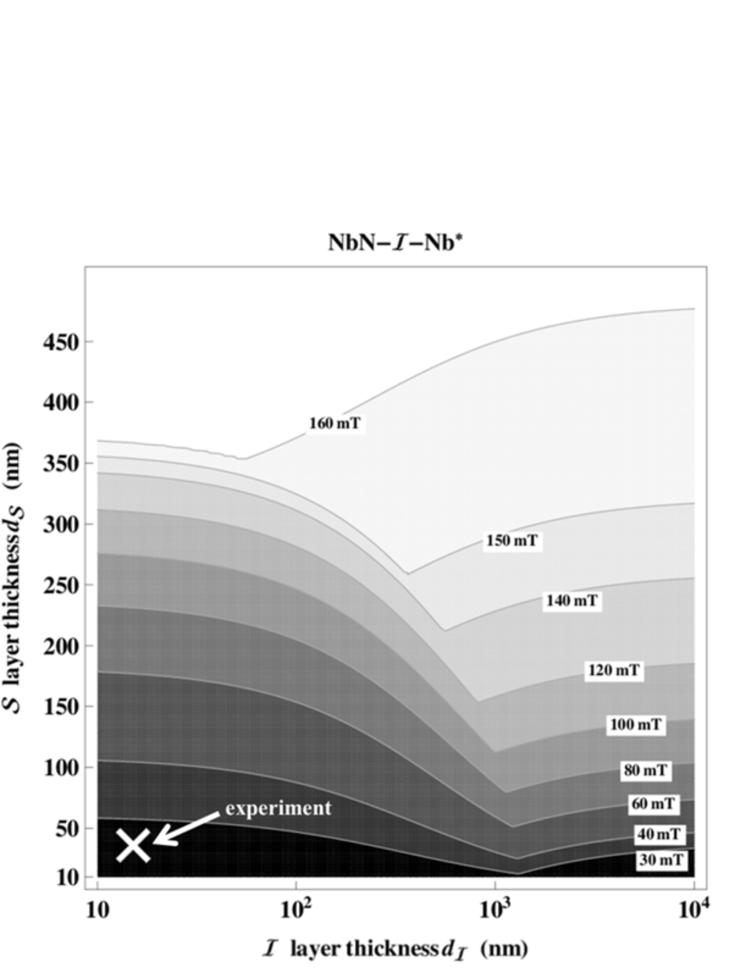
Figure 4: A Contour plot of the maximum achievable peak surface-field without vortex dissipations, Bv(ML)superscriptsubscript𝐵𝑣MLB_{v}^{\rm(ML)}. The abscissa represents the {\mathcal{I}} layer thickness dsubscript𝑑d_{\mathcal{I}} and the ordinate represents the 𝒮𝒮{\mathcal{S}} layer thickness d𝒮subscript𝑑𝒮d_{\mathcal{S}}. Values written in the plot area are Bv(ML)superscriptsubscript𝐵𝑣MLB_{v}^{\rm(ML)} in the unit of mT. Materials of the 𝒮𝒮{\mathcal{S}} layer and the bulk superconductor are assumed to be NbNNbN{\rm NbN} (λ1=200nmsubscript𝜆1200nm\lambda_{1}=200\,{\rm nm}, ξ1=5nmsubscript𝜉15nm\xi_{1}=5\,{\rm nm}) and magnetron sputtered Nb (λ2=300nmsubscript𝜆2300nm\lambda_{2}=300\,{\rm nm} balalykin and Bvbulk=20mTsuperscriptsubscript𝐵𝑣bulk20mTB_{v}^{\rm bulk}=20\,{\rm mT} antoine2 ), respectively. A cross shown at the lower left indicate a parameter set used in an experiment antoine2 .

A thin 𝒮𝒮{\mathcal{S}} layer pushes up Bv(𝒮)superscriptsubscript𝐵𝑣𝒮B_{v}^{(\mathcal{S})}, but it can not protect the bulk superconductor from an applied field if d𝒮λ1much-less-thansubscript𝑑𝒮subscript𝜆1d_{\mathcal{S}}\ll\lambda_{1}. In order to evaluate the achievable peak surface-field without vortex dissipations, not only Bv(𝒮)superscriptsubscript𝐵𝑣𝒮B_{v}^{(\mathcal{S})}, but also the shielded magnetic field on the bulk superconductor must be considered simultaneously. Let us define the magnetic field attenuation ratio α𝛼\alpha by α=BII/B0𝛼subscript𝐵IIsubscript𝐵0\alpha=B_{\rm II}/B_{0}. When the magnetic field attenuation in the 𝒮𝒮{\mathcal{S}} layer is enough for the shielded magnetic field αBv(𝒮)𝛼superscriptsubscript𝐵𝑣𝒮\alpha B_{v}^{(\mathcal{S})} to become smaller than a vortex penetration field of the bulk superconductor, Bv(bulk)superscriptsubscript𝐵𝑣bulkB_{v}^{\rm(bulk)}, the bulk superconductor is safely protected. Then the achievable peak surface-field without vortex dissipations, Bv(ML)superscriptsubscript𝐵𝑣MLB_{v}^{\rm(ML)}, is given by Bv(𝒮)superscriptsubscript𝐵𝑣𝒮B_{v}^{(\mathcal{S})}. On the other hand when the magnetic field attenuation is not enough and αBv(𝒮)𝛼superscriptsubscript𝐵𝑣𝒮\alpha B_{v}^{(\mathcal{S})} is larger than Bv(bulk)superscriptsubscript𝐵𝑣bulkB_{v}^{\rm(bulk)}, Bv(ML)superscriptsubscript𝐵𝑣MLB_{v}^{\rm(ML)} is limited by α1×Bv(bulk)superscript𝛼1superscriptsubscript𝐵𝑣bulk\alpha^{-1}\times B_{v}^{\rm(bulk)}. Thus we find

Bv(ML)={Bv(𝒮)(αBv(𝒮)<Bv(bulk))α1×Bv(bulk)(αBv(𝒮)Bv(bulk)).superscriptsubscript𝐵𝑣MLcasessuperscriptsubscript𝐵𝑣𝒮𝛼superscriptsubscript𝐵𝑣𝒮superscriptsubscript𝐵𝑣bulksuperscript𝛼1superscriptsubscript𝐵𝑣bulk𝛼superscriptsubscript𝐵𝑣𝒮superscriptsubscript𝐵𝑣bulk\displaystyle B_{v}^{\rm(ML)}=\begin{cases}B_{v}^{(\mathcal{S})}&(\alpha B_{v}^{(\mathcal{S})}<B_{v}^{\rm(bulk)})\\ \alpha^{-1}\times B_{v}^{\rm(bulk)}&(\alpha B_{v}^{(\mathcal{S})}\geq B_{v}^{\rm(bulk)}).\end{cases} (5)

Fig. 3 shows Bv(ML)superscriptsubscript𝐵𝑣MLB_{v}^{\rm(ML)} of (a) NbN-{\mathcal{I}}-Nb structure and (b) Nb3SnsubscriptNb3Sn{\rm Nb_{3}Sn}-{\mathcal{I}}-NbNb{\rm Nb} structure. A choice of appropriate parameter regions should improve Bv(ML)superscriptsubscript𝐵𝑣MLB_{v}^{\rm(ML)}: a combination of an NbN layer (Nb3SnsubscriptNb3Sn{\rm Nb_{3}Sn} layer) with d𝒮=100nmsubscript𝑑𝒮100nmd_{\mathcal{S}}=100\,{\rm nm} (90nm90nm90\,{\rm nm}) and an {\mathcal{I}} layer with d=10nmsubscript𝑑10nmd_{\mathcal{I}}=10\,{\rm nm} yields Bv(ML)240mTsimilar-to-or-equalssuperscriptsubscript𝐵𝑣ML240mTB_{v}^{\rm(ML)}\simeq 240\,{\rm mT} (400mT400mT400\,{\rm mT}). Bv(ML)superscriptsubscript𝐵𝑣MLB_{v}^{\rm(ML)} of NbN-{\mathcal{I}}-NbsuperscriptNb{\rm Nb}^{*} structure is shown in Fig. 4, where NbsuperscriptNb{\rm Nb}^{*} represents a magnetron sputtered Nb. A thick 𝒮𝒮{\mathcal{S}} layer (d𝒮λ1much-greater-thansubscript𝑑𝒮subscript𝜆1d_{\mathcal{S}}\gg\lambda_{1}) with arbitrary dsubscript𝑑d_{\mathcal{I}} yields the maximum Bv(ML)=160mT(=Bv(S))superscriptsubscript𝐵𝑣MLannotated160mTabsentsuperscriptsubscript𝐵𝑣subscript𝑆B_{v}^{\rm(ML)}=160\,{\rm mT}\,(=B_{v}^{\mathcal{(}S_{\infty})}). A thin 𝒮𝒮{\mathcal{S}} layer yields a rather small Bv(ML)superscriptsubscript𝐵𝑣MLB_{v}^{\rm(ML)}. In general, a bulk superconductor with λ2>λ1subscript𝜆2subscript𝜆1\lambda_{2}>\lambda_{1}, such as NbsuperscriptNb{\rm Nb}^{*}, suppresses Bv(𝒮)superscriptsubscript𝐵𝑣𝒮B_{v}^{(\mathcal{S})} (see Eq. (4)) and thus Bv(ML)superscriptsubscript𝐵𝑣MLB_{v}^{\rm(ML)}. Table. 2 summarizes optimum parameters and resultant maximum Bv(ML)superscriptsubscript𝐵𝑣MLB_{v}^{\rm(ML)}.

On measurements of Bv(ML)superscriptsubscript𝐵𝑣MLB_{v}^{\rm(ML)}, the magnetic field must be applied on one side of the layers. An experiment antoine2 shows Bv(ML)30mTsimilar-to-or-equalssuperscriptsubscript𝐵𝑣ML30mTB_{v}^{\rm(ML)}\simeq 30\,{\rm mT} for the case of NbN(25nm25nm25\,{\rm nm})-MgO(14nm14nm14\,{\rm nm})-NbsuperscriptNb{\rm Nb}^{*}(250nm250nm250\,{\rm nm}), which agrees well with the above calculation (see Fig. 4). Increasing d𝒮subscript𝑑𝒮d_{\mathcal{S}} or using regular Nb instead of NbsuperscriptNb{\rm Nb}^{*} might drastically improve Bv(ML)superscriptsubscript𝐵𝑣MLB_{v}^{\rm(ML)}.

These calculations are performed on the ideal superconductor and insulator. In real situations, however, the superconductor includes defects and surface roughnesses, and both layers have fluctuations in thickness. Effects of these complicated conditions should be considered in the next step.

As for geometrical conditions, only the electromagnetic field propagates perpendicular to the surface of the layers are considered in this article. When the normal components have non-zero value, additional resonance modes associated with the standing waves confined in the insulator layer would appear. Since the extent of the insulator layer could be as long as the wave length of the operating frequency of the cavity, it is possible that additional resonance modes emerge near the operating frequency. In addition to the above points, variations of geometry and electromagnetic fields in other directions should be considered in accordance with real accelerating cavities. Study on effects from these additional conditions, however, is a future challenge.

References

  • (1) W. Singer, S. Aderhold, A. Ermakov, J. Iversen, D. Kostin, G. Kreps, A. Matheisen, W.-D. Mo¨¨o\ddot{\rm o}ller, D. Reschke, X. Singer et al., Phys. Rev. ST Accel. Beams 16, 012003 (2013).
  • (2) H. Padamsee, J. Knobloch, and T. Hays, RF Superconductivity for Accelerators (John Wiley, New York, 1998)
  • (3) A. Gurevich, Appl. Phys. Lett. 88, 012511 (2006).
  • (4) A. Gurevich, Rev. Accel. Sci. Technol. 5, 119 (2012).
  • (5) C. P. Bean and J. D. Livingston, Phys. Rev. Lett. 12, 14 (1964).
  • (6) T. Tajima, in Proceedings of 2011 Particle Accelerator Conference, New York, NY, USA, p. 2119; T. Tajima, H. Inoue, N. F. Haberkorn, L. Civale, R. K. Schulze, J. Guo, V. A. Dolgashev, D. W. Martin, S. G. Tantawi, C. G. Yoneda et al., in Proceedings of SRF2011, Chicago, IL USA, p. 287; T. Tajima, N. Haberkorn, L. Civale, G. Eremeev, M. Hawley, R. Schulze, A. Zocco, J. Guo, V. Dolgashev, D. Martin et al., in Proceedings of Linear Accelerator Conference LINAC2010, Tsukuba, Japan, p. 854; T. Tajima, G. Eremeev, G. Zou, V. Dolgashev, D. Martin, C. Nantista, S. Tantawi, C. Yoneda, B. H. Moeckly, and I. Campisi, J. Phys. Conf. Ser. 234, 012043 (2010); T. Tajima, G. V. Eremeev, F. L. Krawczyk, in Proceedings of SRF2009, Berlin, Germany, p. 198.
  • (7) C. Z. Antoine, S. Berry, S. Bouat, J-F. Jacquot, J-C. Villegier, G. Lamura, and A Gurevich, Phys. Rev. ST Accel. Beams 13, 121001 (2010); C. Z. Antoine, S. Berry, Q. Famery, J. Leclerc, J-C. Villegier, G. Lamura, and A. Andreone, in Proceedings of SRF2011, Chicago, IL USA, p. 281; C. Z. Antoine, A. Aguilal, S. Berry, S. Bouat, J-F. Jacquot, J-C. Villegier, G. Lamura, and A Gurevich, in Proceedings of SRF2009, Berlin, Germany, p. 401.
  • (8) M. Tinkham, Introduction to Superconductivity (McGraw-Hill, Inc., New York, 1975).
  • (9) T. Kubo, Y. Iwashita, and T. Saeki, in Proceedings of IPAC13, Shanghai, China, p. 2343, http://accelconf.web.cern.ch/AccelConf/IPAC2013/papers/wepwo014.pdf.
  • (10) T. Behnke, J. E. Brau, B. Foster, J. Fuster, M. Harrison, J. M. Paterson, M. Peskin, M. Stanitzki, N. Walker, and H. Yamamoto, ILC Technical Design Report, Vol. 1.
  • (11) T. Kubo, Y. Iwashita, and T. Saeki, arXiv:1307.0583 [physics.acc-ph].
  • (12) N. I. Balalykin and A. B. Kuznetsov, in Proceedings of SRF1997, Abano Terme (Padova), Italy, p. 366.
  • (13) C. Z. Antoine, J.-C. Villegier, and G. Martinet, Appl. Phys. Lett. 102, 102603 (2013).