Ferroelectric nanodomains in epitaxial PbTiO3 films grown on SmScO3 and TbScO3 substrates
Abstract
Domain structures of 320 nm thin epitaxial films of ferroelectric PbTiO3 grown by MOCVD technique in identical conditions on SmScO3 and TbScO3 perovskite substrates have been investigated by Raman spectroscopy and piezoresponse force microscopy techniques. Phonon frequency shifts and typical domain structure motifs are discussed. The results reveal strikingly different domain structure architecture: domain structures of the PbTiO3 film grown on SmScO3 have dominantly -domain orientation while strongly preferential -domain orientation was found in the PbTiO3 film grown on the TbScO3 substrate. Differences between the two cases are traced back to the film-substrate lattice mismatch at the deposition temperature.
pacs:
77.80.-e,77.80.Dj,68.55.-a,68.37.PsI Introduction
Morphology of domain structure in thin films of tetragonal ferroelectric perovskite oxides has recently attracted a considerable amount of interest.Book2 ; Ganpule02 ; Roytburd01 ; Alpay98III ; Koukhar01 ; Pertsev98 ; streiff02 ; Schilling06 Various special patterns were seen, such as ferroelectric flux closure and quadrupolar vortex arrangements.Fu03 ; Scott05 ; Prosandeev06 ; Gruverman08 ; Rodriguez09 ; McGillyNano10 ; Ivry10 ; McGillyJMS09 ; SchillingPRB11 ; SchillingNano09 ; McQuaid11 Most peculiar domain arrangements were found in theoretical model simulations conducted for rather extreme geometries of dimensions comparable with domain wall thickness, such as ultrathin films, short-period superlattices and ferroelectric nanodots.Fu03 ; Scott05 ; Prosandeev06 ; Rodriguez09 Domain walls in ferroelectric films with an order of magnitude larger thickness (of the order of 100 nm) are expected to bear mostly bulk material properties. Nevertheless, the necessity of stress and depolarization charge compensation at 100 nm scales implies presence of a much higher density of domain walls and this can also make conditions for certain nanoscale-specific domain arrangements, different from typical bulk domain structures.
The key factor dictating the domain structure type in epitaxial ferroelectric films is the lattice misfit strain. In general, compressive stress favors so-called c-domain states with out-of-plane polarization orientation, while tensile stress favors a-domain states with in-plane polarization orientation. However, the relative weights of ferroelastic domain variants in the domain structure is not the only mechanism for relieving the misfit stresses. Typically, in case of epitaxial ferroelectric films with thicknesses of 50-500 nm, a considerable amount of epitaxial stress is relaxed by formation of dislocations. Therefore, the final domain structure may depend on a number of other factors, such as growth temperature and annealing history.Book2 ; Speck94I ; Speck94II ; Alpay98III Perspective of practical applications of such thin ferroelectric films, for example in so-called MEMS devices, obviously calls for a better insight in the processes governing the formation of their domain texture. As a contribution to this problem, we present here investigations of PbTiO3 (PTO) epitaxial thin films grown on two different high quality rare earth scandate crystal substrates. Interestingly, although these films were prepared simultaneously in the same MOCVD deposition process, the resulting nanodomain architecture of these thin films is drastically different.
II Experimental
The PTO thin film samples for this investigation were grown by pulsed injection metal-organic chemical vapor deposition (MOCVD) technique on commercial high-quality (110)-oriented TbScO3 (TSO) and SmScO3 (SSO) single crystal substrates developed for epitaxial deposition of perovskite materials.SchlomAnnu07 Deposition took place at about 650 ∘C (for other details, see e.g. Refs. barta1, ; barta2, ). Films were deposited on both substrates simultaneously to avoid possible differences in the deposition history. Preliminary room-temperature X-ray diffraction taken just after the growth clearly indicated single-crystalline epitaxy with preferential -domain orientation in the film grown on TSO (less than 10 volume percent of residual -domains) and preferential -domain orientation in the film grown on SSO (with about 6 volume percent of residual -domains). Thickness of the resulting PTO films (about 320 nm) was determined on another film (grown on Si substrate during the same deposition), which was etched with concentrated HF to form a step for thickness measurement by profilometry. All present measurements were done at ambient conditions on as-grown films, no thermal cycles were done after.
The piezoresponse force microscopy (PFM) measurements were conducted using the atomic force microscope (AFM) of the Ntegra spectra apparatus operated with a conductive tip (TiN-coated n-doped silicon cantilever) in a contact mode. Using silver paste, the samples were carefully glued to a special plate provided with a spring contact. The frequency of the alternating voltage was set to a value of 15 kHz and the amplitude to 5 V. The mechanical response of the cantilever-tip-surface system detected in a standard way was amplified and analyzed with an external SR830 DSP Lock-In Amplifier.
Polarized Raman spectra were measured using Renishaw Raman RM-1000 Micro-Raman spectrometer with a CCD detection. The experiments were performed in backscattering geometry in the 20-900 cm-1 range. The 514.5 nm line of an Ar+ ion laser was focused to a spot size of about 2 m. The VV and HV polarization configurations correspond to situations where the input and output light polarizations are parallel and crossed, respectively. TbScO3 and SmScO3 substrates have several Raman modes within the region of interest. Consequently, the spectra contained modes of the substrate as well as of the material and were difficult to analyze. To obtain pure film spectra, substrate spectra were measured separately and the substrate contribution was subtracted from film+substrate spectra.
III Results
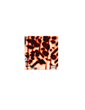
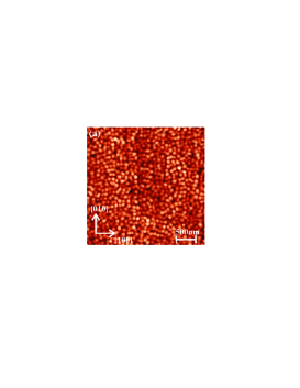
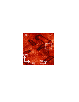
Typical AFM images of the investigated PTO films are shown in Fig. 1 and Fig. 2. The topographic imaging mode has shown a gentle surface corrugation. The morphology of this roughness can be described as a dense disordered pattern of few nm high circular protuberances, indicating an island growth mechanism, frequently encountered in MOCVD deposition.barta4 The surface topography of the film grown on TSO substrate is very similar to the film grown on SSO substrate. However, the PFM images are quite different. The PFM images of PTO/TSO film reveal dominantly -domain signal with narrow minor -type domains in a arrangements, while the film grown on SSO substrate is mostly showing only -domains arranged in stripes revealing fine structure of (110) and (1) oriented 90-degree walls.
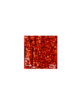
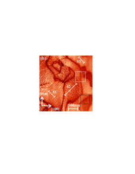
For example, the basic motif of the vertical-signal PFM image of PTO film on TSO shown in Fig. 1 appear to be the ”Swedish ladder” pattern formed by quasi-regular alternations of about 100 nm wide -c-domain stripes with an order of magnitude narrower -domain stripes (faint-contrast ”bars” of the Swedish ladder). This pattern is very similar to the domain arrangements reported for PTO films grown on Nd-doped SrTiO3 (STO) substrates.LeeChoiLeeBaik01 Another, less dense set of about 150 nm thick stripes (vertical on Fig. 1, intermediate darkness) has been also observed in PTO films grown on STO substratesLeeChoiLeeBaik01 and it can be assigned to a minor fraction of lamellae.Nakaki08 ; Nakaki09 ; Utsugi09 Finally, the kidney-shaped (dark) islands with about 100 nm diameter correspond to the inverted structure with opposite overall spontaneous polarization. Consequently, the borders of these islands are mostly formed by 180-degree domain walls. These 180-degree domain interfaces help to minimize the depolarization fields normal to the film. This is likely the reason why they do not form spontaneously on conductive substrates like Nd-doped STO. However, similar density and pattern of 180-degree walls was observed in PTO films grown on LaAlO3 (LAO) substrates.Simon11
The orientation of polarization in PTO films grown on SSO can be identified by the analysis of the PFM signal in the vertical and the lateral mode. The long axis of the AFM cantilever was parallel to the [010] direction indicated in Fig. 2, so that the contrast of the lateral PFM images is mostly given by the [100] polarization component. Since the polarization is almost exclusively in-plane oriented in most of the images, the vertical PFM images give mainly contrast along the [010] axis (due to the cantilever buckling effect).Buckling1 ; Buckling2 ; Buckling3 Comparison of lateral and vertical mode images taken in the same area clearly confirms presence of about 0.5-1 micron size ”coarse domains” formed by regular nanodomain twinned areas with about 20 nm wide -domain stripes with polarization oriented alternatively along [100] and [010] axes. These patterns are very similar to the domain structure seen on PTO films grown on KTaO3 (KTO) crystal substrates.LeeChoiLeeBaik01 It is natural to expect that these stripes are separated by mechanically and electrically compatible head-to-tail 90-degree domain walls normal to either [110] or [1].
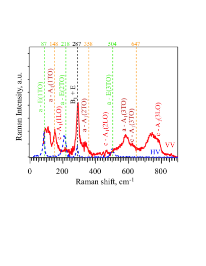
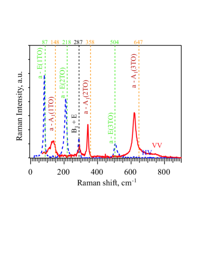
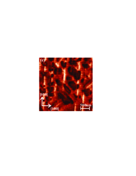
The preferential -domain and -domain occurrence in PTO films grown on TSO and SSO films, respectively, can be also documented by polarized Raman spectroscopy. Typical backscattering Raman spectra taken from the PTO/TSO sample surface in and geometry (after subtraction of the substrate signal) are shown in Fig. 3. Similar spectra for PTO/SSO sample are shown in Fig. 4. Modes can be assigned by comparison with previous measurements on PbTiO3 films.barta3 The basic rule here is that according to the standard selection rules for symmetric Raman tensors, the pure phonon modes (with dynamical charge fluctuating along the tetragonal axis) should be active in the spectra but not in the spectra, while the pure modes (with dynamical charge fluctuating perpendicular to the tetragonal axis) should be active only in the spectra. The presence of strong Raman bands close to frequencies of bulk PbTiO3 (for example, the band near 770 cm-1) thus suggests a large volume of areas with tetragonal axis normal to the film (-domains). In contrast, the band is barely seen in the similar spectrum taken from the PTO film grown on SSO substrate, confirming in this way a negligible volume of the -domain in such sample. Moreover, modes from -domains should not be active either in the or in the spectrum. Therefore, only the modes from -domains are observed in the adopted backscattering geometry. Since there is only a minute fraction of -domains in TSO-grown film, the spectrum of the TSO-grown sample is indeed quite weak.
IV Discussion
Using three different techniques (X-ray diffraction, PFM imaging and Raman spectroscopy) we have seen that the tetragonal axis of the PTO has a dominant in-plane orientation in case of films grown on SSO substrate, while, on the other hand, it is clearly preferentially perpendicular to the film in case of the TSO substrates. The room-temperature pseudo-cubic lattice parameters of both substrates (about 3.960 and 3.985 Å for TSO and SSO, resp.)Uecker08 are both between the and room-temperature lattice parameters of bulk tetragonal PTO (about 3.90 and 4.155 Å).Mabud79 Therefore, a perfect atomic epitaxy should lead to a tensile epitaxial stress in -domains and biaxial in-plane strain in -domains (compressive local stress in PTO lattice along its in-plane-oriented tetragonal axis, tensile stress in the other direction in the plane of the film).
However, these naive considerations neglect the effect of other factors like thermal expansion and formation of dislocations during the deposition. Therefore, it is instructive to examine possible stress-induced phonon frequency shifts in the recorded Raman spectra. For this purpose, we have marked the positions of the known stress-free bulk phonon frequencies directly in our Raman spectra. Phonon frequency shifts are particularly clear in the case of the film grown on SSO: all (TO) modes in the dominant -domain configuration show a considerable frequency downshift with respect to the bulk mode frequencies (about 30 cm-1). Such shifts are quite unusual for a 320 nm thick film; in fact, comparable frequency shifts were reported in the case of -domains in PTO films grown on LaAlO3, but only when the films were about one order of magnitude thinner.barta4 As it is known that uniaxial compression of PTO along the tetragonal axis decreases all (TO) modes (see, for example Ref. Marton13, ), the observed Raman shifts suggest that -domains are really under compression along the local tetragonal axis there. On the contrary, (TO) modes in the dominant -domain configuration show much smaller shifts, what could be an indication of the expected local biaxial in-plane epitaxial strain.
Although we do not fully understand the decisive criteria for the formation of such a nicely strained PTO film with structure, we believe that the essential difference between the TSO and SSO substrate in this respect is that the high-temperature PTO film growth on SSO substrate occurs in conditions of a slight tensile straining. In fact, the only other case of PTO epitaxial film with a very similar domain structure known to us is that of PTO film grown on KTO substrate,LeeChoiLeeBaik01 which happens to have a lattice constant very similar to SSO (room-temperature lattice parameter of KTO is about 3.99 Å).SchlomAnnu07 On the contrary, the TSO substrate and most of the other popular substrates (STO, LAO, (LaxSr1-x)(AlyTa1-y)O3) have a smaller lattice constant than the cubic PTO at 650 ∘C.
Indeed, pseudocubic lattice parameter of bulk SSO at 650 ∘C = 4.01 Å (evaluated using linear thermal expansion coefficient and room temperature lattice constant from Ref. Uecker08, ), while that of bulk TSO at 650 ∘C is only = 3.96 Å (also evaluated using linear thermal expansion coefficient and room temperature lattice constant from Ref. Uecker08, ). Therefore, the lattice parameter of bulk cubic PTO at 650 ∘C = 3.99 Å (extrapolated from data of Ref. Mabud79, ) falls in between that of TSO and SSO () and perfect epitaxial matching would imply that thin PTO films grown on TSO and SSO exhibit at growing conditions compressive and tensile biaxial in-plane strain respectively. Such strain is rather large in case of the 300 nm thick film, and, most likely, it is partly reduced by formation of dislocations.
At and below the ferroelectric phase transition (near 500 ∘C), the ”natural” lattice parameters of bulk PTO are modified by spontaneous strain, and this has most significant impact on the local lattice mismatch variation on cooling. Since the spontaneous lattice strain is considerable in bulk PTO ( parameter is by 6 percent larger than the parameter at room temperature), the average in-plane lattice parameter of PTO film obviously strongly depends on the volume ratio of domains with different -axis orientation. At a first approximation, the twinned area would have average in-plane lattice parameter , i.e. about 4.03 Å at room temperature, which is by 3 percent more than the natural in-plane lattice constant of a single domain PTO film with -axis vertical (=3.90 Å at room temperature). The actual domain formation process probably involves nucleation and motion of ferroelectric domain walls as well as lattice dislocations, but its details are not obvious to us.
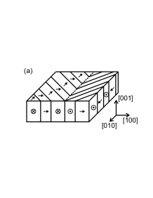
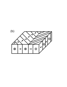
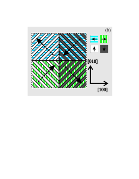
It is also interesting to note that the domain structure observed in the PTO films grown on SSO happens to be similar to the domain structures observed in the focused-ion-beam-cut free-standing lamellae of BaTiO3 single crystals.Schilling06 In both cases, the present PTO film and BTO lamellae, the areas of quasi-regular pattern motifs are forming larger-scale ”mesoscopic” domains, separated by narrow interfaces, which can be considered as ”mesoscopic domain walls”. Like the true ferroelectric boundaries, these mesoscopic domain walls shows a clear directional preferences - they tend to be parallel to the [100] and [010] directions or close to [110] and [10] directions. Idealized microstructure of such [010] mesoscopic boundary between two domains is sketched in Fig. 5. The mesoscopic boundary in Fig. 5(a) in fact corresponds to a sequence of (charge and mechanically compatible) 180-degree ferroelectric domain walls with [010] orientation and ”no-wall” regions, where local domain state is not changed at all. On the other hand, the mesoscopic boundary in Fig. 5(b) is formed by a sequence of 90-degree walls, which are locally in a electrically and mechanically incompatible arrangement,Janovec69 ; Marton10 even though the overall mesoscopic boundary can be in both cases considered as a charge-neutral head-to-tail boundary. We have not seen any clear preference for the structure of Fig. 5(a) in our images, probably also because it requires identical twinning period in the adjacent mesoscopic domains. Nevertheless, the TEM image of the corresponding mesoscopic boundary in PTO film grown on KTO seems to support preference for the structure of Fig. 5(b) (see Fig. 10 of Ref. LeeChoiLeeBaik01, ).
The structure of mesoscopic boundaries oriented along [110] direction is shown in Fig. 6, obtained by zooming from Fig. 2. Here the boundary is clearly formed by an array of wedge-type nanodomain terminations, rather than by any type of known flat compatible domain walls. This observation strongly reminds the ”bundle boundary” observed in BaTiO3 lamellae.McGillyNano10 In principle, however, the mesoscopic domain boundary could be formed by mechanically compatible uncharged 180-degree domain walls, as proposed in Fig. 6(b).

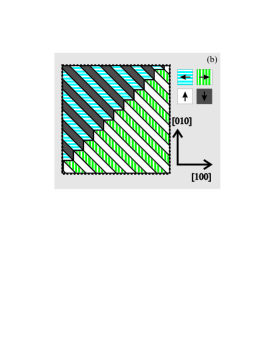
In the present experiment we also observed several mesosocopic domain intersections. The intersection of two mesoscopic domain walls oriented along [100] and [010] direction forms an interesting object which is probably quite analogous to the ”quadrant-quadrupole” mesosocopic domain structures known from BaTiO3 lamellae.SchillingPRB11 Example of such quadrant-quadruple mesoscopic domain structure, obtained by zooming from Fig. 2(b), is shown in Fig. 7.
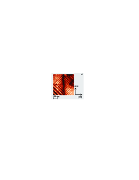
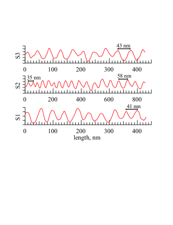
Finally, Fig. 8 shows several representative scans through PFM data, allowing to extract quantitative information about nanodomain periods. The period fluctuates between mesoscopic domains as well as within single domains; but the average nanodomain size of 20-30 nm roughly agrees with the values expected from Kittel’s law for a 320 nm thick plate.Catalan07 ; streiff02
V Conclusion
Epitaxial films of ferroelectric PbTiO3, about 320 nm thick, have been simultaneously deposited by MOCVD technique on two different scandate single crystal substrates. Subsequent X-ray, PFM and Raman confirmed that PTO films grown on TSO have preferentially -domain orientation, while films grown on SSO have dominantly -domain orientation (in-plane orientation of spontaneous polarization). The striking difference between the two domain structures is assigned to the opposite sign of the epitaxial misfit strain at the deposition temperature. The strained PTO films grown on SSO substrate shows interesting domain arrangements analogous to the structures reported in free-standing BaTiO3 single crystal lamellae. We believe that these results will be useful for understanding and design of epitaxial ferroelectric films with thickness of about 300 nm.
Acknowledgements.
This work was supported by the Czech Science Foundation (Projects Project GACR P204/10/0616 and 202/09/H0041) and EGIDE (Grant No. GILIBERT 25536 WF). In addition, the contribution of Ph.D. student F. Borodavka has been supported by Czech Ministry of Education (project SVV-2012-265303).References
- (1) A. K. Tagantsev, L. E. Cross, and J. Fousek, Domains in Ferroic Crystals and Thin Films (Springer, New York, 2010).
- (2) C. S. Ganpule, V. Nagarajan, B. K. Hill, A. L. Roytburd, E. D. Williams, R. Ramesh, S. P. Alpay, A. Roelofs, R. Waser, and L. M. Eng, J. Appl. Phys. 91, 1477 (2002).
- (3) A. L. Roytburd, S. P. Alpay, L. A. Bendersky, V. Nagarajan, and R. Ramesh, J. Appl. Phys. 89, 553 (2001).
- (4) S. P. Alpay and A. L. Roytburd, J. Appl. Phys. 83, 4714 (1998).
- (5) V. G. Koukhar, N. A. Pertsev, and R. Waser, Phys. Rev. B 64, 214103 (2001).
- (6) N. A. Pertsev, A. G. Zembilgotov, and A. K. Tagantsev, Phys. Rev. Lett. 80, 1988 (1998).
- (7) S. K. Streiffer, J. A. Eastman, D. D. Fong, C. Thompson, A. Munkholm, M. V. Ramana Murty, O. Auciello, G. R. Bai, and G. B. Stephenson, Phys. Rev. Lett. 89, 067601 (2002).
- (8) A. Schilling, T. B. Adams, R. M. Bowman, J. M. Gregg, G. Catalan, and J. F. Scott, Phys. Rev. B 74, 024115 (2006).
- (9) H. Fu and L. Bellaiche, Phys. Rev. Lett. 91, 257601 (2003).
- (10) J. F. Scott, Nature Materials 4, 13 (2005).
- (11) S. Prosandeev, I. Ponomareva, I. Kornev, I. Naumov, and L. Bellaiche, Phys. Rev. Lett. 96, 237601 (2006).
- (12) A. Gruverman, D. Wu, H.-J. Fan, I. Vrejoiu, M. Alexe, R. J. Harisson, and J. F. Scott, J. Phys.: Condens. Matter 20, 342201 (2008).
- (13) B. J. Rodriguez, X. S. Gao, L. F. Liu, W. Lee, I. I. Naumov, A. M. Bratkovsky, D. Hesse, and M. Alexe, Nano Lett. 9, 1127 (2009).
- (14) L. J. McGilly, A. Schilling, and J. M. Gregg, Nano Lett. 10, 4200 (2010).
- (15) Y. Ivry, D. P. Chu, J. F. Scott, and C. Durkan, Phys. Rev. Lett. 104, 207602 (2010).
- (16) L. McGilly, D. Byrne, C. Harnagea, A. Schilling, and J. M. Gregg, J. Mat. Sci 44, 5197 (2009).
- (17) A. Schilling, S. Prosandeev, R. G. P. McQuaid, L. Bellaiche, J. F. Scott, and J. M. Gregg, Phys. Rev. B 84, 064110 (2011).
- (18) A. Schilling, D. Byrne, G. Catalan, K. G. Webber, Y. A. Genenko, G. S. Wu, J. F. Scott, and J. M. Gregg, Nano Lett. 9, 3359 (2009).
- (19) R. G. P. McQuaid, L. J. McGilly, P. Sharma, A. Gruverman, and J. M. Gregg, Nature Communications 2, 404 (2011).
- (20) J. S. Speck and W. Pompe, J. Appl. Phys. 76, 466 (1994).
- (21) J. S. Speck, A. Seifert, W. Pompe, and R. Ramesh, J. Appl. Phys. 76, 477 (1994).
- (22) D. G. Schlom, L.-Q. Chen, C.-B. Eom, K. M. Rabe, S. K. Streiffer, and J.-M. Triscone, Annu. Rev. Mater. Res. 37, 589 (2007).
- (23) A. Bartasyte, A. Abrutis, C. Jimenez, F. Weiss, O. Chaix-Pluchery, and Z. Saltyte, Ferroelectrics 353, 104 (2007).
- (24) A. Bartasyte, R. Bouregba, E. Dogheche, M. Boudard, G. Poullain, O. Chaix-Pluchery, C. Jimenez, V. Plausinaitiene, D. Remiens, A. Abrutis, Z. Saltyte, and F. Weiss, J. Surf. Coat. Technol. 201, 9340 (2007).
- (25) A. Bartasyte, O. Chaix-Pluchery, J. Kreisel, C. Jimenez, F. Weiss, A. Abrutis, Z. Saltyte, and M. Boudard, J. Appl. Phys. 103, 014103 (2008).
- (26) K. S. Lee, J. H. Choi, J. Y. Lee, and S. Baik, J. Appl. Phys. 90, 4095 (2001).
- (27) H. Nakaki, Y. K. Kim, S. Yokoyama, R. Ikariyama, H. Funakuba, S. K. Streiffer, K. Nishida, K. Saito, and A. Gruverman, J. Appl. Phys. 104, 064121 (2008).
- (28) H. Nakaki, Y. K. Kim, S. Yokoyama, R. Ikariyama, H. Funakubo, K. Nishida, K. Saito, H. Morioka, O. Sakata, H. Han, and S. Baik, J. Appl. Phys. 105, 014107 (2009).
- (29) S. Utsugi, T. Fujisawa, R. Ikariyama, S. Yasui, H. Nakaki, T. Yamada, M. Ishikawa, M. Matsushima, H. Morioka, and H. Funakubo, Appl. Phys. Lett. 94, 052906 (2009).
- (30) E. Simon, F. Borodavka, I. Gregora, D. Nuzhnyy, S. Kamba, J. Hlinka, A. Bartasyte, and S. Margueron, J. Appl. Phys. 110, 084115 (2011).
- (31) E. Soergel, J. Phys. D: Appl. Phys. 44, 464003(2011).
- (32) T. Jungk, A. Hoffmann, and E. Soergel, New Journal of Physics 11, 033029 (2009).
- (33) R. Nath, S. Hong, J. A. Klug, A. Imre, M. J. Bedzyk, R. S. Katiyar, and O. Auciello, Appl. Phys. Lett. 96, 163101 (2010).
- (34) A. Bartasyte, S. Margueron, J. Santiso, J. Hlinka, E. Simon, I. Gregora, O. Chaix-Pluchery, J. Kreisel, C. Jimenez, F. Weiss, V. Kubilius, and A. Abrutis, Phase Transitions 84, 509 (2011).
- (35) R. Uecker, B. Velickov, D. Klimm, R. Bertram, M. Bernhagen, M. Rabe, M. Albrecht, R. Fornari, and D. G. Schlom, Journal of Crystal Growth 310, 2649 (2008).
- (36) S. A. Mabud and A. M. Glazer, J. Appl. Crystallogr. 12, 49 (1979).
- (37) P. Marton and J. Hlinka, Phase Transitions 86, 200 (2013).
- (38) J. Fousek and V. Janovec, J. Appl. Phys. 40, 135 (1969).
- (39) P. Marton, I. Rychetsky, and J. Hlinka, Phys. Rev. B 81, 144125 (2010).
- (40) G. Catalan, J. F. Scott, A. Schilling, and J. M. Gregg, J. Phys.: Condens. Matter 19, 022201 (2007).