Engineering Nanowire n-MOSFETs at 8 nm
Abstract
As metal-oxide-semiconductor field-effect transistors (MOSFET) channel lengths () are scaled to lengths shorter than 8 nm source-drain tunneling starts to become a major performance limiting factor. In this scenario a heavier transport mass can be used to limit source-drain (S-D) tunneling. Taking InAs and Si as examples, it is shown that different heavier transport masses can be engineered using strain and crystal orientation engineering. Full-band extended device atomistic quantum transport simulations are performed for nanowire MOSFETs at 8 nm in both ballistic and incoherent scattering regimes. In conclusion, a heavier transport mass can indeed be advantageous in improving ON state currents in ultra scaled nanowire MOSFETs.
Index Terms:
Source-Drain tunneling, nanowire, Si, InAs, strain, quantum transport, tight-binding (TB) approach.I Introduction
Scaling of complementary metal-oxide-semiconductor (CMOS) technology for the past fourty years has led to current device technology with channel lengths well below 30 nm [1]. The International Technology Roadmap for Semiconductors (ITRS) predicts MOSFET channel lengths to be less than 8 nm in ten years [2]. In this extremely scaled regime, MOSFETs will suffer from excessive source - drain (S-D) tunneling, making it hard to turn off the device [3, 4]. Nanowire based MOSFETs have emerged as promising candidates for future scaling as they offer the best electrostatic gate control over the channel [5]. Nanowire MOSFETs made from high mobility III-V materials are being projected as the future of microelectronics [6]. However, it remains an open question how practical it would be to scale MOSFETs to channel lengths below 8 nm. In such extremely scaled regime of operation, it becomes clear that the most critical aspect is to maintain good sub-threshold characteristics.
The typical transistor approach prefers a light transport mass corresponding to high carrier velocities and a heavy confinement mass for higher quantum capacitance () [7]. A light transport mass, however, leads to an increased source drain tunneling and can lead to degraded OFF state characteristics [8]. A heavy transport mass can limit S-D tunneling but it also means lower channel mobility or degraded ON state characteristics. This situation naturally leads to a trade-off and begs the question - what transport mass will work the best for ultra scaled channel MOSFETs and can it be engineered?
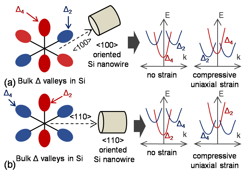
This work shows that different conduction band (CB) minima masses can be obtained in nanowire channels using strain and orientation engineering and how these changes will affect the transistor performance. In a Si nanowire, due to quantum confinement, the six bulk valleys rearrange themselves in energy, with each equivalent set of valleys forming its own separate ”energy ladder” . Furthermore, the different sets of ”energy ladders” can be ”rearranged’ in energy space using uniaxial strain leading to different band edge transport masses (Fig. 1). InAs as a channel material is also considered in this study as a candidate for ”high-mobility material”. Full band quantum transport calculations are used to assess the ON state ballistic and electron-phonon scattering limited device performance for the different CB minima mass nanowire devices. The simulation results suggest that for scaling of the channel lengths below 8 nm, increasing the transport mass leads to better device performance.
II Simulation Approach
II-A Nanowire cases considered in this study
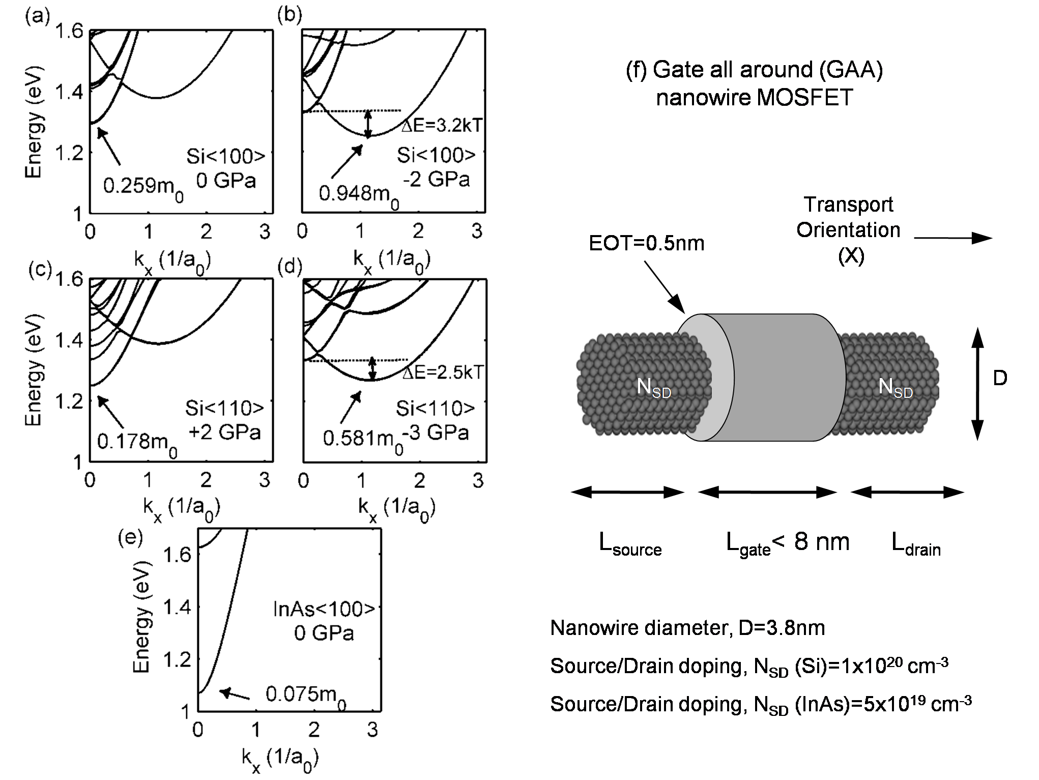
Five different nanowire MOSFET cases are studied in this paper. At sub-8 nm channel lengths, a smaller diameter is critical for an increased gate control. At the same time, however, a smaller diameter leads to increased threshold voltage fluctuation due to process variations. Considering these issues, an optimal diameter, D=3.8 nm, is used for all the simulations [9]. As a first step the different CB minina mass conditions that can be achieved in Si and InAs nanowires are discussed.The applied stress values were chosen to be high enough such that the bottom-most band is energetically at least 2kT lower than the next higher sub-band, while at the same time ensuring the stress values are experimentally achievable [10].
II-A1 Unstrained Si 100
Fig. 2(a) shows the case for an unstrained <100>oriented Si nanowire where the set of valleys form the CB minima . The CB minima effective mass is calculated to be 0.259.
II-A2 Compressive stressed Si 100
Unstrained Si 100 nanowire exhibits valleys that have a heavy transport mass but lie higher in energy due to its lighter confinement mass. On application of compressive stress the heavy valleys are pulled down in energy leading to CB minima mass of 0.948 as shown in Fig. 2(b).
II-A3 Tensile stressed Si 110
Fig. 2(c) shows the E-k relation for a tensile stressed 110 oriented Si nanowire. This case is close to current n-MOS technology where tensile stress is used to reduce CB minima mass and increase the energy difference between the lighter and heavier valleys [10, 1]. The CB minima mass for a 110 oriented nanowire with an applied tensile stress of 2 GPa is calculated to be 0.178.
II-A4 Compressive stressed Si 110
On applying a compressive stress along Si 110 transport direction, heavier valleys are pulled down increasing the CB minima mass. As the stress type is reveresed to compressive 3 GPa, the CB minima mass increases to 0.581 from 0.178 as shown in Fig. 2(d).
II-A5 Unstrained InAs 100
High mobility materials with high In% are being actively researched as a post-Si channel material [6]. In light of this fact a 100 oriented InAs channel is also considered in this study. Fig. 2(e) shows the E-k, with a calculated band edge mass of 0.075.
II-B Transport Simulation
Transport simulations are performed using a full-band quantum transport simulator based on the tight-binding model in the nearest neighbour approximation (without spin-orbit coupling). The atomistic Schrodinger-Poisson equations are solved self-consistently in the nonequilibrium Green function formalism at room temperature [11, 12, 13, 14]. The electron-phonon scattering is computed in the self-consistent Born approximation that couples the full electron and confined phonon spectra [15]. An effective oxide thickness (EOT) equal to 0.5 nm is used for all the simulations [2]. The oxide layers are treated as perfect insulator and hard wall boundary conditions are applied to the surface Si atoms. A source/drain doping level of 1 is assumed for Si nanowires while 5 is the doping level for the InAs nanowire.
Nanowire gate all around (GAA) n-MOSFETs are simulated for the five different CB minima mass cases (Figs. 2(a)-(e)) at channel lengths of 3, 5 and 7 nm as shown in Fig. 2(f). The OFF state current () is set to (= at and ), where the current has been normalized by the diameter [2]. Transfer characteristics of the different nanowire MOSFETs are compared at a supply voltage =0.5V.
III S-D tunneling and subthreshold characteristics
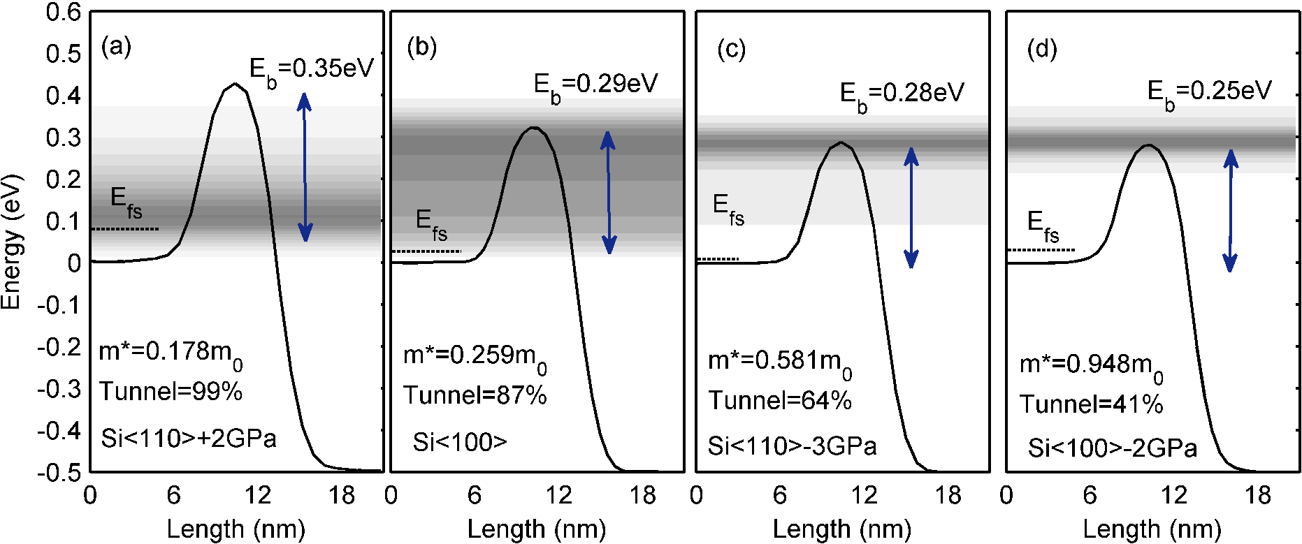
The S-D tunneling is a quantum mechanical phenomenon that is fundamental and cannot be avoided. Fig. 3 illustrates the OFF state current profile for the different CB minima cases at =5 nm simulated in the ballistic regime. For the heaviest mass case it can be seen that most of the current flows over the barrier as opposed to the lightest mass case where most of the current quantum-mechanically tunnels through the barrier. The amount of current flowing below the potential barrier height () is the tunneling current (). The ratio of to the total current or the , increases as the CB minima mass becomes lighter. As a consequence of increased S-D tunneling, to achieve the desired OFF state current the barrier height needs to be raised much more for a light transport mass as compared to a heavy transport mass case. This leads to an increased SS in presence of S-D tunneling.
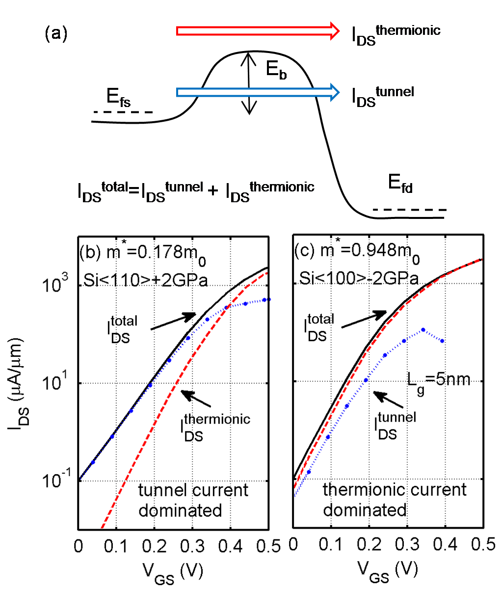
Fig. 4(a) shows the tunnel component () along with the current flowing over the barrier or the thermionic component () during a MOSFET operation. Bias dependent current components for a light transport mass case (equivalent to Fig. 2(c)) is shown in Fig. 4(b) and a for heavy transport mass case (equivalent to Fig. 2(b)) is shown in Fig. 4(c), both at nm. The adverse effect of S-D tunneling in the presence of a light CB minima mass becomes clear as the subthreshold current is totally dominated by . On the other hand, subthreshold slope is controlled by current for the heavy CB minima mass case, bringing it closer to the classical MOSFET operation where the electrostic gate control determines the subthreshold characteristics.
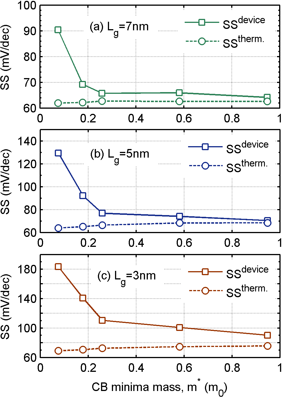
The calculated subthreshold characteristics for the different CB minima cases at different channel lengths are shown in Fig. 5. The subthreshold slope calculated from is labelled as while is the actual subthreshold slope of the nanowire MOSFET calculated in presence of S-D tunneling. It can be readily observed that for light CB minima mass cases the and show a huge difference. As the CB minima mass increases, the and values begin to merge. This can be understood from the fact that with a heavy CB minima mass the electrostatic gate control determines the subthreshold slope. As the CB minima mass becomes lighter the S-D tunneling component begins to dominate. This fact also underlines another important understanding that the lower limit of SS=60 mV/dec at room temperature does not hold anymore in presence of S-D tunneling. With the best of gate control, the amount of S-D tunneling will set the lower limit on the achievable SS and that will be more than 60mV/dec.
It should be noted that, for different channel lengths the is calculated to be 62 mV/dec at nm to 75 mV/dec at nm. This fact highlights the strong electrostatic gate-control that can be achieved using a nanowire geometry. A light transport mass, however, cancels out any advantage because of increaed S-D tunneling. This is a crucial understanding that even with the best of gate electrostatics the so called ”high-mobility” or low mass materials may fail to perform as channel lengths are scaled to sub-8 nm dimensions.
IV ON-state performance
The calculated ballistic currents (= at and ) are plotted in Fig. 6 for the different nanowire cases at different channel lengths. It can be clearly seen that the optimum device performance in the ballistic limit happens at a relatively heavier CB minima mass. This emanates from the trade-off condition of utilizing a heavy transport mass. A light transport mass () will lead to a high injection velocity or mobility () . However, at the same time due to the degraded SS the threshold voltage increases, reducing the gate-overdrive impacting the final ON state current. Along the same arguments, a heavy transport mass can lead to gains in term of SS, but the gains do not translate into an improved ON state performance due to a lower injection velocity. It is also expected for a heavy transport mass to lend some advantage in improving the inversion layer charge because of higher density of states or improved [7]. A proper definiton of the inversion charge, however, becomes a debatable topic at these ultra-scaled channel lengths hence this is not discussed in detail.
It is observed that as the channel length () is scaled from 7 nm to 3 nm (Fig 6 (a-c)) the CB minima mass at which the peak performance is obtained also increases. This happens because of degraded SS due to reducing gate control with channel length scaling. This means that an even heavier CB minima mass is required to offset the loss of gate control and to improve device performance. The advantage of a heavy effective mass is highlighted for the shortest channel length of nm . The ON state current continues to improve monotonically with increasing CB minima mass, owing to improving SS (Fig. 6(d)). Engineering a channel material with a transport mass heavier than 0.95 could possiby further enhance the performance at nm.
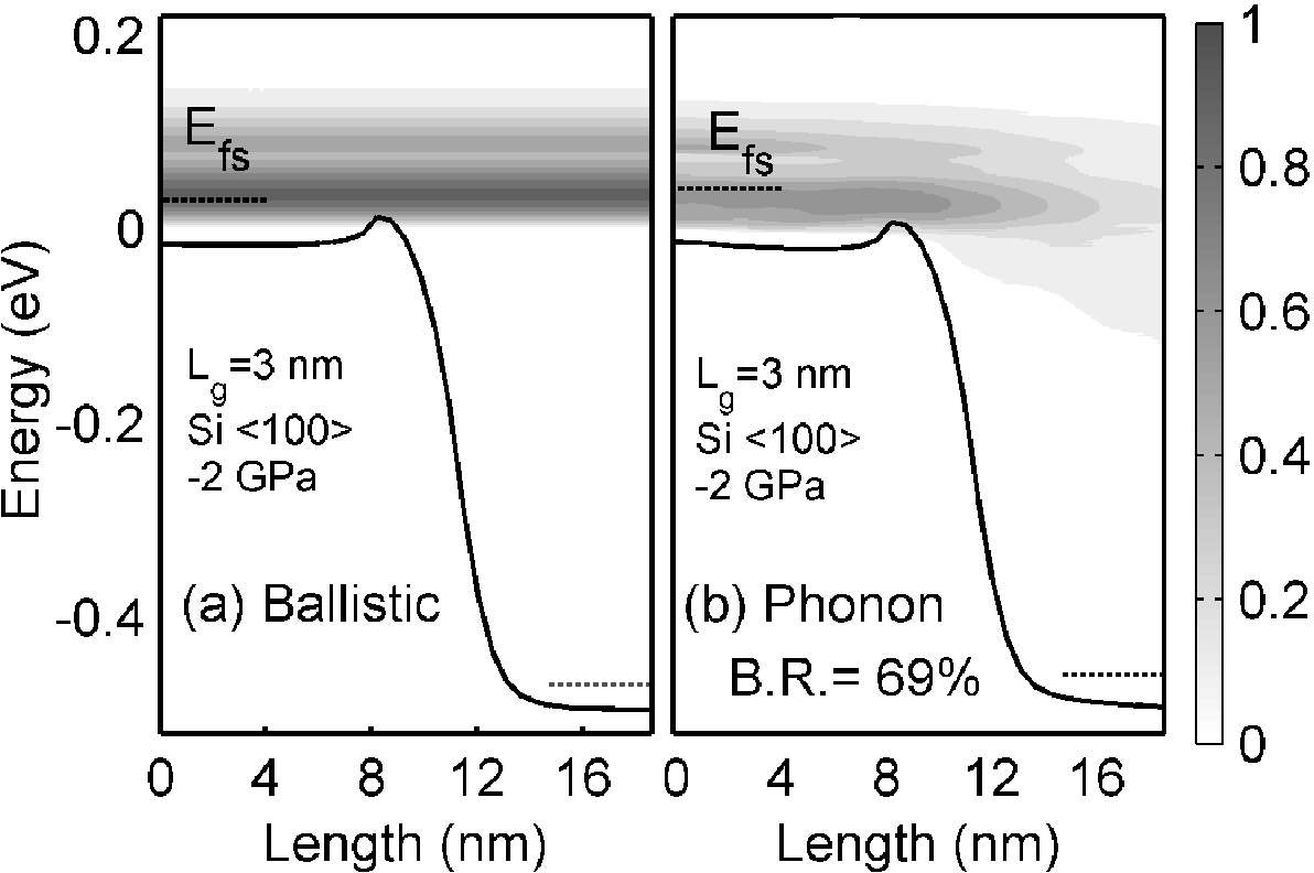
After computing the in the ballistic , the ON state current was recalculated in the presence of electron-phonon scattering [15]. The ON state current limited by electron-phonon scattering was computed for Si100 under the condition of no-stress and a compressive uniaxial stress of -2GPa. It should be noted Si100 are also the best performing nanowire cases in the ballistic limit at the different channel lengths. The phonon limited ON current for InAs is assumed to be of the ballistic ON current [16]. Phonon scattering lowers the with Si100 operating at and compressively stresses Si100 operating at of the ballistic limit. It is expected for the compressively stressed Si100 to have a lower ballisticity ratio because of increased density of states for scattering owing to its heavier CB minima mass. However, with reducing channel length the ballistic ratio (B.R.) improve as the distance over which a carrier can back-scatter reduces [17]. At nm, begins to operate at while compressively stresses Si100 operates at nearly of the ballistic limit (Fig 6(c)).
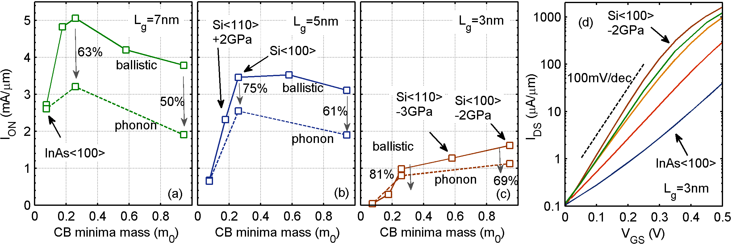
Interestingly, InAs 100, which is currently an actively researched material for future MOSFET scaling, and the tensiled strained Si 110, which is the current industry standard, both lag behind in performance at 8 nm. This is a critical understanding that as the channel lengths scale below 8 nm we enter a new regime of device operation where the device performance is severely limited by S-D tunneling. However, at the same time engineering a relatively heavier transport mass can still lead to performance improvements. It is still encouraging to see that the compressively stressed Si100 nanowire with the channel length scaled to 3 nm, even in presence of phonon scattering, is still able to deliver a respectable at supply voltage of (Fig. 7).
Although, the ON state currents are shown to reduce with channel lengths, the design solution to scaling MOSFETs at 8 nm could lie in vertically stacked multiple nanowire MOSFETs that increases the final without compromising on subthreshold characteristics [18].
V Conclusion
In this work the deleterious effects of S-D tunneling in nanowire n-MOSFETs at 8 nm are highlighted in realistically gated and extended devices. Since S-D tunneling depends on the transport mass, as a first step the different CB minima masses that can be engineered in Si and InAs are shown. Next, using full-band quantum simulations based on tight-binding model the subthreshold and ON state performances are analyzed. The monotonic improvement in subthreshold slope with heavier CB minima mass is clearly observed as a heavy mass limits S-D tunneling. At the same time the ON state performance does not improve monotonically but shows a peak-like nature. This is due to the tradeoff condition that a heavy (or light) mass offers in terms of OFF-state and ON-state properties. The present results show that the optimal device performance at 8 nm lie in heavier () transport mass channel designs. A realistic scenario of scaling MOSFETs well below 8 nm could lie in channel designs with a heavy transport mass to improve sub-threshold characteristics and multiple vertically stacked nanowires to boost the ON state current.
Acknowledgment
The authors would like to thank Materials, Structures and Devices Focus Center, which is one of the six research centers funded under the Focus Center Research Program (a Semiconductor Research Corporation entity); nanoHUB for the computational resources; and Rosen Center for Advanced Computing, National Institute for Computational Sciences, National Center for Computational Sciences and Texas Advanced Computing Center for the supercomputer resources.
References
- [1] C. Auth, C. Allen, A. Blattner, D. Bergstrom, M. Brazier, M. Bost, M. Buehler, V. Chikarmane, T. Ghani, T. Glassman, R. Grover, W. Han, D. Hanken, M. Hattendorf, P. Hentges, R. Heussner, J. Hicks, D. Ingerly, P. Jain, S. Jaloviar, R. James, D. Jones, J. Jopling, S. Joshi, C. Kenyon, H. Liu, R. McFadden, B. McIntyre, J. Neirynck, C. Parker, L. Pipes, I. Post, S. Pradhan, M. Prince, S. Ramey, T. Reynolds, J. Roesler, J. Sandford, J. Seiple, P. Smith, C. Thomas, D. Towner, T. Troeger, C. Weber, P. Yashar, K. Zawadzki, and K. Mistry, “A 22nm high performance and low-power cmos technology featuring fully-depleted tri-gate transistors, self-aligned contacts and high density mim capacitors,” in VLSI Technology (VLSIT), 2012 Symposium on, june 2012, pp. 131 –132.
- [2] “http://www.itrs.net/links/2011itrs/home2011.htm,” [Online; accessed 10-April-2012].
- [3] M. Luisier, M. Lundstrom, D. Antoniadis, and J. Bokor, “Ultimate device scaling: Intrinsic performance comparisons of carbon-based, InGaAs, and Si field-effect transistors for 5 nm gate length,” in Electron Devices Meeting (IEDM), 2011 IEEE International, dec. 2011, pp. 11.2.1 –11.2.4.
- [4] J. Wang and M. Lundstrom, “Does source-to-drain tunneling limit the ultimate scaling of MOSFETs?” in Electron Devices Meeting, 2002. IEDM ’02. International, 2002, pp. 707 – 710.
- [5] J. Appenzeller, J. Knoch, M. Bjork, H. Riel, H. Schmid, and W. Riess, “Toward nanowire electronics,” Electron Devices, IEEE Transactions on, vol. 55, no. 11, pp. 2827 –2845, nov. 2008.
- [6] J. A. del Alamo, “Nanometre-scale electronics with III-V compound semiconductors,” vol. 479, November 2011, p. 317–323.
- [7] M. Fischetti, L. Wangt, B. Yut, C. Sachs, P. Asbeck, Y. Taur, and M. Rodwell, “Simulation of electron transport in high-mobility mosfets: Density of states bottleneck and source starvation,” in Electron Devices Meeting, 2007. IEDM 2007. IEEE International. IEEE, 2007, pp. 109–112.
- [8] S. Sylvia, H.-H. Park, M. Khayer, K. Alam, G. Klimeck, and R. Lake, “Material Selection for Minimizing Direct Tunneling in Nanowire Transistors,” Electron Devices, IEEE Transactions on, vol. 59, no. 8, pp. 2064 –2069, aug. 2012.
- [9] T. Yu, R. Wang, R. Huang, J. Chen, J. Zhuge, and Y. Wang, “Investigation of nanowire line-edge roughness in gate-all-around silicon nanowire mosfets,” Electron Devices, IEEE Transactions on, vol. 57, no. 11, pp. 2864 –2871, nov. 2010.
- [10] S. Thompson, G. Sun, Y. S. Choi, and T. Nishida, “Uniaxial-process-induced strained-si: extending the cmos roadmap,” Electron Devices, IEEE Transactions on, vol. 53, no. 5, pp. 1010 – 1020, may 2006.
- [11] M. Luisier, A. Schenk, W. Fichtner, and G. Klimeck, “Atomistic simulation of nanowires in the tight-binding formalism: From boundary conditions to strain calculations,” Physical Review B, vol. 74, no. 20, p. 205323, 2006.
- [12] T. B. Boykin, G. Klimeck, and F. Oyafuso, “Valence band effective-mass expressions in the empirical tight-binding model applied to a Si and Ge parametrization,” Phys. Rev. B, vol. 69, p. 115201, Mar 2004. [Online]. Available: http://link.aps.org/doi/10.1103/PhysRevB.69.115201
- [13] T. B. Boykin, G. Klimeck, R. C. Bowen, and F. Oyafuso, “Diagonal parameter shifts due to nearest-neighbor displacements in empirical tight-binding theory,” Phys. Rev. B, vol. 66, p. 125207, Sep 2002. [Online]. Available: http://link.aps.org/doi/10.1103/PhysRevB.66.125207
- [14] T. B. Boykin, M. Luisier, M. Salmani-Jelodar, and G. Klimeck, “Strain-induced, off-diagonal, same-atom parameters in empirical tight-binding theory suitable for [110] uniaxial strain applied to a silicon parametrization,” Phys. Rev. B, vol. 81, p. 125202, Mar 2010. [Online]. Available: http://link.aps.org/doi/10.1103/PhysRevB.81.125202
- [15] M. Luisier and G. Klimeck, “Atomistic full-band simulations of silicon nanowire transistors: Effects of electron-phonon scattering,” Physical Review B, vol. 80, no. 15, p. 155430, 2009.
- [16] M. Luisier and G. Klimeck, “Phonon-limited mobility and injection velocity in n-and p-doped ultrascaled nanowire field-effect transistors with different crystal orientations,” in Electron Devices Meeting (IEDM), 2010 IEEE International. IEEE, 2010, pp. 8–6.
- [17] C. Jeong, D. Antoniadis, and M. Lundstrom, “On backscattering and mobility in nanoscale silicon mosfets,” Electron Devices, IEEE Transactions on, vol. 56, no. 11, pp. 2762 –2769, nov. 2009.
- [18] E. Bernard, T. Ernst, B. Guillaumot, N. Vulliet, P. Coronel, T. Skotnicki, S. Deleonibus, and O. Faynot, “Multi-channel field-effect transistor (mcfet) -part i: Electrical performance and current gain analysis,” Electron Devices, IEEE Transactions on, vol. 56, no. 6, pp. 1243 –1251, june 2009.