Graphene Optical properties of low-dimensional, mesoscopic, and nanoscale materials and structures Infrared and Raman spectra
Enhancing the absorption of graphene in the terahertz range
Abstract
We study graphene on a photonic crystal operating in the terahertz (THz) spectral range. We show that the absorption of graphene becomes a modulated function of frequency and can be enhanced by more than three times at specific frequency values, depending on the parameters of the system. The problem of a semi-infinite photonic crystal is also solved.
pacs:
81.05.uepacs:
78.67.-npacs:
78.30.-jThe optical properties of graphene have been extensively studied both theoretically [1, 2, 3, 4, 5, 6, 7, 8, 9, 10, 11, 12, 13, 14] and experimentally [15, 16, 17, 18, 19, 20, 21, 22]. More recently, the interest has shifted to how graphene interacts with electromagnetic radiation in the THz spectral range [23, 24, 25, 26, 27, 28]. In particular, one of the goals is to enhance the absorption of graphene. This maybe done in different ways: (i) producing micro-disks of graphene on a layered structure [23]; (ii) exploiting the physics of quantum dots on graphene [25]; (iii) using a graphene based grating [29, 30]; (iv) putting graphene inside an optical cavity [31, 32]; and (v) depositing graphene on a photonic crystal, operating in the visible range of the spectrum [14]. In cases (i), (ii), and (iii) the excitation of plasmons is responsible for the enhancement of the absorption. In case (iv) the radiation performs many round trips inside the cavity enhancing the chances of being absorbed by graphene. In case (v) the authors use a photonic crystal made of SiO2/Si. In the visible range of the spectrum the dielectric constants of SiO2 and Si differ by more than one order of magnitude and choosing the width of the SiO2/Si appropriately it is possible to induce a large photonic band gap in the visible range. Combining the presence of the band gap with an initial spacer layer the absorption can be enhanced by a factor of four. In the case studied in Ref. [14] the optical conductivity of graphene is controlled by inter-band transitions. In this regime, the conductivity is frequency independent and reads[15]
| (1) |
a value dubbed the universal conductivity of graphene.
In general, the conductivity of graphene is a sum of two contributions: (i) a Drude term, describing intra-band processes and (ii) a term describing inter-band transitions. At zero temperature the optical conductivity has a simple analytical expression [1, 2, 9, 10, 5]. For what concerns our study, the physics of the system is dominated by the Drude contribution, which reads
| (2) |
where is the relaxation rate, is the Fermi level position with respect to the Dirac point, and is the frequency of the incoming radiation. It should be noted that has a strong frequency dependence and is responsible for the optical behaviour of graphene in the THz spectral range.
In what follows, the absorption of graphene on a system such as the one represented in Fig. 1 is computed. The micro-structure has a first layer (spacer) of SiO2, of length , followed by a periodic array of Si/SiO2 which extends for several layers. We have found that no more than few layers are necessary for obtaining an enhancement of the absorption. We write as
| (3) |
where is a numerical parameter chosen to optimize the absorption, is the dielectric constant of the spacer (SiO2), and is a parameter of the order of few microns also chosen to optimize the absorption. The lengths of the Si/SiO2 periodic structure layers are given by
| (4) |
where , with () standing for the dielectric constant of Si(SiO2). In the THz we approximate the dielectric constants of Si and SiO2 by their static values, and .
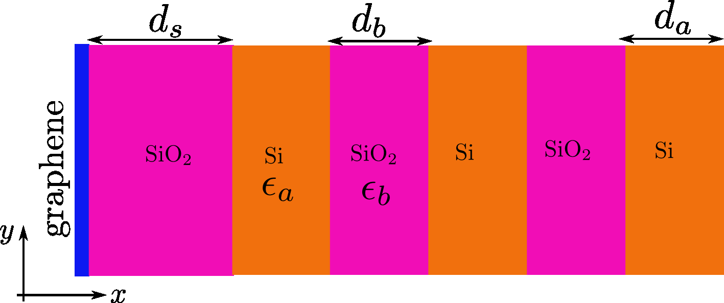
To determine the absorption we have to compute the amount of light reflected and transmitted by and through the structure, respectively. If we denote the transmittance by and the reflectance by , the absorbance is defined, assuming normal incidence, as
| (5) |
It is also assumed that the radiation impinges from the air and emerges the structure to the air as well. Since we are considering normal incidence, no distinction is necessary between and polarized waves.
An electromagnetic wave impinges on graphene from the left along the direction. Due to reflection on the structure the electric field has the form
| (6) |
From Maxwell’s equations, the magnetic field is given by
| (7) |
At the graphene interface the boundary conditions are and , where the subscript () stands for the fields to the left(right) of graphene. At the other interfaces the boundary condition for the magnetic field is simply . On the right hand side of the structure we write the electric field as
| (8) |
Using the transfer matrix method we can relate the fields on the left of the structure to the fields on the right as
| (9) |
from where it follows
| (10) |
and
| (11) |
For the structure we are considering, the transfer matrix is given by
| (12) |
where is the number of times the matrix is repeated in the structure and reads
| (13) |
The several matrices appearing in and are given below. The matrix characterizing the free propagation through a given material is
| (14) |
with . The matrix referring to the transfer through the boundary of two dielectrics is given by
| (15) |
In particular, and refers to the passage from the air to the last slab of Si and from the first SiO2 spacer to the air, respectively [thus in Eq. (15)]. The matrix characterizes the transfer through graphene to air. Here matrix
| (16) |
is the fine structure constant and is a dimensionless function defined by
| (17) |
We note that in the infinite structure we can apply Bloch theorem, and relate the electric field amplitudes in the unit cell with those in the unit cell using the transfer matrix as
| (18) |
where is the Bloch wave vector. Then the spectrum of the infinite structure can be obtained from the condition (here is the unit matrix). Using the property of transfer matrix , we obtain that the spectrum of the infinite photonic crystal,
| (19) |
is defined by trace of only. From Eq. (19) the photonic band gaps can be obtained with no difficulty. We can also access the photonic band gaps by transmittance calculations, a route we choose below.
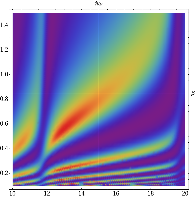
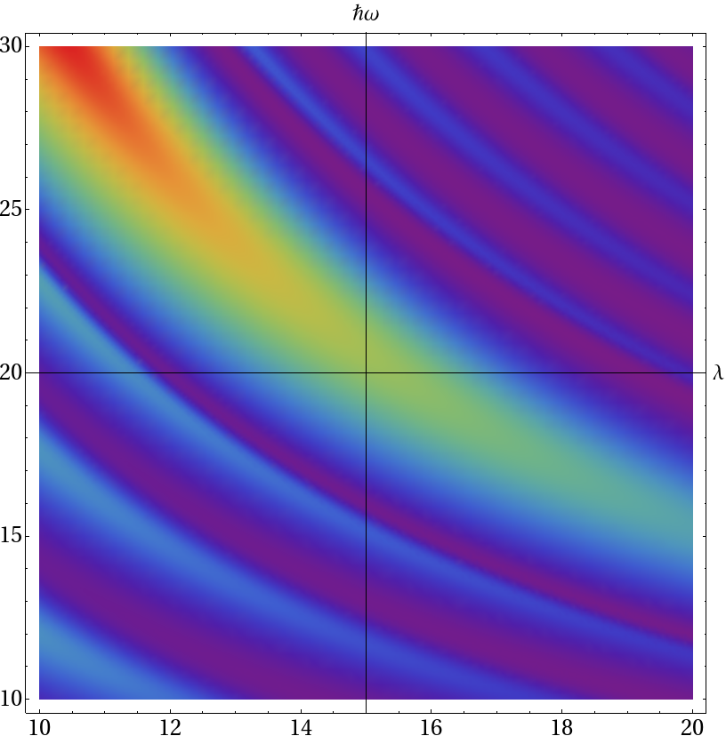
In Fig. 2 we represent the absorbance as function of: (i) the parameter and the photon energy (in meV)[top panel]; (ii) the parameter (in m) and [bottom panel]. Recall that the parameter controls the length of the SiO2 spacer whereas influences the length of the layers constituting the periodic structure. The high-intensity spots correspond to regions in parameters space where the absorbance is higher. The axes in Fig. 2 intercept at one of those high intensity spots. The width of the high intensity regions along the direction gives the width of the resonance. The position of the high-intensity regions is sensitive to the parameter , as can be seen in the bottom panel of Fig. 2. These type of plots allow the optimization of the structure in order to maximize the absorbance. An optimized absorbance peak is given in Fig. 3. The parameters chosen are those corresponding to the interception of the horizontal and vertical lines in Fig. 2. In Fig. 3 we represent the absorbance, the reflectance, and the transmittance as function of the frequency of the incoming photon. Since the dielectric constants we have used for SiO2 and Si are real, all the absorption comes of graphene alone. The intricate behaviour seen on the reflectance and transmittance curves, on the other hand, is mainly due to the structure on the right hand side of graphene. The dashed lines in the same figure represent the behaviour of free standing graphene.
Several aspects are worth mention. Although we have used a fairly small value of , a stop gap due to the photonic band gap of the infinite crystal is already apparent. This happens because the difference between the dielectric constants of SiO2 and Si is significant. Most important however is the enhancement of the absorbance near the center of the photonic band gap. We see that around an energy meV the absorbance is almost four times larger than the absorbance of free standing graphene (assuming it can be doped some how, e. g., by chemical doping [33, 34]; if we had chosen graphene on a SiO2 wafer of the size of the photonic crystal the absorbance would be smaller than that for the free standing case). If we had chosen somewhat different parameters the resonance would shift to the edges of the stop gap. In the absorbance panel we plot the cases , , and . As it can be seen, for the absorbance is not as intense as in the other two cases. At the same time the main difference is the appearance of new satellite peaks to the left and to the right of the main one when we change from to , and to . The nature of these peaks can be expressed in the following simplified manner. In the infinite periodic structure allowed bands are continuous functions of Bloch wave vector , while in the periodic structure containing a finite number of periods the effect of quantization takes place: allowed bands consist of the discrete set of the frequencies, which can be determined from Eq.(19) using the discrete Bloch vectors for (see Ref. [35]). In particular, for the mode with correspond to frequencies meV and meV (here we take into account the frequency range of Fig.3 only), while for the allowed frequencies are meV (mode with ), meV, and meV (mode with ). In both cases the predicted frequencies correspond well with the absorption peaks below and above the stop gap seen in Fig.3.
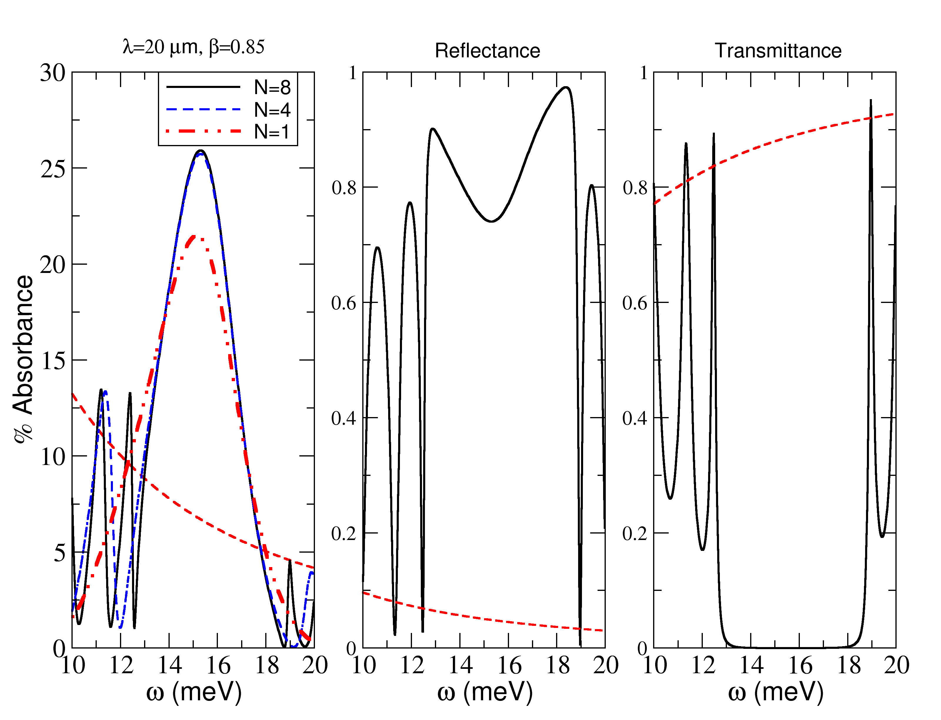
It is instructive to compute the absorbance, reflectance, and transmittance when the photonic crystal is semi-infinite. In this case the oscillations due to the finiteness of the crystal seen in Fig. 3 are absent and it is possible to derive simple analytical formulae for the above quantities. From Eq.(18) it follows that
| (20) |
where are the matrix elements of the matrix . Now the amplitudes for relate to the amplitudes in the first Si slab as
| (25) | |||||
| (30) |
from which it follows that
| (31) | |||
| (32) |
leading to the reflectance amplitude
| (33) |
from which the reflectance is computed as . Because in each slab there is always an incoming and an outgoing wave the calculation of the transmittance is less obvious. We have to compute two field ratios:
| (34) |
and
| (35) |
Then, the transmittance is given by
| (36) |
where the factor comes from the calculation of the flux. In Fig. 4 we plot the absorbance (left), reflectance (center), and transmittance (right) as function of frequency for a semi-infinite photonic crystal. The resonance in the absorbance coincides exactly with that seen in Fig. 3, but the oscillations also seen in Fig. 3 are not present here.
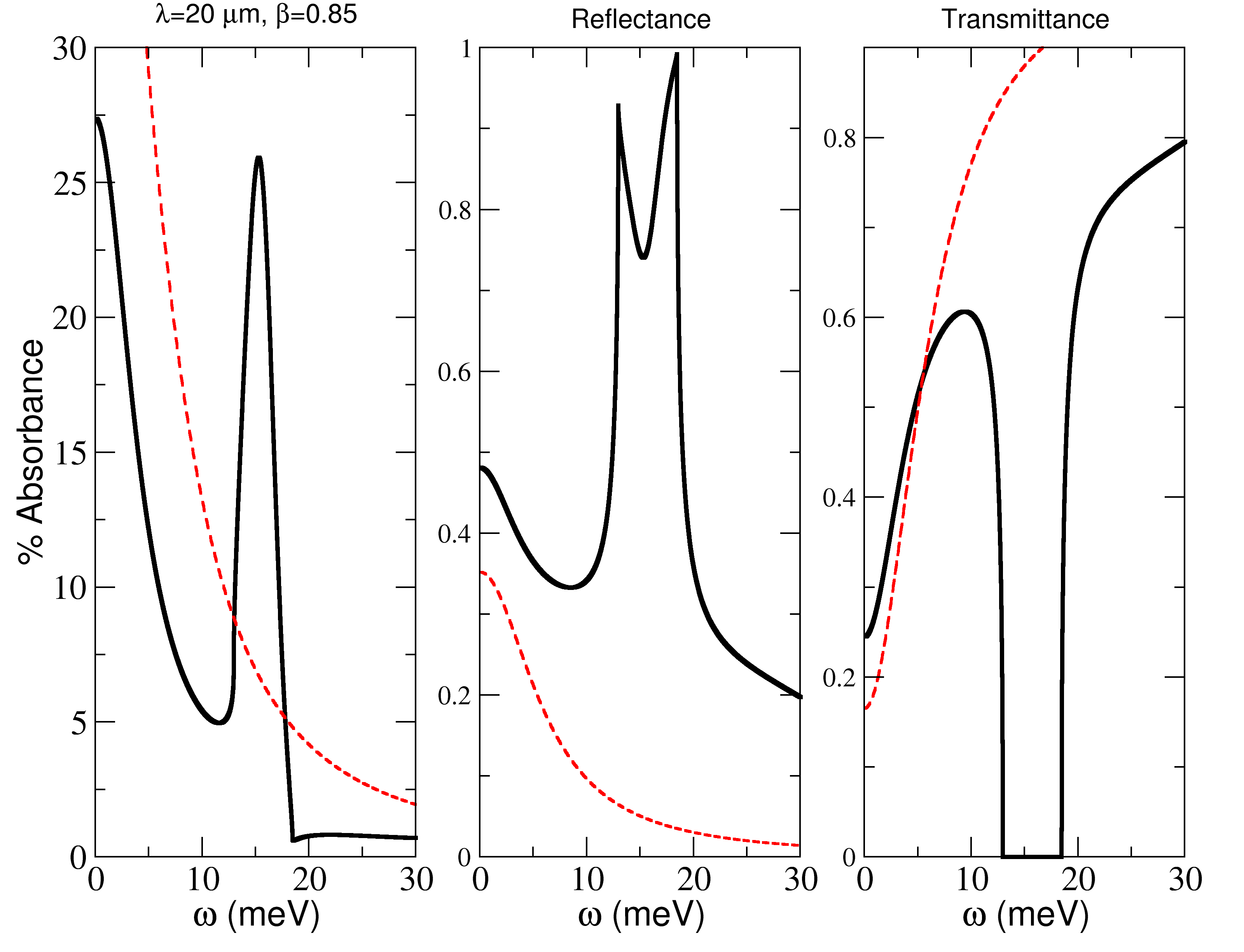
In conclusion, it is possible to use a photonic crystal-like structure to enhance the absorption of radiation by graphene in the THz spectral range at specific frequencies. The effect depends on the geometric properties of the crystal. At the center of the photonic band gap the absorption increases at the expenses of the reflectance (the resonance can shift its position depending on the parameters chosen). If the Fermi energy increases so does the absorption and the width of the peak. It is also clear that for a finite crystal the absorbance becomes a modulated function of frequency. We have chosen the widths of the SiO2 and Si having the same dependence on (exception made to the initial layer which has the extra parameter ). If we had chosen them to be different we would have an extra degree of freedom to tweak the absorbance curves, but the optimization procedure would become cumbersome. If we had sandwiched graphene between two dielectrics the absorbance would decrease because of the optical conductivity would appear in the equations divided by the square root of the dielectric constant of the medium. For the parameters of Fig. 3 the next stop gap appears at an energy of about 47 meV (not shown). There the enhancement of the absorbance is larger by a factor of four relatively to the free standing case. Finally we note that the device does not necessarily require a gate for doping graphene. Stable hole doping by chemical methods have recently been achieved, without affecting the transparency of the material [33].
References
- [1] Peres N M R, Guinea F and Castro Neto A H 2006 Phys. Rev. B 73 125411
- [2] Falkovsky L A and Pershoguba S S 2007 Phys. Rev. B 76 153410
- [3] Stauber T, Peres N M R and Guinea F 2007 Phys. Rev. B 76 205423
- [4] Stauber T, Peres N M R and Castro Neto A H 2008 Phys. Rev. B 78 085418
- [5] Stauber T, Peres N M R and Geim A K 2008 Phys. Rev. B 78 085432
- [6] Gusynin V P, Sharapov S G and Carbotte J P 2009 New J. Phys. 11 095013
- [7] Grushin A G, Valenzuela B and Vozmediano M A H 2009 Phys. Rev. B 80 155417
- [8] Mishchenko E G 2009 Phys. Rev. Lett. 103 246802
- [9] Castro Neto A H, Guinea F, Peres N M R, Novoselov K S and Geim A K 2009 Rev. Mod. Phys. 81 109
- [10] Peres N M R 2010 Rev. Mod. Phys. 82 2673
- [11] Yang L, Deslippe J, Park C H, Cohen M L and Louie S G 2009 Phys. Rev. Lett. 103 186802
- [12] Peres N M R, Ribeiro R M and Castro Neto A H 2010 Phys. Rev. Lett. 105 055501
- [13] Ferreira A, Viana-Gomes J, Bludov Y V, Pereira V M, Peres N M R and Castro Neto A H 2011 Phys. Rev. B 84 235410
- [14] Liu J T, Liu N H, Li J, Li X J and Huang J H 2012 Appl. Phys. Lett. 101 052104
- [15] Nair R R, Blake P, Grigorenko A N, Novoselov K S, Booth T J, Stauber T, Peres N M R and Geim A 2008 Science 320 1308
- [16] Kuzmenko A B, van Heumen E, Carbone F and van der Marel D 2008 Phys. Rev. Lett. 100 117401
- [17] Mak K F, Sfeir M Y, Wu Y, Lui C H, Misewich J A and Heinz T F 2008 Phys. Rev. Lett. 101 196405
- [18] Li Z Q, Henriksen E, Jiang Z, Hao Z, Martin M C, Kim P, Stormer H and Basov D 2008 Nature Phys. 4 532
- [19] Wang F, Zhang Y, Tian C, Girit C, Zettl A, Crommie M and Shen Y R 2008 Science 320 206
- [20] Kuzmenko A B, Crassee I, van der Marel D, Blake P and Novoselov K S 2009 Phys. Rev. B 80 165406
- [21] Crassee I, Levallois J, Walter A L, Ostler M, Bostwick A, Rotenberg E, Seyller T, van der Marel D and Kuzmenko A B 2011 Nat. Phys. 7 48
- [22] Bao Q, Zhang H, Wang B, Ni Z, Lim C H Y X, Wang Y, Tang D Y and Loh K P 2011 Nature Photonics 5 411
- [23] Yan H, Li X, Chandra B, Tulevski G, Wu Y, Freitag M, Zhu W, Avouris P and Xia F 2012 Nature Nano. 7 330
- [24] Chen J, Badioli M, Alonso-Gonzalez P, Thongrattanasiri S, Huth F, Osmond J, Spasenovic M, Centeno A, Pesquera A, Godignon P, Zurutuza A, Camara N, de Abajo J G, Hillenbrand R and Koppens F 2012 Nature 487 77
- [25] Konstantatos G, Badioli M, Gaudreau L, Osmond J, Bernechea M, de Arquer P G, Gatti F and Koppens F H L 2012 Nature Nanotechnology 7 363
- [26] Fei Z, Andreev G O, Bao W, Zhang L M, McLeod A S, Wang C, Stewart M K, Zhao Z, Dominguez G, Thiemens M, Fogler M M, Tauber M J, Castro Neto A H, Lau C N, Keilmann F and Basov D N 2011 Nano Lett. 11 4701
- [27] Fei Z, Rodin A S, Andreev G O, Bao W, McLeod A S, Wagner M, Zhang L M, Zhao Z, Dominguez G, Thiemens M, Fogler M M, Castro Neto A H, Lau C N, Keilmann F and Basov D N 2012 Nature 487 82
- [28] Vicarelli L, Vitiello M S, Coquillat D, Lombardo A, Ferrari A C, Knap W, Polini M, Pellegrini V and Tredicucci A 2012 Nature Materials 11 865
- [29] Peres N M R, Ferreira A, Bludov Y V and Vasilevskiy M I 2012 J. Phys.: Condens. Matter 24 245303
- [30] Bludov Y V, Peres N M R and Vasilevskiy M I 2012 Phys. Rev. B 85 245409
- [31] Ferreira A, Peres N M R, Ribeiro R M and Stauber T 2012 Phys. Rev. B 85 115438
- [32] Furchi M, Urich A, Pospischil A, Lilley G, Unterrainer K, Detz H, Klang P, Andrews A M, Schrenk W, Strasser G and Mueller T 2012 Nano Letters 12 2773
- [33] Tongay S, Berke K, Lemaitre M, Nasrollahi Z, Tanner D B, Hebard1 A F and Appleton B R 2011 Nanotechnology 22 425701
- [34] Liu H, Liu Y and Zhu D 2011 J. Mater. Chem. 21 3335
- [35] Bludov Y V and Konotop V V 2007 Phys. Rev. E 76 046604