Probing the local density of states in three dimensions with a scanning single quantum emitter
Abstract
Their intrinsic properties render single quantum systems as ideal tools for quantum enhanced sensing and microscopy. As an additional benefit, their size is typically on an atomic scale which enables sensing with very high spatial resolution. Here, we report on utilizing a single nitrogen vacancy center in nanodiamond for performing three-dimensional scanning-probe fluorescence lifetime imaging microscopy. By measuring changes of the single emitter’s lifetime information on the local density of optical states is acquired at the nanoscale. This technique to gather information on the local density of optical states is important for the understanding of fundamental quantum optical processes as well as for the engineering of novel photonic and plasmonic devices.
Quantum-enhanced sensing has become one of the major fields in quantum technology O’Brien, Furusawa, and Vuckovic (2009). The quantum properties, on the one hand, allow for measuring with a precision overcoming the classical limit Jaekel and Reynaud (1990). On the other hand, single quantum systems represent ideal sensing probes. Their unique properties do not necessarily utilize intrinsic quantum effects, but rather the fact that quantum systems are typically very small. Therefore, they can probe the rather large local fields of single atoms or a local environment consisting of only a few molecules. Optical quantum probes provide the additional advantage of reliable initialization as well as efficient and easy read-out. In this paper we report for the first time on utilizing a single quantum emitter (QE) for performing three-dimensional scanning-probe fluorescence lifetime imaging microscopy (FLIM) introducing the technique of QE-FLIM.
First optical scanning quantum probes have appeared more than 10 years ago Michaelis et al. (2000); Guthohrlein et al. (2001) in fluorescence microscopy. By now, recent advances with respect to the stability of solid-state emitters have paved the way for several novel approaches where quantum emitter scanning probes are used to detect electric Dolde et al. (2011) or magnetic fields Maze et al. (2008). It is also possible to detect vacuum fields via modifications of the spontaneous lifetime of an emitter, since it is known from quantum optics that the spontaneous emission is not an intrinsic property of an emitter, but is determined by the local density of states (LDOS). More generally speaking, any light-matter coupling, as described on the fundamental level by a single dipole coupled to modes of the electromagnetic field, can be modified by changing the LDOS Mazzei et al. (2007). By carefully designing the LDOS, it is possible to significantly enhance the functionality of devices in photonics and plasmonics. Examples are spontaneous emission control for fast optical modulators Englund et al. (2009), for energy-efficient lasing Fujita et al. (2005), or for improving light trapping in solar cells Callahan, Munday, and Atwater (2012). The design of the LDOS is particularly crucial for fundamental few-photon devices in quantum optical engineering, e.g. for efficient and fast single photon sources needed in optical quantum computing O’Brien (2007). Photonic structures such as microcavities Vahala (2003), optical antennas Novotny and van Hulst (2011), and photonic metamaterials Cortes et al. (2012) allow for a design of the LDOS in all three spatial dimensions. Therefore, techniques to obtain precise information about the LDOS on the nanoscale are crucial. There exist several approaches to gain this information, e.g. coating of the structures of interest with fluorescent dyes Hoogenboom et al. (2009), mapping with scanning near field microscopes Imura, Nagahara, and Okamoto (2005); De Wilde et al. (2006), nanopositioning of defect centers Schell et al. (2011a); Wolters et al. (2012) or colloidal quantum dots Ropp et al. (2013), or employing a scanning electron microscope Sapienza et al. (2012). Fluorescent probes indicate the LDOS via the observed lifetime changes, with most previous probes utilizing large ensembles of emitters like molecules in nanobeads Frimmer, Chen, and Koenderink (2011). However, because of averaging over an ensemble with different spatial positions and electromagnetic environments, the excitation decay curve is multi-exponential. This makes it difficult to quantify modifications of the decay dynamics when scanning the probe. Additionally, the ultimate spatial resolution is still given by the diameter of the doped beads.
A fundamental FLIM probe would consist of a single atom, and indeed two groups have shown the capability of single trapped ions to map the LDOS Guthohrlein et al. (2001); Kreuter et al. (2004). However, single ions in an ultra-high vacuum environment do not meet the requirement for a robust scanning-probe where a point-like fluorescent dipole is located at a scanning-tip, which can be actively stabilized and scanned across an arbitrary substrate. Defect centers in nanodiamonds Kurtsiefer et al. (2000); Jelezko and Wrachtrup (2006) provide optimum properties for this purpose, since they are optically stable even at room temperature. Their optical stability even allows for trapping with optical tweezers Horowitz et al. (2012); Geiselmann et al. (2013). Here, we use a single-photon emitting NV center as a scanning probe for fluorescence lifetime imaging. The single emitter nature of the NV center leads to an increase in obtainable resolution, only limited by the size of a single NV center and the mechanical stability of the microscope. With only one emitter participating, there is no temporal broadening due to lifetime variations between different emitters in an ensemble. Furthermore we introduce a novel mapping technique to gather three-dimensional (3D) lifetime information while keeping the orientation of the probe fixed. The power of this approach is demonstrated by mapping the local density of states in the vicinity of silver nanowires Ditlbacher et al. (2005).
Results
The experimental setup is a confocal microscope combined with an atomic force microscope for simultaneous measurements (see Methods and Figure 5 for details). A very important task in quantitative QE-FLIM is the characterization of the probe. It has to be a single emitter with known properties such as orientation, lifetime, and quantum efficiency. To prove the single emitter character, measurements of the autocorrelation function are performed before and after the nanodiamonds (typical sizes ca. ) are attached to the tip (see Figure 1 (a,b)). A indicates that the main photon contribution is from a single emitter Loudon (2000). Only in this way averaging over several emitters with slightly different lifetimes and slightly different positions can be excluded and smearing out the measurement signal is avoided.
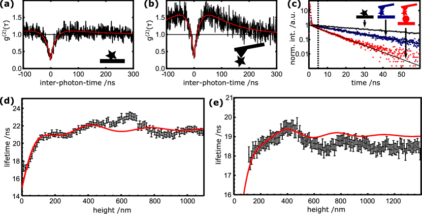
A change in the bunching behavior when comparing Figures 1(a) and (b) is attributed to a changed dielectric as well as a changed chemical environment, which can influence the charge of the NV center Jelezko and Wrachtrup (2006); Rondin et al. (2010); Hauf et al. (2011). The lifetime can be extracted from Figure 1(c). It shows a mono-exponential decay curve of the NV center’s excited state for different situations: black for the nanodiamons on a coverslip ( ns), blue for the nanodiamond glued to the tip far from the surface ( ns), and red with the tip close to a silver nanowire ( ns). After the nanodiamond is glued to the tip, the lifetime only varies when the environment, and therefore the LDOS, changes, e.g. when approaching a silver nanowire (red curve in Figure 1(c)). Figure 1 (d,e) show detailed data of nanodiamond probes approaching a glass surface. When the emitter approaches the surface an oscillatory behavior is visible as predicted by the theory for a dipole over a surface Lukosz and Kunz (1977). Deviations can be explained by the fact that the silicon AFM tip gives rise to an additional surface not covered by the theory given in Reference Lukosz and Kunz (1977). From the theoretical curves the NV center’s orientation, its position within the nanodiamond, as well as the quantum efficiency of its optical transition can be derived in principle (see Supplementary Information).
With a pre-characterized and scanable single quantum emitter, the LDOS can now be mapped on the nanoscale in all three spatial dimensions with high resolution. In order to do this, for each position of a scanned area the detected photons are sorted with respect to the actual height of the oscillating cantilever (see Methods). In this way the three dimensional quantum emitter fluorescent lifetime microscopy (QE-FLIM) is established.
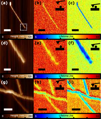
A first example is shown in Figure 2, where silver nanowires of approximately in diameter are raster-scanned by QE-FLIM. Figure 2(a,d,g) are AFM topography scans showing a wire, a zoom at the wire’s end, and a wire network, respectively. In Figure 2(b,e,h) and (c,f,i) lifetimes images are shown for the emitter being in the distant quarter of its oscillation and in the quarter close to the surface. The emitter’s lifetime decreases close to the surface, as it is expected due to the higher index of refraction and therefore higher LDOS Lukosz and Kunz (1977). Close to the nanowire the additional plasmonic modes account for an even more reduced lifetime. Sharp features of the image of the nanowire observed when the emitter is close to the surface blur out when the emitter is distant. In Figure 2(g-i) a network of crossed wires is scanned with the QE-FLIM. Here, the cantilever’s oscillation amplitude was set twice as large as in Figure 2(a-f). When scanning along the nearly horizontal wire the expected decrease of the emitter’s lifetime is observed, but also an increase in lifetime is found in a scan parallel to it. An explanation for this behavior is that the nanodiamond’s position is not exactly at the center of the AFM tip, so that an asymmetry arises. These artifacts can be avoided by taking into account topography information as demonstrated in the following.
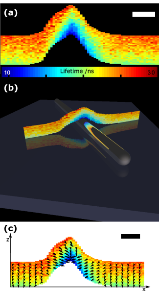
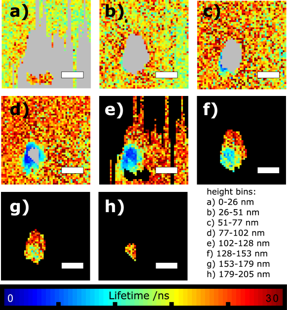
A unique feature of 3D QE-FLIM is the possibility to derive topography corrected lifetime images. Whereas Figure 2 displayed lateral scans for two different relative position of the scanning cantilever, Figure 3 shows a scan crossing a silver nanowire in a plane perpendicular to the sample surface. The amplitude of the cantilever’s oscillation of is divided in 25 height bins. At the same time for each pixel the absolute height of the sample is acquired with the AFM. Therefore Figure 3 represents a lifetime image with completely known spatial coordinates avoiding artifacts which often appear in scanning probe images. This method of topography correction can be applied to any sample. It is apparent how the lifetime decreases when approaching the glass cover slip or the surface of the silver wire. The observed rate enhancement lies well in the order expected from previous experiments dealing with the coupling of nanodiamonds to silver nanowires Huck et al. (2011). The highest rate enhancement found is a factor of 6.1, when comparing the diamond on the glass cover slip to the diamond coupled to a silver wire and a factor of for 14.5 for a gold nanosphere (see Supplementary Information).
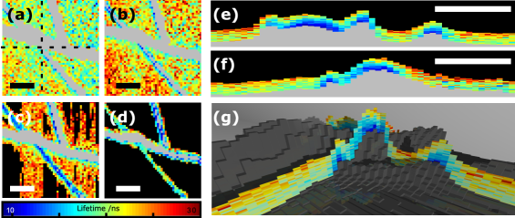
As an additional example Figure 4 shows lateral slices parallel to the sample with silver wires for a specific height as derived from the full 3D data set.
Discussion
From the three-dimensional topography corrected data sets it is possible to derive another important parameter, the gradient of the fluorescence lifetime map. Figure 3(c) shows a gradient QE-FLIM image of a single silver wire. It is apparent that the gradient indicates the position of nanometer-sized objects which modify the LDOS. This may be used to localize such objects even in topography-free sample, e.g., buried semiconductor quantum dots Badolato et al. (2005). As another important feature gradient QE-FLIM provides insight in the coupling mechanism of the quantum emitter probe and the sample. For example as was shown recently Tisler et al. (2013) the lifetime-reduction due to Foerster-coupling depends in a characteristic way on the dimensionality of substrate. Gradient QE-FLIM images can indicate these coupling mechanisms directly and with high spatial resolution.
In conclusion we have introduced a scanning probe microscope employing a single point-like quantum emitter as a probe for the LDOS. This technique avoids broadening of the measurement signal due to multiple emitters at different locations or with different lifetimes. By operation in tapping mode and collecting the photons tagged with the cantilever position, lifetime data in all three dimensions can be acquired in a single scan without topography artifacts. These three dimensional data sets give detailed insight to the electromagnetic environment at the nanoscale with sub-diffraction-limit resolution.
Methods

Confocal microscope The optical microscope in this experiment is a homebuilt sample-scanning inverted confocal microscope (see Figure 5(a)). An objective with a numerical aperture of 1.35 (UPlanSApo60XO, Olympus) is used to excite the NV center and to collect the single photons. Excitation is done with a picosecond laser at a wavelength of with a variable repetition rate (LDH-P-FA-530, Picoquant). A repetition rate of is used when scanning with the QE-FLIM microscope, while a rate of is used for the autocorrelation measurements. Autocorrelation measurements are performed with a Hanbury-Brown and Twiss setup. After spectral filtering avalanche photodiodes (SPCM-AQR-14, Perkin Elmer) are used to detect the single photons.
Atomic force microscope A tip scanning atomic force microscope (NanoWizard II, JPK Instruments) is mounted on the confocal microscope (see Figure 5(a)). The nanodiamonds (MSY 0-0.05 GAF, Microdiamant AG) are spin coated on a cleaned coverslip, pre-characterized using the confocal microscope and subsequently attached to the AFM cantilever. A technique similar to the one described in Reference Schell et al. (2011b) is used to craft the diamonds to the tip. To make the nanodiamonds stick, the cantilevers are dipped in a drop of poly-L-lysine solution Cuche et al. (2009). The typical size of the nanodiamonds glued to the tip is about . Cantilevers are silicon tapping mode cantilevers (NSG03, NT-MDT), which proved to contribute only very little to background fluorescence. While acquiring image data, the nanodiamond which is attached to the cantilever is positioned in the confocal volume of the microscope and the sample is scanned with a sample scanner.
Electronic setup and data processing Photon detection event time tags are recorded using a PicoHarp 300 (Picoquant) data acquisition electronic. Markers for spatial coordinates are also fed to the PicoHarp 300 and are collected within the time tag stream. To extract the 3D lifetime information, in addition to the current scanning position, the cantilever’s oscillation is also fed to the correlation electronics. With that information, the photon detection events at each pixel can be attributed to different height bins (see Figure 5b). Time tags for the cantilevers oscillation are created from the AFM’s modulation reference output using a Schmitt trigger and additional counting electronics, so that only every 4096th period is time tagged. Data in every pixel then is histogrammed with respect to the cantilever height and fitted with a monoexponential decay to calculate the lifetime (see Figure 5(b)). Events in the first are not used in order to avoid artifacts from fast decaying background contributions. The line scan in Figure 3 was averaged over 50 AFM scans to compensate for drift.
Acknowledgements
Support from DFG (FOR1493) is acknowledged.
Author contributions
A.W.S and P.E. performed the measurements and data analysis under the supervision of O.B. A.W.S. conceived the experiment and wrote the manuscript. All authors discussed experiment and manuscript.
References
- O’Brien, Furusawa, and Vuckovic (2009) J. L. O’Brien, A. Furusawa, and J. Vuckovic, Nat. Photon 3, 687 (2009).
- Jaekel and Reynaud (1990) M. T. Jaekel and S. Reynaud, Europhys. Lett. 13, 301 (1990).
- Michaelis et al. (2000) J. Michaelis, C. Hettich, J. Mlynek, and V. Sandoghdar, Nature 405, 325 (2000).
- Guthohrlein et al. (2001) G. R. Guthohrlein, M. Keller, K. Hayasaka, W. Lange, and H. Walther, Nature 414, 49 (2001).
- Dolde et al. (2011) F. Dolde, H. Fedder, M. W. Doherty, T. Nobauer, F. Rempp, G. Balasubramanian, T. Wolf, F. Reinhard, L. C. L. Hollenberg, F. Jelezko, and J. Wrachtrup, Nat Phys 7, 459 (2011).
- Maze et al. (2008) J. R. Maze, P. L. Stanwix, J. S. Hodges, S. Hong, J. M. Taylor, P. Cappellaro, L. Jiang, M. V. G. Dutt, E. Togan, A. S. Zibrov, A. Yacoby, R. L. Walsworth, and M. D. Lukin, Nature 455, 644 (2008).
- Mazzei et al. (2007) A. Mazzei, S. Götzinger, L. de S. Menezes, G. Zumofen, O. Benson, and V. Sandoghdar, Phys. Rev. Lett. 99, 173603 (2007).
- Englund et al. (2009) D. Englund, A. Faraon, A. Majumdar, N. Stoltz, P. Petroff, and J. Vuckovic, Opt. Express 17, 18651 (2009).
- Fujita et al. (2005) M. Fujita, S. Takahashi, Y. Tanaka, T. Asano, and S. Noda, Science 308, 1296 (2005).
- Callahan, Munday, and Atwater (2012) D. M. Callahan, J. N. Munday, and H. A. Atwater, Nano Lett. 12, 214 (2012) .
- O’Brien (2007) J. L. O’Brien, Science 318, 1567 (2007) .
- Vahala (2003) K. J. Vahala, Nature 424, 839 (2003).
- Novotny and van Hulst (2011) L. Novotny and N. van Hulst, Nat. Photon 5, 83 (2011).
- Cortes et al. (2012) C. L. Cortes, W. Newman, S. Molesky, and Z. Jacob, J. Opt. 14, 063001 (2012).
- Hoogenboom et al. (2009) J. P. Hoogenboom, G. Sanchez-Mosteiro, G. Colas des Francs, D. Heinis, G. Legay, A. Dereux, and N. F. van Hulst, , Nano Lett. 9, 1189 (2009).
- Imura, Nagahara, and Okamoto (2005) K. Imura, T. Nagahara, and H. Okamoto, The J. Chem. Phys. 122, 154701 (2005).
- De Wilde et al. (2006) Y. De Wilde, F. Formanek, R. Carminati, B. Gralak, P.-A. Lemoine, K. Joulain, J.-P. Mulet, Y. Chen, and J.-J. Greffet, Nature 444, 740 (2006).
- Schell et al. (2011a) A. W. Schell, G. Kewes, T. Hanke, A. Leitenstorfer, R. Bratschitsch, O. Benson, and T. Aichele, Opt. Express 19, 7914 (2011a).
- Wolters et al. (2012) J. Wolters, G. Kewes, A. W. Schell, N. N sse, M. Schoengen, B. L chel, T. Hanke, R. Bratschitsch, A. Leitenstorfer, T. Aichele, and O. Benson, phys. stat. sol. (b) 249, 918 (2012).
- Ropp et al. (2013) C. Ropp, Z. Cummins, S. Nah, J. T. Fourkas, B. Shapiro, and E. Waks, Nat. Commun. 4, 1447 (2013).
- Sapienza et al. (2012) R. Sapienza, T. Coenen, J. Renger, M. Kuttge, N. F. van Hulst, and A. Polman, Nat. Mater. 11, 781 (2012).
- Frimmer, Chen, and Koenderink (2011) M. Frimmer, Y. Chen, and A. F. Koenderink, Phys. Rev. Lett. 107, 123602 (2011).
- Kreuter et al. (2004) A. Kreuter, C. Becher, G. P. T. Lancaster, A. B. Mundt, C. Russo, H. Häffner, C. Roos, J. Eschner, F. Schmidt-Kaler, and R. Blatt, Phys. Rev. Lett. 92, 203002 (2004).
- Kurtsiefer et al. (2000) C. Kurtsiefer, S. Mayer, P. Zarda, and H. Weinfurter, Phys. Rev. Lett. 85, 290 (2000).
- Jelezko and Wrachtrup (2006) F. Jelezko and J. Wrachtrup, phys. stat. sol. (a) 203, 3207 (2006).
- Horowitz et al. (2012) V. R. Horowitz, B. J. Aleman, D. J. Christle, A. N. Cleland, and D. D. Awschalom, Proc. Natl. Acad. Sci. USA 109, 13493 (2012) .
- Geiselmann et al. (2013) M. Geiselmann, M. L. Juan, J. Renger, J. M. Say, L. J. Brown, F. J. G. de Abajo, F. Koppens, and R. Quidant, Nat. Nano. advance online publication, (2013).
- Ditlbacher et al. (2005) H. Ditlbacher, A. Hohenau, D. Wagner, U. Kreibig, M. Rogers, F. Hofer, F. R. Aussenegg, and J. R. Krenn, Phys. Rev. Lett. 95, 257403 (2005).
- Loudon (2000) R. Loudon, The quantum theory of light., by Loudon, R.. New York, NY (USA): Oxford University Press, 368 p. (Oxford University Press, 2000).
- Lukosz and Kunz (1977) W. Lukosz and R. E. Kunz, J. Opt. Soc. Am. 67, 1607 (1977).
- Rondin et al. (2010) L. Rondin, G. Dantelle, A. Slablab, F. Grosshans, F. Treussart, P. Bergonzo, S. Perruchas, T. Gacoin, M. Chaigneau, H.-C. Chang, V. Jacques, and J.-F. Roch, Phys. Rev. B 82, 115449 (2010).
- Hauf et al. (2011) M. V. Hauf, B. Grotz, B. Naydenov, M. Dankerl, S. Pezzagna, J. Meijer, F. Jelezko, J. Wrachtrup, M. Stutzmann, F. Reinhard, and J. A. Garrido, Phys. Rev. B 83, 081304 (2011).
- Huck et al. (2011) A. Huck, S. Kumar, A. Shakoor, and U. L. Andersen, Phys. Rev. Lett. 106, 096801 (2011).
- Badolato et al. (2005) A. Badolato, K. Hennessy, M. Atatüre, J. Dreiser, E. Hu, P. M. Petroff, and A. Imamoglu, Science 308, 1158 (2005) .
- Tisler et al. (2013) J. Tisler, T. Oeckinghaus, R. St hr, R. Kolesov, F. Reinhard, and J. Wrachtrup, arXiv:1301.0218 (2013).
- Schell et al. (2011b) A. W. Schell, G. Kewes, T. Schröder, J. Wolters, T. Aichele, and O. Benson, Rev. Sci.c Inst. 82, 073709 (2011) .
- Cuche et al. (2009) A. Cuche, A. Drezet, Y. Sonnefraud, O. Faklaris, F. Treussart, J.-F. Roch, and S. Huant, Opt. Express 17, 19969 (2009).
Supplementary Information
I Probe characterization
For lifetime imaging with a single quantum emitter characterization of the probe is crucial. It is not only necessary to prove that the nanodiamond glued to the tip contains indeed only a single NV center, but in addition, its quantum efficiency, position inside the host crystal, and orientation has also to be determined. While it is straightforward to prove single photon emission with a Hanbury-Brown and Twiss setup, it is more difficult to obtain information on quantum efficiency, position, and orientation. We utilize the model of an oscillating single dipole in front of an interface Lukosz and Kunz (1977); Novotny and Hecht (2006) to derive this information. By measuring the NV center’s lifetime at different heights over a coverslip and comparing it to the prediction by the simple model it is possible to calculate its quantum efficiency, position, and orientation.
The theoretical expression for the local density of optical states (LDOS) for a dipole in front of the interface between two media is given by
| (1) |
with
| (2) |
| (3) |
the Fresnel coefficients and
| (4) |
| (5) |
the relations for the wave vectors inside medium
| (6) |
and the abbreviations
The LDOS is dependent on the dipole-interface distance , the wavelength , and the dipole’s orientation . It is assumed that .
To adapt this formula for NV centers, the LDOS for two orthogonal dipoles is added with the assumption, that both dipoles have the same free radiative decay rate. Figure 7a shows two extremal possibilities, both dipoles parallel to the surface and one parallel and one perpendicular. Here, we approximated the broad room temperature spectrum of the NV centers by a Gaussian centered at with a standard deviation of .
The quantum efficiency QE of the NV center can now be calculated according to
| (7) |
| (8) |
The values of the parameters in Equation 1 now can be adjusted to fit the data measured, as shown in Figure 6. The offset in the z axis from the position of the NV center inside the nanodiamond is set to 0, since the quality of the data used and the accuracy of the model is not high enough to estimate values in the order of nanometers.
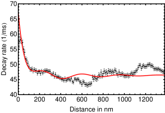
Deviations of data and theory are due to the fact, that the model describes a significantly simplified system - effects arising from the interfaces of the AFM tip are not covered. Nevertheless by modeling the experimental situation in more detail, either analytically or numerically, a better agreement might be achieved. In the following we utilize the simpler model and show the influence of the variation of different parameters.

II QE-FLIM with gold spheres
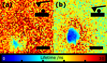
Gold nanospheres are scanned with QE-FLIM. Figure 8 shows a scan over a gold nanosphere of height. The maximum rate enhancement found is a factor of 14.5 when the nanodiamond probe is close to the sphere’s surface.
References
- Lukosz and Kunz (1977) W. Lukosz and R. E. Kunz, J. Opt. Soc. Am. 67, 1607 (1977).
- Novotny and Hecht (2006) L. Novotny and B. Hecht, Principles of Nano-Optics, Principles of Nano-optics (Cambridge University Press, 2006).