One-Dimensional Quantum Channel in Graphene Line Defect
Abstract
Using a tight binding model, we study a line defect in graphene where a bulk energy gap is opened by sublattice symmetry breaking. It is found that sublattice symmetry breaking may induce many configurations that correspond to different band spectra. In particular, a gapless state is observed for a configuration which hold a mirror symmetry with respect to the line defect. We find that this gapless state originates from the line defect and is independent of the width of the graphene ribbon, the location of the line defect, and the potentials in the edges of ribbon. In particular, the gapless state can be controlled by the gate voltage embedded below the line defect. Finally, this result is supported with conductance calculations. This study shows how a quantum channel could be constructed using a line defect and how the quantum channel can be controlled by tuning the gate voltage embedded below the line defect.
pacs:
72.80.Vp, 73.63.-b, 81.07.-b, 81.05.ueI Introduction
Since the experimental discovery of graphene, Novoselov0 ; Novoselov ; Geim1 ; Geim2 extensive attention Avouris ; Neto0 ; Bolotin ; Balandin ; Abergel ; Schwierz has been given to this field due to graphene’s unique band structure and properties. It has been shown in many studies that pristine graphene is a zero-gap semiconductor and has a linear dispersion relationship nearby the Dirac points, Avouris ; Neto0 which makes electrons behave as relativistic Dirac particles. Moreover, it has been experimentally verified that graphene has a remarkably high electron mobility at room temperature, with reported values in excess of . Geim1 High electron mobility makes graphene an excellent conductor. Owing to its exceptional electrical Bolotin and thermal Balandin transport properties, graphene has been an important two-dimensional material for exploring condensed matter physical phenomena Geim1 ; Neto0 ; Abergel and is expected to be very useful in the next generation of electronic devices. Schwierz
Before applications of graphene can be realized in electronic devices, control over the electron transport in graphene needs to be improved. Inspired by the role of defects, vacancies, and dopants in the semiconductor industry, many researchers have studied the effects related to disorder in graphene, which could be due to adsorbed atoms (or molecules), charged impurities, vacancies or other topological defects. Neto0 ; Peres0
Point defects Lusk1 ; Lusk2 ; Carr ; Banhart , and magnetic behavior near point defects, Esquinazi ; Lehtinen ; Vozmediano ; Okada0 ; Yazyev0 ; Wang in graphene have been extensively studied in many papers. Given carbon’s lack of or electrons, magnetism in graphene seems unlikely. Magnetic behavior near point defects has been of increasing interest, and has attracted extensive attention. Cervenka ; Ugeda ; Chang ; Chen In addition, because of universality of grain boundary in graphene, it has been investigated and is predicted to have distinct electronic, Cervenka2 ; Peres ; Yazyev1 ; Mesaros magnetic, Cervenka chemical Malola and mechanical Liu ; Grantab ; Yazyev2 properties that strongly depend on the atomic arrangement. Furthermore, it has also been found that adsorbed atoms (or molecules) greatly affect the properties of graphene, such as lithium, aluminum, iron, and gold adatoms in graphene. Weeks ; HBZhang ; Chan ; Ding The previous researches in this subject illustrate that the properties of graphene can be controlled by defects, grain boundaries, or adsorbed atoms.
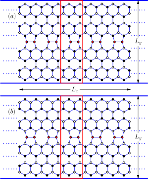
Recently, a peculiar topological line defect in graphene was reported experimentally by Lahiri et al. Lahiri This topological line defect is created by alternating the Stone-Thrower-Wales defect Thrower and divacancies, leading to a pattern of repeating paired pentagons and octagons, as shown in Fig. 1. Importantly, it is found in this experiment that this line defect has metallic characteristics. Subsequently, Gunlycke and White Gunlycke proposed a valley filter based on scattering off this line defect in graphene. Using a tight-binding model calculation, metallic characteristics and Fabry-Perot oscillation phenomena have been observed in graphene line defects by Bahamon et al. Bahamon By using first-principles calculations, researchers from two different groups have calculated the electronic structure of graphene with topological line defects, and predicted a possible ferromagnetic ordering in line defects. Okada ; Kou In addition, a zigzag graphene nanoribbon edge reconstruction with Stone-Wales defects has also been studied recently by Rodrigues et al. Rodrigues
Note that this line defect manifests a metallic behavior in most of reported results. However, because the states of line defect and the bulk states are mixed together in energy, it is difficult to distinguish each other in experiment. In recent, it is reported by a lot of research groups that a energy gap can be generated by various method, e.g. adatoms or substrate. These studies inspire us that the line defect in graphene can be observed directly if the state of line defect falls into the energy gap, and even some promising electronic devices can be fabricated. Motivated by the idea of finding a potential application of line defect, we therefore extend the investigation of line defects in graphene with sublattice symmetry breaking potentials. This paper describes how some novel states are induced in the bulk gap by line defects and that these states can be tuned continuously by changing the gate voltage embedded below the line defect. Based on these results, a quantum channel is proposed at the end of this paper.
The rest of this paper is organized as follows. In Sec. II, the tight-binding Hamiltonian of graphene with a line defect is introduced. Section III gives numerical results along with some discussions. Finally, a brief summary is presented in Sec. IV.
II THEORETICAL MODEL AND FORMULA
In the tight binding approximation with nearest neighbor hopping energy , a single layer of graphene can be described by the following Hamiltonian:
| (1) |
where () is the electron annihilation (creation) operator on the site , and sums only over the nearest neighbor sites.
For this Hamiltonian, we consider a general situation where the bulk lattice can be subject to a staggered sublattice potential: for lattice sites (), for lattice (), and for the line defect sites (red), sketched in Fig.1. For simplicity, in the following description of this paper, the sublattice A is introduced to represent the lattice sites (); the sublattice B is used to represent the lattice sites (). Note that A (or B) sublattice sites can possess either positive or negative staggered potentials by changing the sign of the parameter . Due to rearranging of carbon atoms near the line defect, the bond distances rearrange from 1.38 to 1.44 , which therefore induces a variation less than in the hopping term . As described in almost all reported results, Bahamon ; Okada ; Kou the hopping term can be considered nearly unaffected with respect to a defect-free graphene (for which ). To test the results from our model, we calculate the energy band for a nanoribbon with the extended defect shown in Fig. 2. The calculated results arising from the band in Fig. 2(a) show a good match with results in another paper reported by Bahamon et al. Bahamon
It is worth noting that a staggered potential has had extensive theoretical investigation in many systems. In 1991, Haldane Haldane introduced this potential in a hexagonal honeycomb lattice and proposed the existence of quantum Hall effect in the absence of an external magnetic field. Following the Haldane model above, Kane and Mele Kane studied a graphene model with a staggered potential between different sublattices and showed that it could be possible to observe quantum spin Hall effect due to the intrinsic spin-orbital coupling in graphene. Although a staggered potential can not give rise to topological quantum states, it makes easier to observe them and is helpful to find their physical origins. In addition, it should be noted that a quantum phase transition can be induced by tuning the staggered potential. Therefore, in theory, a staggered potential is significant in finding some fascinating quantum phenomenon and quantum phase transitions, and has been also discussed in other systems. Yao ; Son
In experiment, staggered potentials at different sublattice sites could be introduced in graphene by an asymmetric interaction with a substrate. For example, when a graphene sheet is put on top of a lattice-matched hexagonal boron nitride substrate, a staggered potential can be observed due to the inequivalence of the two carbon sites, one of which is on top of a boron atom and the other centers above a boron-nitride ring. Giovannetti The resulting staggered potential is also natural for silicene CCLiu because silicene has a two-dimensional low-buckled honeycomb structure, which leads to a definitely asymmetric interactions between the different sublattice sites and the substrate. For the system of graphene with a line defect, a staggered potential may exist due to the two different adsorption geometries, namely the fcc and hcp, when stacking graphene on top of Ni(111). Lahiri Besides, different adatoms or deformations on different sublattices of graphene can also lead to a staggered potential experimentally. In brief, due to a promising realization of a staggered potential experimentally, the staggered potential for graphene considered in our model is reasonable.
III Numerical Results and Discussion
From the above tight-binding model for the situation shown in Fig. 1, it is easy to get a ribbon geometry with zigzag edges. The width of the ribbon is denoted by integer M. For example, in Fig. 1, the width with . Here, represents carbon-carbon distance of . As seen in Fig. 1(a), the line defect is adjacent to two different sublattice sites (A and B). In Fig. 1(b) the line defect connects two same-type sublattice sites (either A-A or B-B). For simplicity, we call the structure depicted in Fig. 1(a) the configuration 1 and that in Fig. 1(b) the configuration 2 in the following discussion. Furthermore, it is easy to find the main difference between the two types that mirror symmetry with respect to the line defect is broken in the configuration 1, but is kept for the configuration 2.
In this section, results of numerical calculations for the band spectrum, the characteristics of a line defect, the distribution of wave functions in real space, and the conductance are reported.
III.1 The band spectra for various configurations
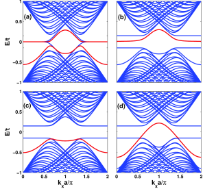
In Fig. 2, we plot the band spectra of the two configurations shown in Fig. 1 with different parameters. Note that here is set zero in all cases of Fig. 2. First, to easily capture the changes in the band structure induced by a staggered potential, the band spectrum with a line defect is firstly plotted with parameter in Fig. 2(a). It can be found that two additional states (red lines) are included in contrast to the band structure of pristine graphene. Cresti Note that due to the two additional states the particle-hole symmetry is broken, which probably gives rise to some intriguing properties in this system. Gunlycke ; Bahamon ; Okada ; Kou In Fig. 2(b-d), a bulk band gap can be observed for two configurations when choosing a nonzero staggered potential. Importantly, when for the configuration 1, an extra state due to the line defect can be seen in the gap and fills approximately half of the band gap. However, this special state in the band gap due to the line defect disappears completely when we turn to the band spectrum of the configuration 2 with as shown in Fig. 2(c). Furthermore, this state appears again and becomes gapless when is tuned to the value of for the configuration 2 in Fig. 2(d)
III.2 The properties of the gapless state
Some questions from these new results naturally arise such as: What characteristics does the special state due to the line defect shown in Fig. 2(d) have, and are there some novel applications in graphene electronics related to these different band spectra? These are the questions of interest in this paper. For simplicity, we will focus mainly on the band spectrum in Fig. 2(d) with because the gapless state has, in general, much more fascinating physics and all band spectra should have the same origin. In fact, the following discussions can also apply to other cases equally.
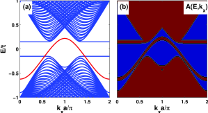
Sometimes, the band spectrum for an infinitely long ribbon is dependent on ribbon’s width. For example, graphene ribbon with armchair edges exhibits the characteristics of a metal or an insulator depending on the ribbons’ width. This motivates us to study the dependence of the band spectrum on the width of ribbon. In contrast to the width of ribbon with in Fig. 2(d), the gapless state still exists and no noticeable changes can be observed in the whole band spectrum when setting in Fig. 3(a). In fact, regardless of what the width of the ribbon is set, the band spectrum looks similar to that in Fig. 3(a).
Furthermore, to provide a further evidence that the gapless state does not disappear and the system at this case always keeps metallic, Fig. 3(b) shows the local density of states (LDOS) nearby the line-defect carbon atoms for an infinitely wide graphene with a line defect (namely, ). Note that LDOS nearby the line defect can be detected experimentally by a scanning tunneling microscope (STM) while in this paper LDOS is obtained theoretically through calculating the Green’s function of the line defect. Jiang In Fig. 3(b), we simply represent LDOS using two different colors, namely the dark red color means a nonzero density of states while the blue color represents a zero value. As shown in Fig. 3(b), besides the disappearance of edge states, LDOS nearby the line defect exhibits nearly the same characteristics as the band spectrum in Fig. 2(d) or Fig. 3(a). The results of LDOS also illustrates that the transport properties of this system are independent of the width of ribbon and should be only related to the line defect.
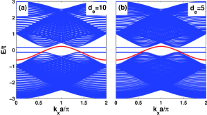
All the above calculations are made on the geometry that the line defect lies in the middle of graphene ribbon. Whether the defect-to-edge distance would affect the band spectrum is worth discussing. Motivated by this idea, we next describe a study of the influence of different defect-to-edge distances on the band spectrum and results are shown in Fig. 4. Here, the distance from the line defect to the top edge of the ribbon is represented as , such as in Fig. 3(a), which means the line defect is exactly in the middle of the ribbon. When shifting the line defect toward the top edge of ribbon with , no obvious changes could be seen in the band spectrum in Fig. 4(a). A similar band spectrum shown in Fig. 4(b) is also observed when the line defect is moved much closer to the top edge of ribbon with . Further calculations with other different show that the band spectrum keeps no noticeable changes if the line defect is not very close to the edge of the ribbon. Therefore, where the line defect lies in the ribbon has almost no influence on the band spectrum, especially the gapless state. Meanwhile, this conclusion can be also applicable to all cases in Fig. 2.
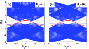
From the discussions above, it is clear that band spectra in Fig. 2 are independent of ribbon’s width and the location of the line defect. To further verify that the gapless state in Fig. 2(d) is not an edge state and not affected by the edge, we consider an additional onsite energy on both edges of the ribbon. Note that the additional onsite energy can be induced due to the surrounding environment or other factors, such as chemical passivation and roughness at the edges. Cresti Here we use the parameter to denote the width of the top (down) edge where the additional onsite energy is induced. In these calculations we set the width of ribbon and a symmetrical configuration is considered.
Fig. 5 shows expanded views of the band spectrum centered on the energy . As expected, no obvious changes in the band spectrum, especially the gapless state, can be seen in Fig. 5(a) with or in Fig. 5(b) with . Thus, the gapless state in Fig. 2(d) should not be an edge state. Besides, it can be concluded from the results in Fig. 5 that the gapless state keeps robust against the variation of edges.
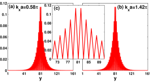
As is known, an effective method to investigate the gapless state in Fig. 2(d) is to examine the distribution of wave functions in real space. In Fig. 6, we investigate the distribution of wave functions for two different momentums. Here, the energy is set , which corresponds an energy level inside band gap and intersects with gapless state at two momentums of and . The horizontal axis in Fig. 6 denotes carbon atom sequence across the ribbon width along the direction. Note that the top lattice site of the ribbon corresponds to , the bottom lattice site is presented by , and additionally the lattice site of the line defect is located at .
In Fig. 6(a), when is chosen to , it can be observed that the wave function mainly localizes around the center of ribbon where the line defect is located. Furthermore, the completely same distribution of the wave functions can be found for the case with the momentum in Fig. 6(b). To seen the wave function’s distribution more clearly, Fig. 6(c) shows a magnification of that in 6(a). Most important is that in Fig. 6(c) the wave function is zero at the 81th site, which exactly corresponds to the site of the line defect. That is to say, the neighbor sites to the line defect mainly contribute to the gapless state inside gap. It is shown by further numerical calculations that the wave function is located mainly around the center of ribbon when the energy is near to the top of valence band (namely, ). However, a complex picture is obtained for the energy far from the top of the valence band.
Based on discussions above, the gapless state in Fig. 2(d) is stable and robust when changing the width of ribbon, the onsite energy of ribbon’s edges, and the position of line defect within the ribbon. Note1 Consequently, using the line defect in graphene shown in Fig. 1, it may be possible to construct a one-dimensional quantum channel to connect various quantum devices. The technology for fabricating and controlling graphene based electronic device is becoming excellent with the boom of graphene research. Neto0 In experiment, it would be feasible to produce a quantum channel in graphene by using a line defect method. Thus, line defects can have a significant contribution in the application of graphene based electrical systems.
III.3 The variation of the band spectra with changing the onsite energy of line defect,
A fundamental question arises if a quantum channel is to be realized using the line defect. That is, is there an easy way to turn on and off the quantum channel through some simple methods, e.g. optical, electronic, and other ways? Motivated by this idea, we study the behavior of the band spectrum when the onsite energy of the line defect in graphene is tuned. In this example, the onsite energy of the line defect could be tuned continuously by a gate voltage embedded below the line defect. Here, other parameters are set and . First, when the onsite energy of line defect is set to be a very large negative value, e.g. , the graphene ribbon can be simply regarded as two separated ribbons divided by the line defect. As seen in Fig. 7(a), the band spectrum has similar characteristics as that of an infinitely long graphene ribbon without a line defect. When changing the onsite energy to the value of , there is no big change in the band spectrum. However, we can see that a state begins to shift upward from the valence band when carefully examining the top of valence band in Fig. 7(b).
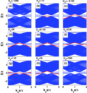
When tuning the onsite energy of the line defect to as shown in Fig. 7(c), a clear gapless state can be observed inside the band gap. Changing from to as shown in Figs. 7(c-e), the gapless state always exists and no obvious change can be observed in the band spectrum. It is interesting to note that the band gap due to staggered potential is precisely . By further increasing , the state inside the gap is shifted upward, but still remains gapless as in Fig. 7(f).
However, the band gap is half-filled by the state of line defect once the onsite energy of line defect rises to the value of in Fig. 7(g). In addition, we observe that a new state starts to emerge from the valence band in Fig. 7(g). Finally, this new state of the line defect takes the place of the state before and the bulk gap is occupied by a gapless state again in Fig. 7(h). With a further growth of onsite energy , this new state is shifted upward and merges into the conduction band when the value of is large enough (approximately at ). The band spectrum with a very large value of is shown in Fig 7(i) and appears very similar to Fig. 7(a), which exhibits a similar band spectrum as that of a graphene ribbon without a line defect. Note that, here the cases of are studied to present what will happen for a very big value of in theory and the similar cases are also studied theoretically in Reference 48. In fact, we just need a small range of , no more than , to tune the state of the line defect from the band gap to the bulk.
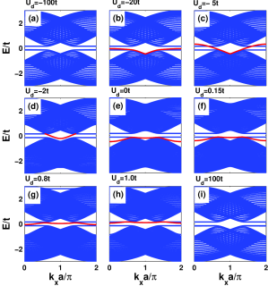
Furthermore, when the sublattice potential is changed from (Fig. 7) to (Fig. 8), similar behaviors of band spectra can be found in Fig. 8. Note that, a excellent gapless state can be observed at , Fig. 8(c); two states of line defect are shifted from the valence band to the conduction band when increasing the onsite energy of line defect gradually. For simplicity, behaviors of band spectra for the configuration 1 are not shown here. Note that, for the configuration 1 with parameters and , only one state of line defect is shifted from the valence band to the conduction band and it never become gapless when increasing the onsite energy of line defect. To sum up, the state inside the gap could be tuned by the onsite energy of the line defect, which can be realized by a gate voltage embedded below the line defect.
III.4 The conductance at various cases
By the Landauer-Büttiker formula, the linear conductance of a mesoscopic system at zero temperature and low bias voltage can be represented as: Song ; Pareek ; SDatta
| (2) |
where is the transmission coefficient from the left lead (source) to the right lead (drain), is the retarded/advanced Green’s function and with the retarded/advanced self-energy . For simplicity, The size of the central region is denoted by integers M and N, which represent the width and length, respectively. For example, in Fig. 1, the width with , and the length with .
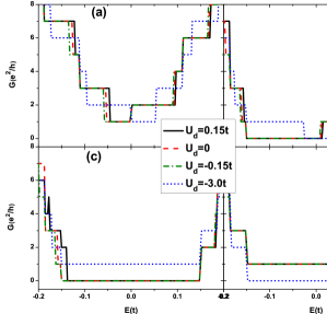
In Fig. 9, we plot the conductance for two configurations with different staggered potentials and onsite energies for the line defect. There are four main conclusions that can be made from the results shown in Fig. 9. (1) For the configuration 1 or 2 with in Fig. 9(a), an asymmetrical conductance plateau is observed near the Dirac point, which indicates that the particle-hole symmetry is broken due to the existence of line defect. Because there is no band gap at this case, the conductance would change but always keeps no less than for the different onsite energies of the line defect, . (2) For the configuration 1 with , the conductance in Fig. 9(b) jumps from zero to a quantum plateau for while for it falls from a quantum plateau to zero when increasing the Fermi energy from to . (3) In all plots shown in Fig. 9, the conductance curves keep almost unchanged for . However, for , the conductance always shows great differences from that at the other cases with . This is because, in this case, the line-defect state is greatly affected by such large onsite energy of the line defect and thus far away from the original position. (4) Specially, it is observed in Figs. (c) and (d) that the conductance exhibits either a quantum plateau or zero for the energy inside the band gap. For example, in Fig. 4(d), the quantum plateau has almost no variation when . However, the conductance falls to zero for a large onsite energy of the line defect, , because here the line-defect state is far from the gap and completely merges into the bulk band.
Note that all of the observations about the conductance in Fig. 9 are consistent with the characteristics of the band spectra discussed above in Fig. 7 and Fig. 8. In summary, the graphene with a line defect can exhibit an insulator or a metal with a quantum conductance . Therefore, a quantum channel can be constructed using the line defect and importantly it can be turned on or off easily by changing the onsite energy of the line defect.
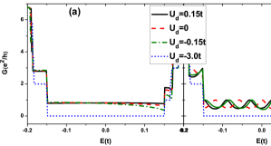
In general, vacancies or point defects can affect the transport of a line defect greatly. Bahamon Thus, we consider the influence of vacancy on the transport properties of a line defect and the results are shown in Fig. 10. Here, we assume that a vacancy is generated due to two-atom missing from the line defect, which lie at the sites in the same supercell (such as the two red sites in the red rectangle in Fig.1). Meanwhile, in order to minimize the total energy, the carbon atom’s electrons, which lie at the up and down carbon atoms sites nearby the missing atoms, can now hop directly with strength . As shown in Fig. 10(a), although the conductance has a dip to zero for Fermi energies near the bottom of the conductance band, the quantum conductance plateau is robust for Fermi energies near the top of the valence band. This conclusion is general for all curves when . Additionally, when considering two vacancies in a line defect, a completely different picture is presented in Fig. 10(b). Here, the size of the central region is chosen to be and , and two vacancies of the line defect lie at both ends of the line defect in the central region, (the distance of two vacancies is therefore denoted by with ). As shown in Fig. 10(b), the quantum conductance plateau disappears and is replaced by the conductance oscillations. That is because a standing wave is formed due to reflections by the two vacancies. Therefore, the oscillations shown in this energy range are simply the Fabry-Perot interference effect due to the broken translational symmetry introduced by the vacancies in the line defect. Bahamon
IV CONCLUSIONS
With considering a broken bulk inversion symmetry due to a staggered potential, we study the graphene with a line defect and find that distinctive band spectra could be obtained for different configurations which can be attributed to different distributions of a staggered potential. In particular, a gapless state exists for a given configuration which holds a mirror symmetry with respect to the line defect. Further calculations show that this special band structure is independent of the width of ribbon, the onsite energy of ribbon’s edges, and the location of line defect within the ribbon. Through analyzing the distribution of wave function of the gapless state, it is found that this gapless state should be attributed to the line defect. In addition, the gapless state is robust against a weak perturbations of the onsite energy of the line defect, e.g., keeps always gapless when [shown in Fig. 9].
These exotic characteristics of line defects illustrate that a quantum channel could be fabricated using the line defect. In particular, the turning on or off of this quantum channel can be realized by a gate voltage embedded below the line defect. The line defect could then be used to connect different quantum devices and serve as a quantum channel to transport quantum signals between devices. All the results in this study support the idea that the line defect is a useful structure for the implementation of a quantum channel in the field of microelectronics.
ACKNOWLEDGMENTS
We are grateful to Tao Qin and Yanyang Zhang for their helpful discussions. Juntao Song is supported by NSFC under Grant No. 11047131, No. 11147172, RFDPHE-China under Grant No. 20101303120005, and SFHP under Grant No.A2012205069. Hua Jiang is supported by China Post-doctroal Science Foundation under Grant No. 20100480147 and No. 201104030. Qing-feng Sun and X.C. Xie are supported by NSFC under Grant No. 11074174, No. 10974236, and China-973 program.
References
- (1) K. S. Novoselov, A. K. Geim, S. V. Morozov, D. Jiang, Y. Zhang, S. V. Dubonos, I. V. Grigorieva, and A. A. Firsov, Science 306, 666 (2004).
- (2) K. S. Novoselov, A. K. Geim, S. V. Morozov, D. Jiang, M. I. Katsnelson, I. V. Grigorieva, S. V. Dubonos, and A. A. Firsov, Nature (London) 438, 197 (2005).
- (3) A. K. Geim and K. S. Novoselov, Nat. Mater., 6, 183 (2007).
- (4) A. K. Geim and A. H. MacDonald, Phys. Tod. 60, 35 (2007); K. S. Novoselov, et al., PNAS 102, 10451 (2005).
- (5) P. Avouris, Z. Chen, and V. Perebeinos, Nat. Nanotech. 2, 605 (2007); P. R. Wallace, Phys. Rev. 71, 622 (1947);G. W. Semenoff, Phys. Rev. Lett. 53, 2449 (1984).
- (6) A. H. C. Neto, F. Guinea, N. M. R. Peres, K. S. Novoselov, and A. K. Geim, Rev. Mod. Phys. 81, 109 (2009).
- (7) K. I. Bolotin, K. J. Sikes, Z. Jiang, G. Fudenberg, J. Hone, P. Kim, and H. L. Stormer, Solid State Commun. 146, 351 (2008).
- (8) A. A. Balandin, S. Ghosh, W. Bao, I. Calizo, D. Teweldebrhan, F. Miao, and C. N. Lau, Nano Lett. 8, 902 (2008).
- (9) D. S. L. Abergel, V. Apalkov, J. Berashevich, K. Ziegler, and T. Chakraborty, Adv. Phys. 59, 261 (2010).
- (10) F. Schwierz, Nat. Nanotech. 5, 487 (2010).
- (11) N. M. R. Peres, Rev. Mod. Phys. 82, 2673 (2010).
- (12) M. T. Lusk and L. D. Carr, Phys. Rev. Lett. 100, 175503 (2008).
- (13) M. T. Lusk and L. D. Carr, Carbon 47, 2226 (2009).
- (14) L. D. Carr and M. T. Lusk, Nat. Nanotech. 5, 316 (2010).
- (15) F. Banhart, J. Kotakoski, and A. V. Krasheninnikov, ACS Nano 5, 26 (2011).
- (16) P. Esquinazi, D. Spemann, R. Hhne, A. Setzer, K.-H. Han, and T. Butz, Phys. Rev. Lett. 91, 227201 (2003).
- (17) P. O. Lehtinen, A. S. Foster, Yuchen Ma, A. V. Krasheninnikov, and R. M. Nieminen, Phys. Rev. Lett. 93, 187202 (2004).
- (18) M. A. H. Vozmediano, M. P. Lpez-Sancho, T. Stauber, and F. Guinea, Phys. Rev. B 72, 155121 (2005).
- (19) S. Okada, K. Nakada, K. Kuwabara, K. Daigoku, and T. Kawai, Phys. Rev. B 74, 121412(R) (2006).
- (20) O. V. Yazyev and L. Helm, Phys. Rev. B 75, 125408 (2007).
- (21) Y. Wang, Y. Huang, Y. Song, X. Zhang, Y. Ma, J. Liang, and Y. Chen, Nano Lett. 9, 220 (2009).
- (22) J. C̆ervenka, M. I. Katsnelson and C. F. J. Flipse, Nat. Phys. 5, 840 (2009).
- (23) M. M. Ugeda, I. Brihuega, F. Guinea, and J. M. Gómez-Rodríguez, Phys. Rev. Lett. 104, 096804 (2010).
- (24) Y. C. Chang and S. Haas, Phys. Rev. B 83, 085406 (2011).
- (25) J. Chen, L. Li, W. G. Cullen, E. D. Williams, and M. S. Fuhrer, Nat. Phys. 7, 535 (2011).
- (26) J. C̆ervenka and C. F. J. Flipse, Phys. Rev. B 79, 195429 (2009).
- (27) N. M. R. Peres, F. Guinea, and A. H. Castro Neto, Phys. Rev. B 73, 125411 (2006).
- (28) O. V. Yazyev, and S. G. Louie, Nat. Mater. 6, 806 (2010).
- (29) A. Mesaros, S. Papanikolaou, C. F. J. Flipse, D. Sadri and J. Zaanen, Phys. Rev. B 82, 205119 (2010).
- (30) S. Malola, H. Hakkinen, and P. Koskinen, Phys. Rev. B 81, 165447 (2010).
- (31) Y. Liu and B. I. Yakobson, Nano Lett. 10, 2178 (2010).
- (32) R. Grantab, V. B. Shenoy, and R. S. Ruoff, Science 330, 946 (2010).
- (33) O. V. Yazyev, and S. G. Louie, Phys. Rev. B 81, 195420 (2010).
- (34) C. Weeks, J. Hu, J. Alicea, M. Franz, and R. Wu, Phys. Rev. X 1, 021001 (2011).
- (35) H. Zhang, C. Lazo, S. Blügel, S. Heinze, and Y. Mokrousov, Phys. Rev. Lett. 108, 056802 (2012).
- (36) K. T. Chan, J. B. Neaton, and M. L. Cohen, Phys. Rev. B 77, 235430 (2008).
- (37) J. Ding, Z. Qiao, Wanxiang Feng, Y. Yao, and Q. Niu, Phys. Rev. B 84, 195444 (2011).
- (38) J. Lahiri, Nat. Nanotech. 5, 326 (2010).
- (39) P. A. Thrower, in Chemistry and Physics of Carbon, edited by P. L. Walker Jr. (Dekker, New York, 1969), Vol. 5, p. 262; A. Stone and D. J. Wales, Chem. Phys. Lett. 28, 501 (1986).
- (40) D. Gunlycke and C. T. White, Phys. Rev. Lett. 106, 136806 (2011).
- (41) D. A. Bahamon, A. L. C. Pereira, and P. A. Schulz, Phys. Rev. B 83, 155436 (2011).
- (42) S. Okada, T. Kawai, and K. Nakada, J. Phys. Soc. Jap. 80, 013709 (2011).
- (43) L. Kou, C. Tang, W. Guo, and C. Chen, ACS Nano 5, 1012 (2011).
- (44) J. N. B. Rodrigues, P. A. D. Gonçalves, N. F. G. Rodrigues, R. M. Ribeiro, J. M. B. Lopes dos Santos, and N. M. R. Peres, Phys. Rev. B 84, 155435 (2011).
- (45) F. D. M. Haldane, Phys. Rev. Lett. 61, 2015 (1988).
- (46) C. L. Kane and E. J. Mele, Phys. Rev. Lett. 95, 226801 2005; 95, 146802 (2005).
- (47) W. Yao, S. A. Yang, and Q. Niu, Phys. Rev. Lett. 102, 096801 (2009);
- (48) Y.-W. Son, M. L. Cohen, and S. G. Louie, Phys. Rev. Lett. 97, 216803 (2006); A. R. Akhmerov and C. W. J. Beenakker, Phys. Rev. B 77, 085423 (2008); A. W. W. Ludwig, M. P. A. Fisher, R. Shankar, and G. Grinstein, Phys. Rev. B 50, 7526 (1994).
- (49) G. Giovannetti, P. A. Khomyakov, G. Brocks, P. J. Kelly, and J. van den Brink, Phys. Rev. B 76, 073103 (2007); X. Zhong, Y. K. Yap, R. Pandey, and S. P. Karna, Phys. Rev. B 83, 193403 (2011); B. Sachs, T. O. Wehling, M. I. Katsnelson, and A. I. Lichtenstein, Phys. Rev. B 84, 195414 (2011).
- (50) C. C. Liu, W. Feng, and Y. Yao, Phys. Rev. Lett. 107, 076802 (2011); C. C. Liu, H. Jiang, and Y. Yao, Phys. Rev. B 84, 195430 (2011).
- (51) A. Cresti, N. Nemec, B. Biel, G. Niebler, F. Triozon, G. Cuniberti, and S. Roche, Nano Res. 1, 361 (2008).
- (52) H. Jiang, Z. Qiao, Haiwen Liu, and Qian Niu, Phys. Rev. B 85, 045445 (2012).
- (53) The line defect state of the configuration 1 is also stable and robust when changing the width of ribbon, the onsite energy of ribbon’s edges, and the position of line defect within the ribbon. Here we main focus the gapless state of configuration 2 and therefore omit the discussion of the configuration 1 for simplicity.
- (54) H. Jiang, L. Wang, Q.-F. Sun, and X. C Xie, Phys. Rev. B 80, 165316 (2009); J. Song, H. Liu, H. Jiang, Q.-F. Sun, and X. C. Xie, Phys. Rev. B 85, 195125(2012).
- (55) T. P. Pareek, Phys. Rev. Lett. 92, 076601 (2004); Y. Xing, Q.-F. Sun, and J. Wang, Phys. Rev. B 73, 205339 (2006);Phys. Rev. B 80, 235411 (2009); Juntao Song, Q.-F. Sun, Jinhua Gao, and X. C. Xie, Phys. Rev. B 75, 195320 (2007).
- (56) Electronic Transport in Mesoscopic Systems, edited by S. Datta (Cambridge University Press 1995).