Nanoelectromechanics of shuttle devices
Abstract
A single-electron tunneling (SET) device with a nanoscale central island that can move with respect to the bulk source- and drain electrodes allows for a nanoelectromechanical (NEM) coupling between the electrical current through the device and mechanical vibrations of the island. Although an electromechanical "shuttle" instability and the associated phenomenon of single-electron shuttling were predicted more than 15 years ago, both theoretical and experimental studies of NEM-SET structures are still carried out. New functionalities based on quantum coherence, Coulomb correlations and coherent electron-spin dynamics are of particular current interest. In this article we present a short review of recent activities in this area.
pacs:
73.23.-b, 72.10.Fk, 73.23.Hk, 85.85.+jI Introduction
Electro-mechanical and mechano-electrical transductions phenomena have historically contributed greatly to the advancement of technology in our society. Today, such operations can be achieved on the single-molecular level with obvious advantages brought about by the miniaturization of the devices involved. In addition qualitatively novel functionalities become available due to new physics that becomes relevant in materials structured on the nanometer length scale. Quantum mechanics and electron-electron (Coulomb) correlations are defining ingredients of mesoscopic physics, which applies to nanoscale devices whose properties may be determined by a single or a few degrees of freedom. As a result there is a possibility and also an advantage to be gained by taking quantum coherence into account when designing electro-mechanical devices for the purpose of quantum manipulation and quantum communication.
The single-electron tunneling (SET) transistor is a nanodevice with particularly prominent mesoscopic features. Here, the Coulomb blockade of single-electron tunneling at low voltage bias and temperature coulombblockade makes Ohm’s law for the electrical conductance invalid in the sense that the electrical current is not necessarily proportional to the voltage drop across the device. Instead, the current is due to a temporally discrete set of events where electrons tunnel quantum-mechanically one-by-one from a source to a drain electrode via a nanometer size island (a “quantum dot"). This is why the properties of a single electronic quantum state are crucial for the operation of the entire device.
Since the probability for quantum mechanical tunneling is exponentially sensitive to the tunneling distance it follows that the position of the quantum dot relative to the electrodes is crucial. On the other hand the strong Coulomb forces that accompany the discrete nanoscale charge fluctuations, which are a necessary consequence of a current flow through the SET device, might cause a significant deformation of the device and move the dot, hence giving rise to a strong electro-mechanical coupling. This unique feature makes the so-called nanoelectromechanical SET (NEM-SET) devices, where mechanical deformation can be achieved along with electronic operations, to be one of the best nanoscale realizations of electromechanical transduction.
In this review we will discuss some of the latest achievements in the nano-electromechanics of NEM-SET devices focusing on the new functionality that exploits quantum coherence in both the electronic and the mechanical subsystems. The choice of materials for making a NEM-SET device brings an additional dimension to exploring its quantum performance. By choosing superconductors or magnets as components of the device one may, e.g., take advantage of a macroscopic ordering of electrons with respect to both their charge and spin. We will discuss how the electronic charge as well as the electronic spin contribute to electromechanical and mechano-electrical transduction in a NEM-SET device. New effects appear also due to the high mechanical deformability of molecular NEM-SET structures (polaronic effects) which could be accompanied with effects of strong electron-electron interactions (Coulomb blockade and Luttinger liquid phenomena) as well as effects caused by strong tunneling coupling (Kondo- nano-mechanics).
The phenomenon of shuttling and the sensitivity of electronic tunneling probabilities to mechanical deformation of the device are in the focus of the present review. In this sense it is is an update of our earlier reviews of shuttling shuttlerev1 ; shuttlerev2 ; shuttlerevfnt . Other aspects of nanoelectromechanics are only briefly discussed here. We refer readers to the well-known reviews of Refs. blencowe, ; roukes1, ; roukes2, ; cleland, ; zant, on nanoelectromechanical systems for additional information.
This review is organized as follows. In Section II we introduce the basic concepts of electron shuttling (Subsection II.A) and consider the influence of polaronic effects on the shuttle instability (Subsection II.B). In the end of this subsection the quantum shuttle is introduced and briefly discussed. Section III deals with the shuttling of Cooper pairs (Subsection III.A) and polaronic effects on the Josephson current through a vibrating quantum dot (Subsection III.B). A novel phenomenon — magnetic shuttling — is considered in Section IV, where the effects of spin-controlled shuttling of electric charge (Subsection IV.A), the spintro-mechanics of the magnetic shuttle (Subsection IV.B) and mechanical transportation of magnetization (Subsection IV.C) are discussed. In the end of Section III the Kondo regime of electron shuttling is reviewed (Subsection IV.D). Recent experiments on the observation of electron shuttling are briefly discussed in Section V. Section VI summarizes the latest theoretical achievements in nanoelectromechanics of shuttle devices.
II Shuttling of single electrons
A single-electron shuttle can be considered as the ultimate miniaturization of a classical electric pendulum capable of transferring macroscopic amounts of charge between two metal plates. In both cases the electric force acting on a charged “ball" that is free to move in a potential well between two metal electrodes kept at different electrochemical potentials, , results in self-oscillations of the ball. Two distinct physical phenomena, namely the quantum mechanical tunneling mechanism for charge loading (unloading) of the ball (in this case more properly referred to as a grain) and the Coulomb blockade of tunneling, distinguish the nanoelectromechanical device known as a single-electron shuttle shuttleprl (see also electrinst ) from its classical textbook analog. The regime of Coulomb blockade realized at bias voltages and temperatures (where is the charging energy, is the grain’s electrical capacitance) allows one to consider single electron transport through the grain. Electron tunneling, being extremely sensitive to the position of the grain relative to the bulk electrodes, leads to a shuttle instability — the absence of any equilibrium position of an initially neutral grain in the gap between the electrodes.
In Subsection A below we consider the characteristic features of the single-electron shuttle in the case when the shuttle dynamics can be treated as classical motion. Quantum corrections to this picture are then discussed in Subsection B.
II.1 Shuttle instability in the quantum regime of Coulomb blockade
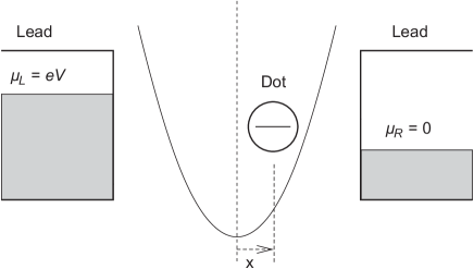
Theoretically, it is convenient to study the single-electron shuttle in an approach shuttlefedor where the grain is modeled as a single-level quantum dot (QD) that is weakly coupled (via a tunnel Hamiltonian) to the electrodes (see Fig. 1). The Hamiltonian corresponding to this model reads
| (1) |
where the Hamiltonian
| (2) |
describes noninteracting electrons in the left () and right () leads, which are kept at different chemical potential ; creates (annihilates) an electron with momentum in lead . The QD Hamiltonian takes the form
| (3) |
where is the creation (destruction) operator for an electron on the dot, is the energy of the resonant level, is the dimensionless coordinate operator (normalized by the amplitude of zero-point fluctuations, , is the mass of QD), is the corresponding momentum operator (), is the frequency of vibrons and is the electromechanical interaction energy. The physical meaning of the second term in Eq. (3) is the interaction energy due to the coupling of the electron charge density on the dot with the electric potential , where is the electric field in the gap between electrodes ( is the distance between the electrodes, is the center-of-mass coordinate of the quantum dot). In this case the coupling "constant" from Eq. (3) is a linear function of bias voltage .
The tunneling Hamiltonian in Eq. (1) differs from its standard form. The explicit coordinate dependence of the tunneling matrix elements introduces additional electron-vibron interactions (additional to those described by the second term of Eq. (3). These result in the appearance of quantum cohesive forces , , where
| (4) |
Here is the bare tunneling amplitude, which corresponds to a weak dot-electrode coupling, is a dimensionless parameter ( is the electron tunneling length) that characterizes the sensitivity of the tunneling matrix elements to a shift of the dot center-of-mass coordinate with respect to its equilibrium () position.
In this Section we are interested in the classical shuttle motion induced by an applied voltage . Here the average is taken with the statistical operator obeying the Liouville-von Neumann equation
| (5) |
For a weak electron-vibron interaction characterized by the dimensionless coupling constant , one can neglect the effects () of zero-point QD fluctuations (see below). In this case the classical dot coordinate is governed by Newton’s equation shuttlefedor
| (6) |
where the average force consists of two terms: the electric force acting on the accumulated charge on the QD, and the cohesive force, , produced by the position-dependent hybridization of the electronic states of the grain and the leads. The evaluation of both forces can be done analytically shuttlefedor ; fedorets , either by solving Heisenberg equations of motion for the fermion operators (, ) or by using the Keldysh Green’s function approach. The nonlinear Eq. (6) for the classical shuttle motion can be analyzed in two cases: (i) near the shuttle instability (), and (ii) for the developed shuttle motion (finite , small ).
For weak electromechanical coupling it was shown shuttlefedor that the amplitude of initially small oscillations starts to grow exponentially () if , which means that the threshold voltage for the shuttle instability is .
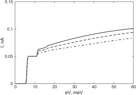
The rate of growth of the instability, , depends on the level width , where ( is the density of states, which is assumed to be an energy independent quantity in the wide band approximation glazshekhter ; wba ) and on the strengths of the electromechanical coupling . It was also shown shuttlefedor that even in the absence of mechanical friction, which can be taken into account phenomenologically by adding to Eq. (6) the dissipative term , the instability develops into a limit cycle. This is in contrast with a classical shuttle shuttleprl , where stability of the system can be achieved, only at finite mechanical dissipation . In the considered model the effective dissipation is provided by the hybridization () of the resonant level with the metallic leads.
Notice that the cohesive force is unimportant for the developed shuttle motion. However, this exchange interaction along with the direct electric coupling () determines the growth rate of the shuttle instability, which demonstrates the important role of electron tunneling in the dynamics of single electron shuttling.
II.2 Strong electron-vibron interaction and polaronic effects in electron shuttling
What is the role of quantum effects in the vibrational subsystem? It is known that the electron-vibron interaction (second term in Eq. (3)) results in vibron-assisted electron tunneling glazshekhter (the appearance of inelastic channels) and for in strong suppression of the probability of electron transfer through the elastic channel (Franck-Condon blockade 116 , see also the reviews ratner, ; palevski, ). Could these vibrational effects influence the single-electron shuttling phenomenon?
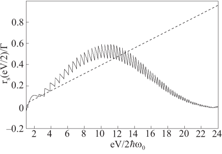
The problem just stated was considered in Ref. gleb, . Quantum fluctuations of the dot coordinate can be taken into account by replacing the operator in Eqs. (3,4) by , where . The “quantum" part of the electron-vibron interaction () in Eq. (3) can be eliminated in the Hamiltonian (4) by a standard trick - the Lang-Firsov unitary transformation mahan ; langfirsov , where . After the unitary transformation the electron-vibron coupling appears in the tunneling Hamiltonian in the form of an additional operator factor . Since in the transformed Hamiltonian electron-vibron interactions enter only in the tunneling Hamiltonian, the problem can be solved in perturbation theory with respect to the bare tunneling width . In the lowest order of perturbation theory the averages of bosonic and fermionic operators are decoupled and the bosonic correlation functions can be evaluated analytically ( denotes an average with respect to the noninteracting Hamiltonian ). The result gleb is an increment rate of the shuttle instability that is valid both for weak and strong electromechanical coupling. For a symmetric junction and it reads
| (7) |
where
| (8) |
and the symbol here denotes the integer part. In the limit of weak electromechanical couplings , Eq. (7) reproduces the result of Ref. shuttlefedor, , , which predicts a linear dependence of on the bias voltage, . Two new factors in Eq. (7) (the exponential factor and the sum over open inelastic channels) reflect the influence of two major vibrational effects - the Franck-Condon blockade and vibron-assisted electron tunneling - on the shuttle instability. Since the dimensionless coupling is always small for molecular devices, the main quantum effect of vibrations is the “polaronic" narrowing of the bare tunneling width . It increases with the increase of the number of new channels () and reaches its maximum at ( is the distance between electrodes, is the mass of the vibrating molecule). A nonmonotonic dependence of the increment rate of the shuttle instability on is shown in Fig. 3. One can see that an instability takes place in a finite interval of bias voltages due to the Franck-Condon blockade. Besides, at low temperatures, , the increment rate oscillates with a period of order and with a relatively large amplitude. Notice that at low voltages and hence “polaronic" effects could not affect the “intrinsic" shuttle instability, which takes place at . However, if the grain is pinned or if there is strong friction in the system, , the shuttle instability takes place at much higher voltages when . In this case large oscillations of the increment parameter could lead to unusual behavior of the I-V characteristics for a shuttle-based single-electron transistor. A small change in bias voltage (smaller than ) would take the system from the shuttle regime of transport (with strongly enhanced electron tunneling probability) to the ordinary regime of tunnel transport (small tunneling probability) and the other way around. Therefore one can expect pronounced negative differential conductance (NDC) features (on the scale of ) in the current voltage characteristics (see also Refs. 111, ; 116, ).
It is interesting to note that in the absence of mechanical damping, (), the threshold voltage for single electron shuttling is determined by the vibron energy shuttlefedor This quantum threshold value indicates where the process of inelastic electron tunneling (with emission of a vibron) becomes energetically available. In the realistic case of finite friction the threshold bias voltage is found by solving the equation , where is defined in Eq. (7) (see Fig. 3). In the limit of weak electromechanical coupling one gets for the threshold electric field () the result
| (9) |
which has a linear dependence on the rate of dissipation . The exponential increase (above threshold) of the amplitude of the shuttle motion means that for the fully developed (stationary) shuttle motion . However, at the initial stage of the instability the oscillation amplitude can be of the order of and the classical treatment of shuttle motion ceases to be valid.
A fully quantum-mechanical approach to single electron shuttling was developed in Refs. fundam, ; novotny, ; quanshuttle, , where it was shown that the shuttle instability (exponential increase of and ) in the limit occurs for a threshold electric field that coincides with Eq. (9), found in a quasiclassical approach. By using the Wigner distribution function, which allows one to visualize the behavior of a quantum system in phase space novotny , two different regimes of single electron shuttling were found. The classical regime (small fluctuations around the stationary trajectory ) is realized for the fields , where quanshuttle
| (10) |
(), i.e. in the case of weak mechanical dissipation and for large bias voltages. For low biases, when the electric fields, acting on the charged QD are in the interval , the shuttle regime has a specific quantum character. The Wigner function is strongly smeared around the classical trajectory. It is concentrated in a region between two circles with radii and for . This behavior is characterized by pronounced quantum fluctuations and can be interpreted as a quantum shuttle. It is difficult to detect a quantum shuttle by measuring the average current since its qualitative behavior has no distinctive features in comparison with the classical shuttle. The noise properties (and in general the full counting statistics) of NEMS will be crucial for detecting single-electron shuttling.
III Mechanically mediated superconductivity and polaronic effects in the Josephson current
Shuttling of electric charges between nonsuperconducting electrodes by itself does not require phase coherence. Even in the quantum regime of the Coulomb blockade, when only a single (resonant) level is involved in electron transport, phase coherent effects have little influence on electron shuttling. This is not the case for magnetic and superconducting leads. Magnetic exchange forces make the coherent electron-spin dynamics important for electron shuttling. Superconducting transport is by definition a phase coherent phenomenon and thus Cooper-pair shuttling has to be strongly different from single-electron shuttling.
In this Section we consider shuttling of Cooper pairs between two superconducting electrodes (subsection A) and the influence of vibrational modes on the Josephson current.
III.1 Shuttling of Cooper pairs
The main requirement for the observation of a mechanically mediated Josephson current 2.5 ; 2.6 is that phase coherence is preserved during the transportation of Cooper pairs between the two superconducting leads, and during the process of transferring charge between the bulk superconductors and a movable superconducting grain. This requirement can be fulfilled if the superconducting grain is small enough to be in the Coulomb blockade regime coulombblockade (see also vanhouten ) so that it can play the role of a single-Cooper-pair box 2.2 (see also naka ; devo ). The implication is that the characteristic energy scales of the small superconducting grain – the Josephson energy (where is the critical current) and the charging energy (where is the grain capacity) – have to obey the double inequality (where is the superconducting gap) while the temperature has to be low enough to make . In this regime the single-electron states on the grain are energetically unfavorable (the parity effect quant ; 2.2 ) and the superconducting properties of the system can be described by a two-level model (see for example the review 2.1 ). The corresponding state vector of a single-Cooper-pair box is a coherent superposition of the states with and Cooper pairs ( more generally states with the different number of Cooper pairs: and ) on the grain. For a movable Cooper pair box the energy scale for mechanical vibrations has to be much smaller then all other energy scales. This additional requirement prevents the creation of quasiparticles and allows one to consider the mechanical motion of the grain as an adiabatic process.
The Hamiltonian of the system is expressed in terms of the Cooper pair number operator for the grain and the phases of the superconducting leads, :
| (11) |
The operator changes the number of Cooper pairs on the grain. An essential specific feature here is the dependence of the charging energy difference and the coupling energies ( is the distance between the grain and the respective lead) on the instantaneous position of the superconducting grain.
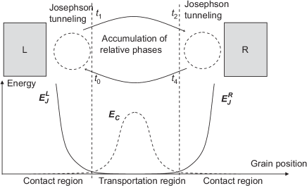
It is useful to separate the adiabatic motion of the single-Cooper-pair box between the two superconducting electrodes into two different parts: (i) the free motion ( transportation region in Fig. 4), and (ii) the process of loading and unloading of charge near the leads ( contact region in Fig. 4). During the free motion, when the Josephson energy is negligibly small and the Coulomb term dominates, the dynamics of the qubit is reduced to the time evolution of the relative phase due to the second term in Eq. (11), . In general the accumulated phases are different for left-to-right () and right-to-left () motion; . The coherent exchange of a Cooper pair between the grain and the lead [stage (ii)] is characterized by the dimensionless Josephson coupling strength , where is the time spent by the grain in contact with the lead (see Fig. 4). The superconducting phase difference , the dynamical phases and the Josephson coupling strength fully control the behavior of the Josephson current. The characteristic value of the mechanically assisted supercurrent (the “critical" current ) for a periodic motion of the grain (with frequency ) and for strong Josephson coupling is determined by the mechanical frequency only, . An analytical expression for the mechanically mediated dc Josephson current was derived in Ref. 2.5, and takes the form
| (12) |
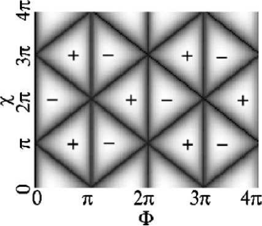
where , . The current Eq. (12) is an oscillating function of the superconducting phase difference (see Fig. 5), which is a spectacular manifestation of a Josephson coupling between the remote superconductors. In the limit of weak coupling and vanishingly small dynamical phase () Eq. (12) is reduced to the standard Josephson formula , where . We see from Eq. (12) that the main qualitative effect of the dynamical phase, which can be controlled by the gate voltage, is a change of the direction of supercurrent (if ). For a given strength of the Josephson coupling the direction of a mechanically mediated supercurrent is determined by the interplay of superconducting () and dynamical () phases. Notice that in Ref. 2.6, it was shown that mechanical transportation of Cooper pairs could establish relative phase coherence between two mesoscopic superconductors if initially they are in states with strong uncorrelated phase fluctuations.
III.2 Josephson current through a vibrating quantum dot
In Section 2 we considered the influence of polaronic effects on the electron shuttle instability. Here we analyze how vibrational degrees of freedom affect the dc Josephson current. When studying the transport properties of a superconductor/quantum dot/superconductor (SQDS) junction we will use the same simple model for the QD as in the previous Section, i.e. we consider a dot with a single energy level that vibrates with angular frequency and is weakly coupled to the superconducting leads. The latter are described by the standard BCS Hamiltonian with order parameter ( is the superconducting gap and is the phase of the order parameter for the left, , and right, , superconductor). The coupling of the dot to the leads is described by a tunnel Hamiltonian, which introduces two energy scales to the problem, viz. the partial level widths . These are very significant for the transport properties.
The QD Hamiltonian reads
| (13) |
where is the destruction (creation) operator for an electron with spin projection , , , is the vibron destruction (creation) operator, is the electron-vibron interaction energy and is the electron-electron interaction energy. In what follows we will assume that is the largest energy scale in the problem. This allows one to neglect quasiparticles (continuum spectrum) when calculating the dc Josephson current.
In general, a coupling to vibrational modes tends to suppress the supercurrent flensberg ; shumeikospec . The suppression mechanism is different for “hard", , and “soft", , vibrons. For hard vibrons and for only the ground state of the vibrational subsystem is involved in Cooper pair transport through a S/QD/S junction. Zero-point fluctuations of the QD result in strong (exponential) renormalization of the electron tunneling probability (“polaronic" narrowing of the level width). For strong electron-vibron coupling — i.e. for , the critical current is exponentially suppressed flensberg , which is a manifestation of the Franck-Condon blockade ratner ; 116 of the supercurrent. Notice, that the Franck-Condon blockade will be partially removed when due to contributions of virtual side-band channels.
The effect of the Franck-Condon blockade was first predicted flensberg for a nonresonant Josephson current , (where is the critical current in the absence of electron-vibron interaction, ). Later, in Ref. zazunovphonon, , it was demonstrated that in the case and an analogous result,
| (14) | |||
holds also for the resonant () current. Notice the extra factor of 2 in the exponent for the nonresonant critical current.
The renormalization of the bare level width is hard to detect in an experiment (since one would have to vary the strength of the electron-vibron interaction). What experimental manifestation of the Franck-Condon blockade can one then look for? For normal transport the answer is that with an increase of temperature the lifting of the blockade is accompanied by a nonmonotonic temperature behavior of the conductance krivetemp ; krivenature . An analogous behavior has been predicted parafilo for superconducting transport, where it is the critical current that reveals an anomalous -dependence. The characteristic temperature which determines the peak in a plot of vs. is determined by the polaronic energy shift . For the critical current increases with temperature (in the regime of temperature-enhanced Josephson coupling) while for the current scales as due to a partial cancelation of Andreev levels contributions. For moderately strong electron-vibron interactions, the crossover from low- regime to -scaling looks like a “resonant" enhancement of the critical current at (see Fig. 6).
For soft vibrons, , the slowly vibrating QD is always able to change its equilibrium position () in order to minimize the total energy. If one neglects electron-electron interactions () the total energy of the weak link can be readily evaluated in the quasiclassical approximation if the dimensionless operator in Eq. (13) is replaced by the classical variable . Then the total energy consists of two terms: (i) the elastic energy, and (ii) the energy of the filled Andreev level
| (15) |
(for simplicity we consider here a symmetric junction). It is easy to see that for coupling strengths such that , a condition which is always fulfilled in the considered limit , the energy minimum corresponds to a shifted QD position, . In an effectively asymmetric junction the resonant () current is suppressed parafilo so that
| (16) |
Unlike the exponential (in the electron-vibron interaction strength) suppression of the critical current induced by zero-point fluctuations of the QD coordinate (), soft vibrons give rise to a power-like (polaronic) suppression of the form . At finite temperatures thermally excited vibron polarons (excitations in the state ) tend to shift the QD towards its spatially symmetric position. This means that , which implies that at low temperatures the current grows with an increase of temperature. The crossover from the regime of a temperature enhanced supercurrent to a standard scaling of the critical current occurs abruptly at parafilo . Therefore, both the Franck-Condon blockade of the supercurrent and the polaronic effects on the Josephson current are manifested in an anomalous (nonmonotonic) temperature behavior of the critical current (see Fig. 6). Estimations show parafilo that for already existing transport experiments on suspended single wall carbon nanotubes (see e.g. sapmaz ) the polaronic temperature is in the range K, which makes the observation of polaronic effects in carbon nanotube-based SNS junctions a feasible experiment.

Finally, we discuss the influence of a charging energy on the polaronic effects on the Josephson current. To this end we first note that the electron-vibron interaction renormalizes the electron-electron correlation energy so that and hence diminishes the strength of the interaction flensberg . It is physically obvious that as long as the effects of a finite charging energy are negligible small. When correlations split the energy level and for the conditions for resonant tunneling of Cooper pairs can not be satisfied. If the electron-electron correlations are so strong that they additionally suppress the critical current by a factor . If the charging energy does changes the value of the low- critical current but it can not influence the predicted anomalous temperature dependence of the current at . What happenes if is an open question, which needs further investigation.
IV Electro - and Spintro - Mechanics of Magnetic shuttle devices
In this Section we will explore new functionalities that emerge when nanomechanical devices are partly or completely made of magnetic materials. The possibility of magnetic ordering brings new degrees of freedom into play in addition to the electronic and mechanical ones considered so far, opening up an exciting perspective towards utilising magneto-electro-mechanical transduction for a large variety of applications. Device dimensions in the nanometer range mean that a number of mesoscopic phenomena in the electronic, magnetic and mechanical subsystems can be used for quantum coherent manipulations. In comparison with the electromechanics of the nanodevices considered above the prominent role of the electronic spin in addition to the electric charge should be taken into account.
The ability to manipulate and control spins via electrical 9 ; 10 ; 11 magnetic 12 and optical 13 means has generated numerous applications in metrology 14 in recent years. A promising alternative method for spin manipulation employs a mechanical resonator coupled to the magnetic dipole moment of the spin(s), a method which could enable scalable quantum information architectures 15 and sensitive nanoscale magnetometry 16 ; 17 ; 18 . Magnetic resonance force microscopy (MRFM) was suggested as a means to improve spin detection to the level of a single spin and thus enable three dimensional imaging of macromolecules with atomic resolution. In this technique a single spin, driven by a resonant microwave magnetic field interacts with a ferromagnetic particle. If the ferromagnetic particle is attached to a cantilever tip, the spin changes the cantilever vibration parameters 21 . The possibility to detect 21 and monitor the coherent dynamics of a single spin mechanically 22 has been demonstrated experimentally. Several theoretical suggestions concerning the possibility to test single-spin dynamics through an electronic transport measurement were made recently 24 ; 25 ; 26 ; 27 . Complementary studies of the mechanics of a resonator coupled to spin degrees of freedom by detecting the spin dynamics and relaxation were suggested in 24 ; 25 ; 26 ; 27 ; 28 ; 29 ; 30 ; 31 and carried out in 32 . Electronic spin-orbit interaction in suspended nanowires was shown to be an efficient tool for detection and cooling of bending-mode nanovibrations as well as for manipulation of spin qubit and mechanical quantum vibrations 33 ; 34 ; 35 .
An obvious modification of the nano-electro-mechanics of magnetic shuttle devices originates from the spin-splitting of electronic energy levels, which results in the known phenomenon of spin-dependent tunneling. Spin-controlled nano-electro-mechanics which originates from spin-controlled transport of electric charge in magnetic NEM systems is represented by number of new magneto-electro-mechanical phenomena.
Qualitatively new opportunities appear when magnetic nanomechanical devices are used. They have to do with the effect of the short-ranged magnetic exchange interaction between the spin of electrons and magnetic parts of the device. In this case the spin of the electron rather than its electrical charge can be the main source of the mechanical force acting on movable parts of the device. This leads to new physics compared with the usual electromechanics of non-magnetic devices, for which we use the term spintro-mechanics. In particular it becomes possible for a movable central island to shuttle magnetization between two magnetic leads even without any charge transport between the leads. The result of such a mechanical transportation of magnetization is a magnetic coupling between nanomagnets with a strength and sign that are mechanically tunable.
In this Section we will review some early results that involve the phenomena mentioned above. These only amount to a first step in the exploration of new opportunities caused by the interrelation between charge, spin and mechanics on a nanometer length scale.
IV.1 Spin-controlled shuttling of electric charge
By manipulating the interaction between the spin of electrons and external magnetic fields and/or the internal interaction in magnetic materials, spin-controlled nanoelectromechanics may be achieved.
A new functional principle — spin-dependent shuttling of electrons — for low magnetic field sensing purposes was proposed by Gorelik et al. in Ref. r88, . This principle may lead to a giant magnetoresistance effect in external magnetic fields as low as 1-10 Oe in a magnetic shuttle device if magnets with highly spin-polarized electrons (half metals r83 ; r84 ; r85 ; r86 ; r87 ) are used as leads in a magnetic shuttle device. The key idea is to use the external magnetic field to manipulate the spin of shuttled electrons rather than the magnetization of the leads. Since the electron spends a relatively long time on the shuttle, where it is decoupled from the magnetic environment, even a weak magnetic can rotate its spin by a significant angle. Such a rotation allows the spin of an electron that has been loaded onto the shuttle from a spin-polarized source electrode to be reoriented in order to allow the electron finally to tunnel from the shuttle to the (differently) spin-polarized drain lead. In this way the shuttle serves as a very sensitive “magnetoresistor" device. The model employed in Ref. r88, assumes that the source and drain are fully polarized in opposite directions. A mechanically movable quantum dot (described by a time-dependent displacement ), where a single energy level is available for electrons, performs driven harmonic oscillations between the leads. The external magnetic field, , is perpendicular to the orientations of the magnetization in both leads and to the direction of the mechanical motion.
The spin-dependent part of the Hamiltonian is specified as
| (17) |
where , are the exchange interactions between the on-grain electron and the left(right) lead, is the gyromagnetic ratio and is the Bohr magneton. The proper Liouville-von Neumann equation for the density matrix is analyzed and an average electrical current is calculated for the case of large bias voltage.
In the limit of weak exchange interaction, one may neglect the influence of the magnetic leads on the on-dot electron spin dynamics. The resulting current is
| (18) |
where is the total tunneling probability during the contact time , while is the rotation angle of the spin during the “free-motion" time.
The theory r88 predicts oscillations in the magnetoresistance of the magnetic shuttle device with a period , which is determined from the equation . The physical meaning of this relation is simple: every time when ( is the spin precession frequency in a magnetic field) the shuttled electron is able to flip fully its spin to remove the “spin-blockade" of tunneling between spin polarized leads having their magnetization in opposite directions. This effect can be used for measuring the mechanical frequency thus providing dc spectroscopy of nanomechanical vibrations.
Spin-dependent shuttling of electrons as discussed above is a property of non-interacting electrons, in the sense that tunneling of different electrons into (and out of) the dot are independent events. The Coulomb blockade phenomenon adds a strong correlation of tunneling events, preventing fluctuations in the occupation of electronic states on the dot. This effect crucially changes the physics of spin-dependent tunneling in a magnetic NEM device. One of the remarkable consequences is the Coulomb promotion of spin-dependent tunneling predicted in Ref. 1, . In this work a strong voltage dependence of the spin-flip relaxation rate on a quantum dot was demonstrated. Such relaxation, being very sensitive to the occupation of spin-up and spin-down states on the dot, can be controlled by the Coulomb blockade phenomenon. It was shown in Ref. 1, that by lifting the Coulomb blockade one stimulates occupation of both spin-up and spin-down states thus suppressing spin-flip relaxation on the dot. In magnetic devices with highly spin-polarized electrons electronic spin-flip can be the only mechanism providing charge transport between oppositely magnetized leads. In this case the onset of Coulomb blockade, by increasing the spin-flip relaxation rate, stimulates charge transport through a magnetic SET device (Coulomb promotion of spin-dependent tunneling). Spin-flip relaxation qualitatively also modifies the noise characteristics of spin-dependent single-electron transport. In Refs. 2, ; 3, it was shown that the low-frequency shot noise in such structures diverges as the spin relaxation rate goes to zero. This effect provides an efficient tool for spectroscopy of extremely slow spin-flip relaxation in quantum dots. Mechanical transportation of a spin-polarized dot in a magnetic shuttle device provides new opportunities for studying spin-flip relaxation in quantum dots. The reason can be traced to a spin-blockade of the mechanically aided shuttle current that occurs in devices with highly polarized and colinearly magnetized leads. As was shown in Ref. 4, the above effect results in giant peaks in the shot-noise spectral function, wherein the peak heights are only limited by the rates of electronic spin flips. This enables a nanomechanical spectroscopy of rare spin-flip events, allowing spin-flip relaxation times as long as s to be detected.
The spin-dependence of electronic tunneling in magnetic NEM devices permits an external magnetic field to be used for manipulating not only electric transport but also the mechanical performance of the device. This was demonstrated in Refs. s90, ; 5, . A theory of the quantum coherent dynamics of mechanical vibrations, electron charge and spin was formulated and the possibility to trigger a shuttle instability by a relatively weak magnetic field was demonstrated. It was shown that the strength of the magnetic field required to control nanomechanical vibrations decreases with an increasing tunnel resistance of the device and can be as low as 10 Oe for giga-ohm tunnel structures.
A new type of nanoelectromechanical self excitation caused entirely by the spin splitting of electronic energy levels in an external magnetic field was predicted in Ref. 6, for a suspended nanowire, where mechanical motion in a magnetic field induces an electromotive coupling between electronic and vibrational degrees of freedom. It was shown that a strong correlation between the occupancy of the spin-split electronic energy levels in the nanowire and the velocity of flexural nanowire vibrations provides energy supply from the source of DC current, flowing through the wire, to the mechanical vibrations thus making possible stable, self-supporting bending vibrations. Estimations made in Ref. 6, show that in a realistic case the vibration amplitude of a suspended carbon nanotube (CNT) of the order of 10 nm can be achieved if magnetic field of 10 T is applied.
IV.2 Spintro-mechanics of magnetic shuttle device
New phenomena, qualitatively different from the electromechanics of nonmagnetic shuttle systems, may appear in magnetic shuttle devices in a situation when short-range magnetic exchange forces become comparable in strength to the long-range electrostatic forces between the charged elements of the device 6 . There is convincing evidence that the exchange field can be several tesla at a distance of a few nanometers from the surface of a ferromagnet radic4 ; radic5 ; radic6 ; radic9 . Because of the exponential decay of the field this means that the force experienced by a single-electron spin in the vicinity of magnetic electrodes can be very large. These spin-dependent exchange forces can lead to various “spintro-mechanical" phenomena.
Mechanical effects produced by a long-range electrostatic force and short-ranged exchange forces on a movable quantum dot are illustrated in Fig. 7.
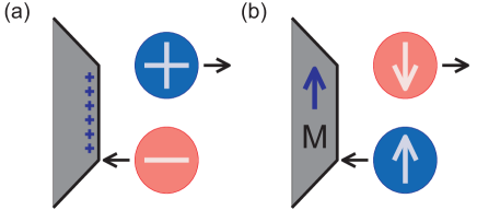
The electrostatic force acting on the dot, placed in the vicinity of a charged electrode (Fig. 7(a)), is determined by the electric charge accumulated on the dot. In contrast, the exchange force induced by a neighboring magnet depends on the net spin accumulated on the dot. While the electrostatic force changes its direction if the electric charge on the dot changes its sign, the spin-dependent exchange force is insensitive to the electric charge but it changes direction if the electronic spin projection changes its sign. A very important difference between the two forces is that the electrostatic force changes only as a result of injection of additional electrons into (out of) the dot while the spintronic force can be changed due to the electron spin dynamics even for a fixed number of electrons on the dot (as is the case if the dot and the leads are insulators). In this case interesting opportunities arise from the possibility of transducing the dynamical variations of electronic spin (induced, e.g., by magnetic or microwave fields) to mechanical displacements in the NEM device. In Ref. 7, a particular spintromechanical effect was discussed – a giant spin-filtering of the electron current (flowing through the device) induced by the formation of what we shall call a “spin-polaronic state".
The Hamiltonian that describes the magnetic nanomechanical SET device in Ref. 7, has the standard form (its spin-dependent part depends now on the mechanical displacement of the dot). Hence , where describes electrons (labeled by wave vector and spin ) in the two leads (). Electron tunneling between the leads and the dot is modeled as
| (19) |
where the matrix elements ( is the characteristic tunneling length) depend on the dot position . The Hamiltonian of the movable single-level dot is
| (20) |
where , is the Coulomb energy associated with double occupancy of the dot and the eigenvalues of the electron number operators is or . The position dependent magnitude of the spin dependent shift of the electronic energy level on the dot is due to the exchange interaction with the magnetic leads. Here we expand to linear order in so that and without loss of generality assume that .
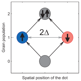
The modification of the exchange force, caused by changing the spin accumulated on the dot, shifts the equilibrium position of the dot with respect to the magnetic leads of the device. Since the electron tunneling matrix element is exponentially sensitive to the position of the dot with respect to the source and drain electrodes one expects a strong spin-dependent renormalization of the tunneling probability, which exponentially discriminates between the contributions to the total electrical current from electrons with different spins. This spatial separation of dots with opposite spins is illustrated in Fig. 8. While changing the population of spin-up and spin-down levels on the dot (by changing e.g. the bias voltage applied to the device) one shifts the spatial position of the dot with respect to the source/drain leads. It is important that the Coulomb blockade phenomenon prevents simultaneous population of both spin states. If the Coulomb blockade is lifted the two spin states become equally populated with a zero net spin on the dot, . This removes the spin-polaronic deformation and the dot is situated at the same place as a non-populated one. In calculations a strong modification of the vibrational states of the dot, which has to do with a shift of its equilibrium position, should be taken into account. This results in a so-called Frank-Condon blockade of electronic tunneling 116 ; ratner . The spintro-mechanical stimulation of a spin-polarized current and the spin-polaronic Franck-Condon blockade of electronic tunneling are in competition and their interplay determines a non-monotonic voltage dependence of the giant spin-filtering effect.
To understand the above effects in more detail consider the analytical results of Ref. 7, . A solution of the problem can be obtained by the standard sequential tunneling approximation and by solving a Liouville equation for the density matrix for both the electronic and vibronic subsystems. The spin-up and spin-down currents can be expressed in terms of transition rates (energy broadening of the level) and the occupation probabilities for the dot electronic states. For simplicity we consider the case of a strongly asymmetric tunneling device. At low bias voltage and low temperature the partial spin current is
| (21) |
where . In the high bias voltage (or temperature) regime, , where the polaronic blockade is lifted (but double occupancy of the dot is still prevented by the Coulomb blockade), the current expression takes the form
| (22) |
where is Bose-Einstein distribution function. The scale of the polaronic spin-filtering of the device is determined by the ratio of the polaronic shift of the equilibrium spatial position of a spin-polarized dot and the electronic tunneling length. For typical values of the exchange interaction and mechanical properties of suspended carbon nanotubes this parameter is about 1-10. As was shown this is enough for the spin filtering of the electrical current through the device to be nearly 100 % efficient. The temperature and voltage dependence of the spin-filtering effect is presented in Fig. 9. The spin filtering effect and the Franck-Condon blockade
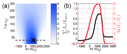
both occur at low voltages and temperatures (on the scale of the polaronic energy; see Fig. 9 (a)). An increase of the voltage applied to the device lifts the Franck-Condon blockade, which results in an exponential increase of both the current and the spin-filtering efficiency of the device. This increase is blocked abruptly at voltages for which the Coulomb blockade is lifted. At this point a double occupation of the dot results in spin cancellation and removal of the spin-polaronic segregation. This leads to an exponential drop of both the total current and the spin polarization of the tunnel current (Fig. 9 (b)). As one can see in Fig. 9 prominent spin filtering can be achieved for realistic device parameters. The temperature of operation of the spin-filtering device is restricted from above by the Coulomb blockade energy. One may, however, consider using functionalized nanotubes pulkin20 or graphene ribbons pulkin21 with one or more nanometer-sized metal or semiconductor nanocrystal attached. This may provide a Coulomb blockade energy up to a few hundred kelvin, making spin filtering a high temperature effect 7 .
IV.3 Mechanically assisted magnetic coupling between nanomagnets
The mechanical force caused by the exchange interaction represents only one effect of the coupling of magnetic and mechanical degrees of freedom in magnetic nanoelectromechanical device. A complementary effect is the of mechanical transportation of magnetization, which we are going to discuss in this subsection.
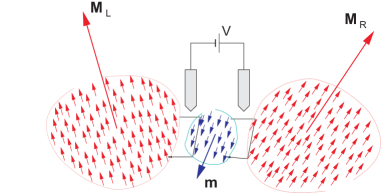
In the magnetic shuttle device presented in Fig. 10, a ferromagnetic dot with total magnetic moment m is able to move between two magnetic leads, which have total magnetization . Such a device was suggested in Ref. 8, in order to consider the magnetic coupling between the leads (which in their turn can be small magnets or nanomagnets) produced by a ferromagnetic shuttle. It is worth to point out that the phenomenon we are going to discuss here has nothing to do with transferring electric charge in the device and it is valid also for a device made of nonconducting material. The main effect, which will be in the focus of our attention, is the exchange interaction between the ferromagnetic shuttle (dot) and the magnetic leads. This interaction decays exponentially when the dot moves away from a lead and hence it is only important when the dot is close to one of the leads. During the periodic back-and-forth motion of the dot this happens during short time intervals near the turning points of the mechanical motion. An exchange interaction between the magnetizations of the dot and a lead results in a rotation of these two magnetization vectors in such a way that the vector sum is conserved. This is why the result of this rotation can be viewed as a transfer of some magnetization from one ferromagnet to the other. As a result the magnetization of the dot experiences some rotation around a certain axis. The total angle of the rotation accumulated during the time when the dot is magnetically coupled to the lead is an essential parameter which depends on the mechanical and magnetic characteristics of the device. The continuation of the mechanical motion breaks the magnetic coupling of the dot with the first lead but later, as the dot approaches the other magnetic lead an exchange coupling is established with this second lead with the result that magnetization which is “loaded" on the dot from the first lead is "transferred" to the this second lead. This is how the transfer of magnetization from one magnetic lead to another is induced mechanically. The transfer creates an effective coupling between the magnetizations of the two leads. Such a non-equilibrium coupling can be efficiently tuned by controlling the mechanics of the shuttle device. It is particularly interesting that the sign of the resulting magnetic interaction is determined by the sign of . Therefore, the mechanically mediated magnetic interaction can be changed from ferromagnetic to anti-ferromagnetic by changing the amplitude and the frequency of mechanical vibrations 8 .
IV.4 Resonance spin-scattering effects. Spin shuttle as a “mobile quantum impurity".
The Kondo effect in electron tunneling results from the spin exchange between electrons in the leads and the island (quantum dot) that couples the leads and manifests itself as a sharp zero bias anomaly in the low-temperature tunneling conductance. Many-particle interactions and the tunneling renormalize the electron spectrum enabling Kondo resonances both for odd gogo and even Pust00 ; Kikoin01 electron occupations. In the latter case the Kondo resonance is caused by the singlet-triplet crossover in the ground state (see glasko for a review). In the simplest case of odd occupancy a cartoon of a quantum well and a schematic Density of States (DoS) is shown in Fig. 11. For simplicity we consider a case when the dot is occupied by one electron (as in a SET transistor). The dot level is not in resonance with the Fermi level of the leads (), but located at an energy , below it. The dot is in the Coulomb blockade regime and the corresponding charging energy is denoted as . The resonance spin scattering results in the formation of a narrow peak in the DoS known as the Abrikosov-Suhl resonance Abrikosov ; Suhl ; Hewson (see Fig. 11, right panel). The width of this resonance defines a unique energy scale, the Kondo temperature , which determines all thermodynamic and transport properties of the SET device through a one-parametric scaling Hewson . The width of the dot level, associated with the tunneling of dot electrons to the continuum of levels in the leads, is assumed to be smaller than the charging energy , providing a condition for an integer valency regime. When the shuttle moves between source (S) and drain (D) (see the lower panel of Fig. 11), both the energy and the width acquire a time dependence. This time dependence results in a coupling between mechanical and electronic degrees of freedom. If a source-drain voltage is small enough () the charge degree of freedom of the shuttle is frozen out while spin plays a very important role in co-tunneling processes. Namely, the dot electron’s spin can be flipped while the electron tunnels from the left to the right lead. Thus, the initial and final states of the quantum impurity can have different spins. This process is accompanied by simultaneous creation of spin excitations in the Fermi sea. The many-electron scattering processes then lead to the formation of an Abrikosov-Suhl resonance. This resonance can be viewed as a Kondo cloud built up from both conduction electrons in the leads and a localized electron in the dot. Since all electrons in the cloud contain information about the same impurity, they are mutually correlated. Thus, NEM providing a coupling between mechanical and electronic degrees of freedom introduces a powerful tool for manipulation and control of the Kondo cloud and gives a very promising and efficient mechanism for electromechanical transduction on the nanometer length scale.
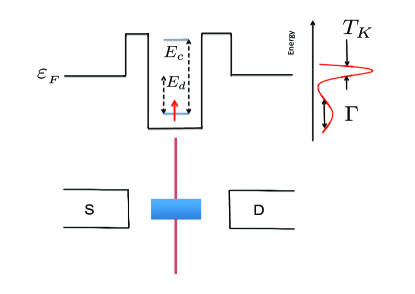
Building on an analogy with the shuttling experiments of Refs. Kot2004, and erbe, , let us consider a device where an isolated nanomachined island oscillates between two electrodes (Fig.11, lower panel). The applied voltage is assumed low enough so that the field emission of many electrons, which was the main mechanism of tunneling in those experiments, can be neglected. We emphasize that the characteristic de Broglie wave length associated with the dot should be much shorter than typical displacements allowing thus for a classical treatment of the mechanical motion of the nano-particle. The condition , necessary to eliminate decoherence effects, requires for e.g. planar quantum dots with the Kondo temperature mK, the condition GHz for oscillation frequencies to hold; this frequency range is experimentally feasible erbe ; Kot2004 . The shuttling island is then to be considered as a “mobile quantum impurity", and transport experiments will detect the influence of mechanical motion on the differential conductance. If the dot is small enough, then the Coulomb blockade guarantees the single electron tunneling or cotunneling regime, which is necessary for the realization of the Kondo effect GR ; glasko . Cotunneling is accompanied by a change of spin projection in the process of charging/discharging of the shuttle and therefore is closely related to the spin/charge pumping problem brouw98 .
A generic Hamiltonian for describing the resonance spin-scattering effects is given by the Anderson model,
| (23) |
where , create an electron in the lead ,, or the dot level , respectively, , is the electric field between the leads. The tunnelling matrix element , depends exponentially on the ratio of the time-dependent displacement and the electronic tunnelling length . The time-dependent Kondo Hamiltonian can be obtained from it by applying a time-dependant Schrieffer-Wolff transformation SW :
| (24) |
where and , are level widths due to tunneling to the left and right leads.
As long as the nano-particle is not subject to an external time-dependent electric field, the Kondo temperature is given by (for simplicity we assumed that ; plays the role of effective bandwidth). As the nano-particle moves adiabatically, , the decoherence effects are small provided .
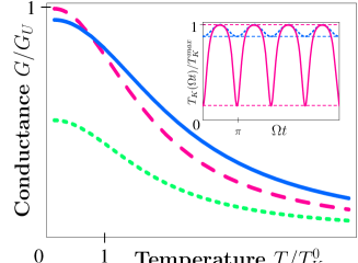
Let us first assume a temperature regime (weak coupling). In this case we can build a perturbation theory controlled by the small parameter assuming time as an external parameter. The series of perturbation theory can be summed up by means of a renormalization group procedure Hewson . As a result, the Kondo temperature becomes oscillating in time:
| (25) |
Neglecting the weak time-dependence of the effective bandwidth , we arrive at the following expression for the time-averaged Kondo temperature:
| (26) |
Here denotes averaging over the period of the mechanical oscillation. The expression (26) acquires an especially transparent form when the amplitude of the mechanical vibrations is small: . In this case the Kondo temperature can be written as , with the Debye-Waller-like exponent , giving rise to the enhancement of the static Kondo temperature.
The zero bias anomaly (ZBA) in the tunneling conductance is given by
| (27) |
where is a unitary conductance. Although the central position of the island is most favorable for the Breit-Wigner (BW) resonance (), it corresponds to the minimal width of the Abrikosov-Suhl resonance. The turning points correspond to the maximum of the Kondo temperature given by the equation (25) while the system is away from the BW resonance. These two competing effects lead to the effective enhancement of at high temperatures (see Fig. 12).
Summarizing, it was shown in kis06 that Kondo shuttling in a NEM-SET device increases the Kondo temperature due to the asymmetry of coupling at the turning points compared to at the central position of the island. As a result, the enhancement of the differential conductance in the weak coupling regime can be interpreted as a pre-cursor of strong electron-electron correlations appearing due to formation of the Kondo cloud.
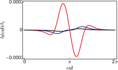
Let us consider now the strong coupling regime, . The current through the system subject to a constant source-drain bias can be separated in two parts: a dc current associated with a time-dependent dc conductance and an ac current related to the periodic motion of the shuttle. For both currents Kondo physics plays an important role. While the dc current is mostly responsible for the frequency shift, the ac current gives an access to the dynamics of the Kondo cloud and provides information about the kinetics of its formation. In order to evaluate both contributions to the total current we rotate the electronic states in the leads in such a way that only one combination of the wave functions is coupled to the quantum impurity. The cotunneling Hamiltonian may be rationalized by means of the Glazman-Raikh rotation, parametrized by the angle defined by the relation .
Both the ac and dc contributions to the current can be calculated by using Nozière’s Fermi-liquid theory (see Nozieres74 for details). The ac contribution, associated with the time dependence of the Friedel phase kis12 , is given by
| (28) |
() and the “ohmic" dc contribution is fully defined by the adiabatic time-dependence of the Glazman-Raikh angle
| (29) |
As a result, the ac contribution to the total current can be considered as a first non-adiabatic correction:
| (30) |
where and is the Kondo temperature at the equilibrium position. The small correction to the adiabatic current in (30) may be considered as a first term in the expansion over the small non adiabatic parameter , where is the retardation time associated with the inertia of the Kondo cloud. Using such an interpretation one gets .
Equation (30) allows one to obtain information about the dynamics of the Kondo clouds from an analysis of an experimental investigation of the mechanical vibrations. The retardation time associated with the dynamics of the Kondo cloud is parametrically large compared with the time of formation of the Kondo cloud and can be measured owing to a small deviation from adiabaticity. Also we would like to emphasize a supersensitivity of the quality factor to a change of the equilibrium position of the shuttle characterized by the parameter (see Fig. 13). The influence of strong coupling between mechanical and electronic degrees of freedom on the mechanical quality factor has been considered in kis12 . It has been shown that both suppression and enhancement of the dissipation of nanomechanical vibrations (depending on external parameters and the equilibrium position of the shuttle) can be stimulated by Kondo tunneling. The latter case demonstrates the potential for a Kondo induced electromechanical instability.
Summarizing, we emphasize that the Kondo phenomenon in single electron tunneling gives a very promising and efficient mechanism for electromechanical transduction on a nanometer length scale. Measuring the nanomechanical response on Kondo-transport in a nanomechanical single-electron device enables one to study the kinetics of the formation of Kondo-screening and offers a new approach for studying nonequilibrium Kondo phenomena. The Kondo effect provides a possibility for super high tunability of the mechanical dissipation as well as super sensitive detection of mechanical displacement.
V Experimental observation of electron shuttling
Electron shuttling was theoretically predicted to occur in mechanically soft mesoscopic systems about 15 year ago shuttleprl . Since then there has been a steadily increasing interest in studying this nonequilibrium electromechanical phenomenon from both theoretical and experimental points of view. Each year the technical capability to fabricate shuttle-like devices improves. On the experimental side there are two main directions in the study of mechanically mediated electron transport: (i) electron shuttling in NEMS with intrinsic electromechanical coupling, and (ii) electron transfer caused by an external excitation of mechanical motion. Here we briefly review several recent publications, which have claimed to observe electron shuttling. We start with the nanoelectromechanical devices based on vibrating cantilevers.
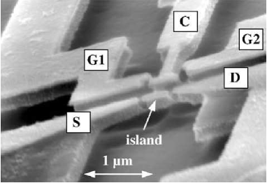
Externally driven nanomechanical shuttles have been designed in Refs. erbe1, ; erbe, . In these experiments a nanomechanical pendulum was fabricated on a Si-on-insulator substrate using electron and optical lithography. A metal island was placed on a clapper, which could vibrate between source and drain electrodes (see Fig. 14). The pendulum was excited by applying an ac voltage between two gates on the left- and right-hand sides of the clapper. The observed tunneling source-drain current was strongly dependent on the frequency of the exciting signal having pronounced maxima at the eigenfrequencies of the mechanical modes. This fact signalizes a shuttling mechanism of electron transfer at typical shuttle frequencies of about 100 MHz. The measured average dc current at 4.2 K corresponds to electrons per cycle of mechanical motion. Both a theoretical analysis and numerical simulations showed that a large portion of the voltage also acts on the island.
A very important modification of the setup in Fig. 14 was presented in Ref. sheibe, . There a silicon cantilever is part of a mechanical system of coupled resonators, which is a construction that makes it possible to drive the shuttle mechanically with a minimal destructive influence from the actuation dynamics on the shuttle itself. This is achieved by a clever design that minimizes the electrical coupling between the driving part of the device (either a magnetomotively driven, doubly clamped beam resonator, or a capacitively coupled remote cantilever) and the driven part (the cantilever that carries the shuttle on its tip). In principle, systems of this type can be used for studies of shuttle transport through superconducting and magnetic systems.
In Ref. beam, the role of nanocantilever was played by a semiconductor nanowire. In was shown that under certain conditions the constant electron beam produced by a scanning electron microscope can excite self-sustained mechanical oscillations of semiconducting SiC nanowire. The nanowire plays the role of mechanical resonator and may be represented by an circuit element (where is the nanowire resistance and is the capacitance between the nanowire end and its environment or some electrode placed near the resonator). The periodic electrostatic force, which depends on the charge of the wire, acts on the wire due to variations in capacitance. The charge on the nanowire is also a time-dependent function. Discharging occurs due to relaxation accompanied by the drift of electrons to the tungsten tip, on which the wire is attached. The charging is provided by the electron beam (for details see beam ). The semiconductor nanowire starts to oscillate and goes to the stationary cycle. Thus in beam a new type of electromechanical coupling was studied.
Interesting results on mechanically assisted charge transfer were obtained in Ref. nm, for a device fabricated as a silicon nanopillar located between source and drain contacts (see Fig. 15). The device was manufactured in a two step process: nanoscale lithography using a scanning electron microscope (SEM) and, second, dry etching in a fluorine reactive ion etcher (RIE). The lithographically defined gold structure acts both as electrical current leads and etch mask for the RIE. A simple geometry defined by SEM consequently results in the freestanding isolating nanopillar of intrinsic silicon with a conducting metal (Au) island at its top (see Fig. 15). This island serves as the charge shuttle. The metal island and the nanopillar are placed in the center of two facing electrodes. The system is biased by an ac voltage at source, rather than a sole dc bias, to avoid the dc-self excitation. Application of an ac-signal excites one of the nanopillar eigenmodes resonantly. The device was operated at room temperature and the capacitance was not sufficiently small to realize the Coulomb blockade regime. The dependencies of the current on bias frequency, as well as on an additional dc bias, allowing to tune resonances, were measured.
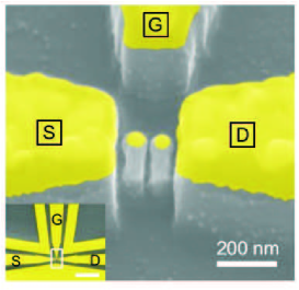
In Refs. kim2, and kim, electron transport at room temperature through two nanopillars was considered. The nanopillars act as shuttles placed in series between source and drain electrodes under ac/dc excitation (see Fig. 16). The linear size of the island on top of each pillar was 65 nm with pillar heights of 250 nm and an inter-pillar distance of 17 nm. At first the I-V characteristics at room temperature were measured kim without any ac signal. The bias voltage dependence of the current was shown to be almost linear (except for a small deviation above 1 V). At low voltages ( mV) Coulomb blockade features (a CB staircase) are apparent. From experimental data one finds the charging energy of the two coupled nanopillars to be meV, which is larger than the (room) temperature equivalent of the experimental setup.
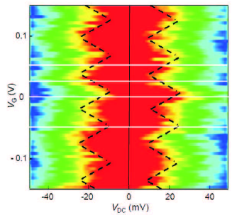
The dependence of current on gate and bias voltages is manifested in the Coulomb diamonds (see Fig. 17) in agreement with theoretical calculations. Here the typical Coulomb blockade staircase (superimposed on an ohmic response) is smeared due to thermal broadening and shuttling effects.
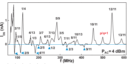
Then, a radio frequency signal (1 MHz - 1 GHz) was fed without any dc bias added. Due to the alternating-voltage induced ac current one would expect a zero-average (over an ac period) dc current without the mechanical subsystem However, in the considered experiment a nonzero net current was observed. The authors explained this fact by the excitation of a mechanical motion of the nanopillars. The effect of current rectification indicates a dynamical violation of P-symmetry (symmetry with respect to coordinates reflection ) in the system. The direction and the amplitude of the dc current depends on the ac frequency (see Fig. 18). The presence of a broad set of resonances indicates the existence of different mechanical modes of the coupled nanopillars (Fig. 18).
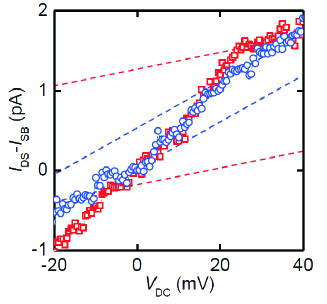
Different mechanical modes were investigated by applying a low dc bias voltage. The observed I-V characteristics (with the zero-bias current subtracted) is plotted in Fig. 20. The step-like features in the current-voltage dependence can be interpreted kim as a signature of electron shuttling in the Coulomb blockade regime.
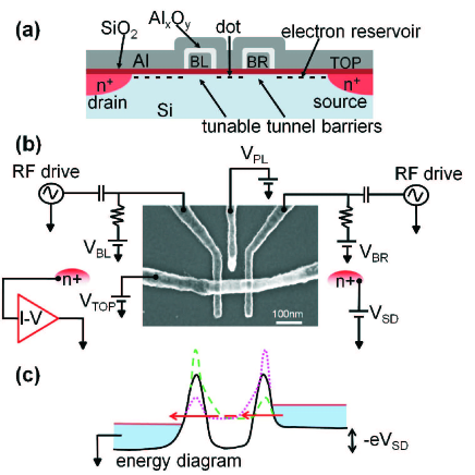
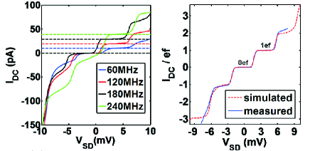
Another trend in the study of electron shuttles is to mimic shuttling effects by time dependent tunneling barriers. The authors of Ref. Chan, investigated single-electron “shuttling" with a silicon metal-oxide-semiconductor quantum dot at low temperature (300 mK). The analyzed system represents an electron layer at a Si/SiO2 interface below an aluminium top gate. This layer forms a conduction channel between source and drain electrodes (see Fig. 19). The quantum dot is formed by two additional gates, which produce tunnel barriers. The effects of mechanical degrees of freedom of the quantum dots are mimicked here by an ac voltage of frequency applied to both gates. Periodic variations of the barrier heights induce periodic effective “displacements" of the quantum dot on the nanometer scale. Fig. 21 demonstrates the dependence of the current on the bias voltage for different frequencies, . The observed results can be explained by a sequential tunneling model with the electron temperature is a fitting parameter. Electrons are “hotter" than the environment due to ac voltage heating.
An elegant experiment was performed by Park et al. park , who studied electron transport through a fullerene molecule placed in the gap between two gold electrodes. The experimental results (a stair-case-like dependence of current on bias voltage) are well explained by the process of vibron-assisted tunneling braigflens . The shuttle model was also used for an explanation of the step-like features on I-V characteristics (see the discussion in reviews shuttlerev1 ; shuttlerev2 ).
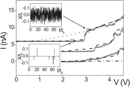
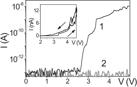
In Ref. Moskalenko, the authors reported shuttling by a 20 nm gold particle pasted into the gap (10-20 nm) between two electrodes and attached to them through a monolayer of organic molecules (1.8 octanedithiol). Experimental I-V characteristics are presented in Fig. 22. One can see that the theoretical fit using shuttle model is in a good agreement with experiment. At low voltages the current through the device is absent (the nanoparticle is in a locked state). At high voltages the nanoparticle begins to vibrate (the quantum dot escapes from the locked state), because more electrons are transferred to the granule and the electrostatic force acting on it becomes strong enough to de-pin the shuttle. The onset of shuttle instability occurs at higher bias voltages than predicted by a theory assuming frictionless shuttle motion. This discrepancy can be explained by the binding of the particle to the electrodes (respectively the value of the threshold voltage is increased). Experimental data in favor of this assumption is the observation of an I-V hysteresis loop (see Fig. 23). Without a gold particle the current through the device is determined by the sequential tunneling of electrons. Comparison of the experimental data and theoretical calculations suggests that the average number of electrons that are involved in the shuttling at voltages of order 3 V is about 20. This experiment can be interpreted as electron shuttling but the device is operated in a regime very far from single electron tunneling (Coulomb blockade regime). Is it possible to fabricate a shuttle-like device operated in the Coulomb blockade regime by dc bias voltage? Although this shuttle was not observed yet, the “road" to its discovery now is sufficiently clear.
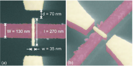
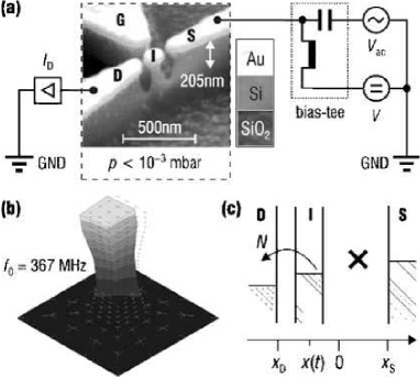
In Ref. self, the authors claimed to have found a charge shuttle (by the observation of sustained self-oscillation) operated solely by an applied dc voltage without external actuation. The island of the shuttle device in Ref. self, is a gold particle with typical dimensions 35 nm270 nm40 nm, placed at the center of a suspended silicon nitride string (see Fig. 24). Experiments were performed in helium exchange gas with a pressure of 0.5 mbar in a helium dewar at K. Forty-four samples were studied for statistical processing. To observe voltage-sustained self-oscillations the resonant acoustic drive is turned off when the island is charged. After that the stable charge transport is observed for almost 2000 s (about shuttle cycles). The reasons for the collapse of self-sustained oscillations
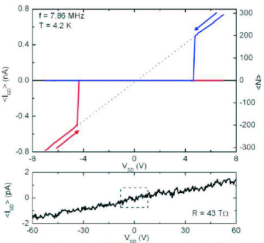
may be different: due to impact-induced coupling to out-of-plane or torsional motion or wear-induced alternation of island and electrodes, etc. In the absence of mechanical shuttling the current is a linear function of bias voltage (see Fig. 25). The presence of electron shuttling is indicated by a step-like current dependence. The average number of transferred electrons () is easily found from the I-V characteristics (see Fig. 25). The advantage of the dc-biased self-sustained shuttle current is the significant drop of external heat load on the system. The described experiment opens the pathway to observe a Coulomb blockade shuttle operated solely by a dc bias.
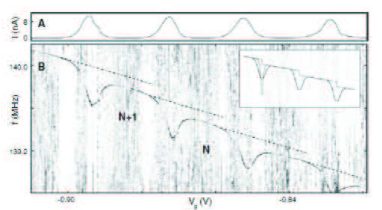
One of the most promising objects to be used for observing electron shuttling is a suspended carbon nanotube. To observe an electron shuttle it is important to fabricate an electromechanical system with two properties: (i) a soft mode of mechanical vibrations that is susceptible to becoming unstable when a bias voltage is applied, and (ii) a sufficiently strong electromechanical coupling that can overcome mechanical damping. In devices based on suspended carbon nanotubes both these conditions are realized sapmaz ; der . Three different vibrational modes (the radial mode , the stretching mode and the bending mode , is the nanotube length) can be excited in transport experiments with suspended carbon nanotubes. Recently it was shown that in a suspended carbon nanotube actuated by rf-radiation, the mechanical subsystem is sensitive to single-electron transport der (see Fig. 26). In Ref. der, the influence of a gate voltage on the frequency of vibrational modes in the Coulomb blockade regime of electron transport was studied. The bending mode was excited by radiation of a nearby rf antenna at the resonance frequency. This frequency was shown to drop at bias voltages such that the Coulomb blockade is lifted and an additional electron is transferred through the nanotube. The experiment demonstrates strong electromechanical coupling in suspended carbon nanotubes.
VI Conclusions
This review demonstrates that during the last several years there has been significant activity in the study of nanoelectromechanical (NEM) shuttle structures. New physics was harvested for theoretical suggestions of how to achieve new functionality of shuttle devices. A short list of these suggestions would include the following items:
1) The polaronic approach for studying nanoelectromechanics beyond the limit of weak NEM coupling was developed. This approach, resulting in a qualitative modification of the voltage and temperature control on NEM performance, could be applied to molecular-based shuttle devices known for their high mechanical deformability. 2) New NEM phenomena are possible in superconducting shuttle devices. The superconducting current through Josephson weak links supported by Andreev bound states andreev (see also blom , grinzwajg ) is qualitatively modified by coupling the latter to nanomechanical vibrations. Both mechanically assisted Cooper-pair transfer and electronically assisted cooling of a nanomechanical subsystem become possible. Strong electron-vibron interactions are manifested in the Franck-Condon blockade of the critical current () and its nonmonotonous (anomalous) temperature behavior. 3) The possibility to achieve an external control on the direction of energy transfer between electronic and mechanical subsystems has been demonstrated. Efficient ground state cooling of a nanomechanical resonator was predicted in both superconducting and non-superconducting NEM-SET systems cooling ; coolsantandrea . 4) The role of the electronic spin is important in shuttle devices made of magnetic materials. Spin-dependent exchange forces can be responsible for a qualitatively new nanomechanical performance opening a new field of study that can be called spintro-mechanics. 5) Electronic many-body effects, appearing beyond the weak tunneling approach, result in single electron shuttling assisted by Kondo-resonance electronic states. The possibility to achieve a high sensitivity to coordinate displacement in electromechanical transduction along with the possibility to study the kinetics of the formation of many-body Kondo states has also been demonstrated recently.
There are still a number of unexplored shuttling regimes and systems, which one could focus on in the nearest future. In addition to magnetic and superconducting shuttle devices one could explore hybrid structures where the source/drain and gate electrodes are hybrids of magnetic and superconducting materials. Then one could expect spintromechanical actions of a supercurrent flow as well as superconducting proximity effects in the spin dynamics in magnetic NEM devices. An additional direction is the study of shuttle operation under microwave radiation. In this respect microwave assisted spintromechanics is of special interest due to the possibility of microwave radiation to resonantly flip electronic spins. As in ballistic point contacts grinzwajg such flips can be confined to particular locations by the choice of microwave frequency, allowing for external tuning of the spintromechanical dynamics of the shuttle. Polaronic effects in superconducting and magnetic shuttle devices represents another interesting direction for the future research. Promising nano-objects where charge shuttling could play a significant role include bio-systems. Electromechanical phenomena involving both electrons and protons could be very important for "transport" effects in cells and bacteria (see bio1 ; bio2 ; bio3 ).
Experimental studies of shuttle devices have been developed significantly during the last couple of years. A number of new implementations of the idea of nanomechanical shuttling has been suggested (see chapter V). The aim of having fully controllable mechanics of the shuttle motion in combination with the lowest possible level of dissipation motivates the modifications which have been made. The possibility to achieve mechanically controllable shuttling of a single electron was a challenge for a number of years. Evidence indicating that a Coulomb blockade shuttle device has been made was reported recently kim . Although the regime of self supported shuttle vibrations has been reached in a number of experiments (see Section 5), the observation of a shuttle instability still remains a challenge for the future. The achievements made in the technology of producing shuttle devices self give promises for the construction of magnetic and superconducting shuttle structures, which would enable one to explore a number of tempting functionalities theoretically suggested during recent years.
VII Acknowledgements
Financial support from the Swedish VR, and the Korean WCU program funded by MEST/NFR (R31-2008-000-10057-0) is gratefully acknowledged. This research was supported in part by the Project of Knowledge Innovation Progra (PKIP) of Chinese Academy of Sciences, Grant No. KJCX2.YW.W10. I. V. K. and A. V. P. acknowledge financial support from the National Academy of Science of Ukraine (grant No. 4/12-N). I. V. K. thanks the Department of Physics at the University of Gothenburg for hospitality. MK is grateful to KITP Santa Barbara for hospitality. This research was supported in part by the National Science Foundation under Grant No. NSF PHY11-25915.
References
- (1) R. I. Shekhter, Zh. Eksp. Teor. Fiz. 63, 1410 (1972) [ Sov. Phys. JETP 36, 747 (1972)]; I. O. Kulik and R. I. Shekhter, Zh. Eksp. Teor. Fiz. 68, 623 (1975) [ Sov. Phys. JETP 41, 308 (1975)]
- (2) R. I. Shekhter, Y. Galperin, L. Y. Gorelik, A. Isacsson, and M. Jonson, J. Phys.: Condens. Matter 15, R441 (2003).
- (3) R. I. Shekhter, L. Y. Gorelik, M. Jonson, Y. M. Galperin, and V. M. Vinokur, J. Compt. Theoret. Nanoscience 4, 860 (2007).
- (4) R. I. Shekhter, F. Santandrea, G. Sonne, L. Y. Gorelik, and M. Jonson, Fiz. Nizk. Temp. 35, 841 (2009) [Low Temp. Phys. 35, 662 (2009)].
- (5) M. Blencowe, Phys. Rep. 395, 159 (2004).
- (6) K. C. Schwab and M. L. Roukes, Phys. Today 58, 36 (2005).
- (7) K. L. Ekinci and M. L. Roukes, Rev. Sci. Instrum. 76, 061101 (2005).
- (8) A. N. Cleland, Foundations of Nanomechanics (Springer-Verlag, New York, 2003).
- (9) M. Poot and H. S. J. van der Zant, Phys. Rep. 511, 273 (2012).
- (10) L. Y. Gorelik, A. Isacsson, M. V. Voinova, B. Kasemo, R. I. Shekhter, and M. Jonson, Phys. Rev. Lett. 80, 4526 (1998).
- (11) L. M. Jonson, L. Y. Gorelik, R. I. Shekhter, and M. Jonson, Nano Lett. 5, 1165 (2005).
- (12) D. Fedorets, L. Y. Gorelik, R. I. Shekhter, and M. Jonson, Europhys. Lett. 58, 99 (2002).
- (13) D. Fedorets, Phys. Rev. B 68, 033106 (2003).
- (14) L. I. Glazman and R. I. Shekhter, Zh. Eksp. Teor. Fiz. 94, 292 (1988) [Sov. Phys. JETP 67, 163 (1988)].
- (15) N. S. Wingreen, K. W. Jacobsen, and J. W. Wilkins, Phys. Rev. B 40, 11834 (1989).
- (16) J. Koch, and F. von Oppen Phys. Rev. Lett. 94, 206804 (2005); J. Koch, F. von Oppen, and A. V. Andreev, Phys. Rev. B 74, 205438 (2006) .
- (17) M. Galperin, M. A. Ratner, and A. Nitzan, J. Phys.: Cond. Matter 19, 103201 (2007).
- (18) I. V. Krive, A. Palevski, R. I. Shekhter, and M. Jonson, Fiz. Nizk. Temp. 36, 155 (2010) [Low Temp. Phys. 36, 119 (2010)].
- (19) G. A. Skorobagat’ko, I. V. Krive, and R. I. Shekhter, Fiz. Nizk. Temp. 35, 1221 (2009) [Low Temp. Phys. 35, No. 12 (2009)].
- (20) G. Mahan, Many-particle physics (Plenum Press, New York, 1990), p. 286.
- (21) I. G. Lang and Y. A. Firsov, Sov. Phys. JETP 16, 1301 (1963).
- (22) K. D. McCarthy, N. Prokof’ev, and M. T. Tuominen, Phys. Rev. B 67, 245415 (2003).
- (23) D. Fedorets, L. Y. Gorelik, R. I. Shekhter, and M. Jonson, in Fundamental problems of Mesoscopic Physics, edited by I. V. Lerner, B. L. Altshuler, and Y. Gefen, p. 65 (Kluwer Academic Publishers, Dordrecht, 2004).
- (24) T. Novotny, A. Donarini, and A.-P. Jauho, Phys. Rev. Lett. 90, 256801 (2003).
- (25) D. Fedorets, L. Y. Gorelik, R. I. Shekhter, and M. Jonson, Phys. Rev. Lett. 92, 166801 (2004).
- (26) L. Y. Gorelik, A. Isacsson, Y. M. Galperin, R. I. Shekhter, and M. Jonson, Nature 411, 454 (2001).
- (27) A. Isacsson, L. Y. Gorelik, R. I. Shekhter, Y. M. Galperin, and M. Jonson, Phys. Rev. Lett. 89, 277002 (2002).
- (28) H. van Houten, C. W. J. Beenakker, and A. A. M. Staring, in Single Charge Tunneling, edited by H. Grabert and M. H. Devoret, p. 167 (Plenum Press, New York, 1992).
- (29) P. Lafarge, P. Joyez, D. Esteve, C. Urbina, and M. H. Devoret, Phys. Rev. Lett. 70, 994 (1993).
- (30) Y. Nakamura, Yu. A. Pashkin, and J. S. Tsai, Nature 398, 786 (1999).
- (31) D. Vion, A. Aasime, A. Cottet, P. Joyez, H. Pothier, C. Urbina, D. Esteve, and M. H. Devoret, Science 296, 886 (2002).
- (32) K. Matveev, M. Gisselfält, L. I. Glazman, M. Jonson, and R. I. Shekhter, Phys. Rev. Lett. 70, 2940 (1993).
- (33) G. Wendin, and V.S. Shumeiko, Fiz. Nizk. Temp. 33, 957 (2007)[ Low Temp. Phys. 33, 724 (2007)].
- (34) Note that in spite of the degeneracy of these two charge states near either lead, the solution of the Schrödinger equation with the Hamiltonian (11) corresponds to significant fluctuations in the number of Cooper pairs on the island.
- (35) T. Novotny, A. Rossini, and K. Flensberg, Phys.Rev. B 72, 224502 (2005).
- (36) J. Skölberg, T. Löfwander, V. S. Shumeiko, and M. Fogelström, Phys. Rev. Lett. 101, 087002 (2008).
- (37) A. Zazunov, D. Feinberg, and T. Martin, Phys. Rev. Lett. 97, 196801 (2006).
- (38) I. V. Krive, R. Ferone, R. I. Shekhter, M. Jonson, P. Utko, and J. Nygard, New J. Phys. 10, 043043 (2008).
- (39) P. Utko, R. Ferone, I. V. Krive, R. I. Shekhter, M. Jonson, M. Monthioux, L. Noe, and J. Nygard, Nat. Commun. 1, 37 (2010).
- (40) A. V. Parafilo, I. V. Krive, R. I. Shekhter, and M. Jonson, (unpublished).
- (41) S. Sapmaz, P. Jarillo-Herrero, Ya. M. Blanter, C. Dekker, and H. S. J. van der Zant, Phys. Rev. Lett 96, 026801 (2006).
- (42) R. Hansen, L. P. Kouwenhoven, J. R. Petta, S. Tarucha, and L. M. K. Vandersypen, Rev. Mod. Phys. 79, 1217 (2007).
- (43) K. C. Nowak, F. H. L. Koppens, Yu. V. Nazarov, and L. M. K. Vandersypen, Science 318, 1430 (2007).
- (44) S. Foletti, H. Bluhm, D. Mahalu, V. Umansky, A. Yacoby, Nat. Phys. 318, 1430 (2007).
- (45) F. Jelezko, T. Gaebel, I. Popa, A. Gruber, and J. Wrachtrup, Phys. Rev. Lett. 92, 076401 (2004).
- (46) D. Press, T. D. Ladd, B. Zhang, and Y. Yamamoto, Nature 456, 218 (2008).
- (47) B. M. Chernobrod, G P. Berman, J. Appl. Phys. 97, 014903 (2005).
- (48) P. Rabl, S. Kolkowitz, F. Koppens, J. Harris, P. Zoller, and M. Lukin, Nat. Phys. 6, 602 (2010).
- (49) G. Balasubramanian, I. Y. Chan, R. Kolesov, M. Al-Hmoud, J. Tisler, C. Shin, C. Kim, A. Wojcik, P. R. Hemmer, A. Krueger, T. Hanke, A. Leitenstorfer, R. Bratschitsch, F. Jelezko, and J. Wrachtrup, Nature 455, 648 (2008).
- (50) J. R. Maze, P. L. Stanwix, J. S. Hodges, S. Hong, J. M. Taylor, P. Cappellaro, L. Jiang, M. V. Gurudev Dutt, E. Togan, A. S. Zibrov, A. Yacoby, R. L. Walsworth, and M. D. Lukin, Nature 455, 644 (2008).
- (51) J. M. Taylor, P. Cappellaro, L. Childress, L. Jiang, D. Budker, P. R. Hemmer, A. Yacoby, R. Walsworth, and M. D. Lukin, Nat. Phys. 4, 810 (2008).
- (52) D. Rugar, R. Budakian, H. J. Mamin, and B. W. Chui Nature 430, 329 (2004).
- (53) S. Hong, M. S. Grinolds, P. Maletinsky, R. L. Walsworth, M. D. Lukin, and A. Yacoby, Nano Lett. 12, 3920 (2012).
- (54) F. May, M. R. Wegewijs, and W. Hofstetter, Beilstein J. Nanotechnol. 2, 693 (2011).
- (55) D. A. Ruiz-Tijerina, P. S. Cornaglia, C. A. Balseiro, and S. E. Ulloa, Phys. Rev. B 86, 035437 (2012).
- (56) J. Fransson and J.-X. Zhu, Phys. Rev. B 78, 133307 (2008).
- (57) F. Reckermann, M. Leijnse, and M. R. Wegewijs, Phys. Rev. B 79, 075313 (2009).
- (58) P. Rabl, P. Cappellaro, M. V. Gurudev Dutt, L. Jiang, J. R. Maze, and M. D. Lukin Phys. Rev. B 79, 041302 (2009).
- (59) S. D. Bennett, S. Kolkowitz, Q. P. Unterreithmeier, P. Rabl, A. C. Bleszynski Jayich, J. G. E. Harris, and M. D. Lukin, arXiv: 1205.6740 (unpublished).
- (60) D. A. Garanin and E. M. Chudnovsky, Phys. Rev. X 1, 011005 (2011).
- (61) C. L. Degen, M. Poggio, H. J. Mamin, and D. Rugar, Phys. Rev. Lett. 100, 137601 (2008).
- (62) G. P. Berman, V. N. Gorshkov, D. Rugar, and V. I. Tsifrinovich, Phys. Rev. B 68, 094402 (2003).
- (63) A. Pa’lyi, P. R. Struck, M. Rudner, K. Flensberg, and G. Burkard, Phys. Rev. Lett. 108, 206811 (2012).
- (64) C. Ohm, C. Stampfer, J. Splettstoesser, and M. Wegewijs, Appl. Phys. Lett. 100,143103 (2012).
- (65) Zhao Nan, Zhou Duan-Lu, Zhu Jia-Lin Commun. Theor. Phys. 50,1457 (2008).
- (66) L. Y. Gorelik, S. I. Kulinich, R. I. Shekhter, M. Jonson, V. M. Vinokur, Phys. Rev. B71, 03527 (2005).
- (67) Colossal Magnetoresistive Oxides, edited by Y. Tokura (Gordon and Breach Science Publishers, Amsterdam, 2000).
- (68) J. Z. Sun, W. J. Gallagher, P. R. Duncombe, L. Krusin-Elbaum, R. A. Altman, A. Gupta, Yu Lu, G. Q. Gong, and Gang Xiao, Appl. Phys. Lett. 69, 3266 (1996).
- (69) J. Z. Sun, L. Krusin-Elbaum, P. R. Duncombe, A. Gupta, and R. B. Laibowitz, Appl. Phys. Lett. 70, 1769 (1997).
- (70) J. Z. Sun, Y. Y. Wang, and V. P. Dravid, Phys. Rev. B 54, R8357 (1996).
- (71) T. Kimura, Y. Tomioka, H. Kuwahara, A. Asamitsu, M. Tamura, and Y. Tokura, Science 274, 1698 (1996).
- (72) L. Y. Gorelik, S. I. Kulinich, R. I. Shekhter, M. Jonson, and V. M. Vinokur, Phys. Rev. Lett. 95,116806 (2005).
- (73) L. Y. Gorelik, S. I. Kulinich, R. I. Shekhter, M. Jonson, and V. M. Vinokur, Low Temp. Phys. 33,757 (2007).
- (74) L. Y. Gorelik, S. I. Kulinich, R. I. Shekhter, M. Jonson, and V. M. Vinokur, Appl. Phys. Lett. 90,192105 (2007).
- (75) L. Y. Gorelik, S. I. Kulinich, R. I. Shekhter, M. Jonson, and V. M. Vinokur, Phys. Rev. B 77,174304 (2008).
- (76) D. Fedorets, L. Y. Gorelik, R. I. Shekhter, and M. Jonson, Phys. Rev. Lett. 95, 057203 (2005).
- (77) L. Y. Gorelik, D. Fedorets, R. I. Shekhter, and M. Jonson, New J. Phys. 7, 242 (2005).
- (78) D. Radic, A. Nordenfelt, A. M. Kadigrobov, R. I. Shekhter, M. Jonson, and L. Y. Gorelik, Phys. Rev. Lett. 107, 236802 (2011).
- (79) G. Binash, P. Grünberg, F. Saurenbach, and W. Zinn, Phys. Rev. B 39, 4828 (1989).
- (80) E. Y. Tsymbal, O. N. Mryasov, and P. R. LeClair, J. Phys.: Condens. Matter 15, R109 (2003).
- (81) K. Tsukagoshi, B. W. Alphenaar, and H. Ago, Nature 401, 572 (1999).
- (82) R. Thamankar, S. Niyogi, B. Y. Yoo, Y. W. Rheem, N. V. Myung, R. C. Haddon, and R. K. Kawakami, Appl. Phys. Lett. 89, 033119 (2006).
- (83) R. I. Shekhter, A. Pulkin, and M Jonson, Phys. Rev. B 86, 100404 (2012).
- (84) B. Zebli, H. A. Vieyra, I. Carmeli, A. Hartschuh, J. P. Kotthaus, A. W. Holleitner, Phys. Rev. B 79, 205402 (2009).
- (85) D. W. Pang, F.-W. Yuan, Y.-C. Chang, G.-A. Li, and H.-Y. Tuan, Nanoscale 4, 4562 (2012).
- (86) L. Y. Gorelik, R. I. Shekhter, V. M. Vinokur, D. E. Feldman, V. I. Kozub, and M. Jonson, Phys. Rev. Lett. 91, 088301 (2003).
- (87) D. Goldhaber-Gordon, H. Shtrikman, D. Mahalu, D. Abush-Magder, U. Meirav, M. A. Kastner, Nature 391, 156 (1998); S. M. Cronenwett, T. H. Oosterkamp, and L. P. Kouwenhoven, Science 281, 540 (1998).
- (88) M. Pustilnik, Y. Avishai, and K. Kikoin, Phys. Rev. Lett. 84, 1756 (2000).
- (89) K. Kikoin, and Y. Avishai, Phys. Rev. Lett. 86, 2090 (2001); Phys. Rev. B 65, 115329 (2002).
- (90) M. Pustilnik and L. I. Glazman, J. Phys.: Condens. Matter 16, R513 (2004).
- (91) A. A. Abrikosov, Physics 2, 21 (1965).
- (92) H. Suhl, Physics 2, 39 (1965); Phys. Rev. 138, A515 (1965).
- (93) A. C. Hewson, The Kondo problem to Heavy Fermions, Cambridge University Press, Cambridge (1993).
- (94) D. V. Scheible, C. Weiss, J. P. Kotthaus, and R. H. Blick, Phys. Rev. Lett. 93, 186801 (2004); D. V. Scheible and R. H. Blick, Appl. Phys. Lett. 84, 4632 (2004).
- (95) A.Erbe, C. Weiss, W. Zwerger, and R. H. Blick, Phys. Rev. Lett. 87, 096106 (2001).
- (96) L. I. Glazman and M. E. Raikh, Pis’ma Zh. Eksp. Theor. Fiz. 47, 378 (1988) [JETP Lett. 47, 452 (1988)];
- (97) P. W. Brouwer, Phys.Rev. B58, R10135 (1998);P. Sharma and P. W. Brouwer, Phys. Rev. Lett. 91, 166801 (2003); T. Aono, Phys. Rev. Lett. 93, 116601 (2004).
- (98) J. R. Schrieffer and P. A. Wolf, Phys. Rev. 149, 491 (1966).
- (99) M. N. Kiselev, K. Kikoin, R. I. Shekhter, and V. M. Vinokur, Phys. Rev. B 74, 233403 (2006)
- (100) P. Nozières, J. Low Temp. Phys. 17, 31 (1974).
- (101) M. N. Kiselev, K. Kikoin, L. I. Gorelik, and R. I. Shekhter, Phys. Rev. Lett. 110, 066804 (2013).
- (102) A. Erbe, R. H. Blick, A. Tike, A. Kriele, and J. P. Kotthaus, Appl. Phys. Lett. 73, 3751 (1998).
- (103) D. V. Sheible, A. Erbe, and R. H. Blick, New J. Phys. 87, 096106 (2001).
- (104) P. Vincent, S. Perisanu, A. Ayari, M. Choueib, V. Gouttenoire, M. Bechelany, A. Brioude, D. Cornu, and S. T. Purcell, Phys. Rev. B 76, 085435 (2007).
- (105) D. V. Scheible and R. H. Blick, Appl. Phys. Lett. 84, 4632 (2004).
- (106) C. Kim, J. Park, and R. H. Blick, Phys. Rev. Lett. 105, 067204 (2010).
- (107) C. Kim, M. Prada, and R. H. Blick, ACS Nano 6, 651 (2012).
- (108) K. W. Chan, M. Möttönen, A. Kemppinen, N. S. Lai, K. Y. Tan, W. H. Lim, and A. S. Dzurak, Appl. Phys. Lett. 98, 212103 (2011).
- (109) H. Park, J. Park, A. K. L. Lim, E. H. Anderson, A. P. Alivisatos, and P. L. McEuen, Nature 407, 57 (2000).
- (110) S. Braig and K. Flensberg, Phys. Rev. B68, 205324 (2003).
- (111) A. V. Moskalenko, S. N. Gordeev, O. F. Koentjoro, P. R. Raithby, R. W. French, F. Marken, S. E. Savel’ev, Phys. Rev. B 79, 241403 (2009).
- (112) D. R. Koenig, and E.M. Weig, Appl. Phys. Lett. 101, 213111 (2012).
- (113) G. A. Steele, A. K. Huettel, B. Witkamp, M. Poot, H. B. Meerwaldt, L. P. Kouwenhoven, and H. S. J. van der Zant, Science 325, 1103 (2009).
- (114) A. F. Andreev, Sov. Phys. JETP 19, 1228 (1964); Sov. Phys. JETP 24, 1019 (1967).
- (115) H. A. Blom, A. Kadigrobov, A. Zagoskin, R. I. Shekhter, and M. Jonson, Phys. Rev. B 57, 9995 (1998).
- (116) A. Grinzwajg, L. Y. Gorelik, V. Z. Kleiner, and R. I. Shekhter, Phys. Rev. B 52, 12168 (1995).
- (117) G. Sonne, M. E. Pena-Aza, L. Y. Gorelik, R. I. Shekhter, M. Jonson, Phys. Rev. Lett. 104, 226802 (2010).
- (118) G. Sonne, M. E. Pena-Aza, L. Y. Gorelik, R. I. Shekhter, M. Jonson, Low Temp. Phys. 36, 902 (2010).
- (119) A. Yu. Smirnov, S. Savel’ev, L. G. Mourokh, and F. Nori, Phys. Rev. E 78, 031921 (2008).
- (120) A. Yu. Smirnov, S. Savel’ev, and F. Nori, Phys. Rev. E 80, 011916 (2009).
- (121) A. Yu. Smirnov, L. G. Mourokh, and F. Nori, J. Phys.: Condens. Matter 23, 234101 (2011).