Design principles for HgTe based Topological Insulator Devices
Abstract
The topological insulator properties of CdTe/HgTe/CdTe quantum wells are theoretically studied. The CdTe/HgTe/CdTe quantum well behaves as a topological insulator beyond a critical well width dimension. It is shown that if the barrier(CdTe) and well-region(HgTe) are altered by replacing them with the alloy CdxHg1-xTe of various stoichiometries, the critical width can be changed.The critical quantum well width is shown to depend on temperature, applied stress, growth directions and external electric fields. Based on these results, a novel device concept is proposed that allows to switch between a normal semiconducting and topological insulator state through application of moderate external electric fields.
I Introduction
An insulator is conventionally defined as a material that does not conduct electricity. In most insulators the lack of electric conduction is explained using its bandstructure properties.The band theory predicts that an insulator has an energy gap separating the conduction and valence bands. As a result of this finite band-gap there are no electronic states to support the flow of current. Recently, materials that have an energy gap in bulk but possess gapless states bound to the sample surface or edge have been theoretically predicted and experimentally observed. Hasan and Kane (2010) These states, in a time reversal invariant system are protected against perturbation and nonmagnetic disorder. Fu and Kane (2007); Roy (2009); Kane and Mele (2005); Murakami (2007) Materials that support such states are known as topological insulators (TI). Examples of materials with such properties include Bi2Te3, Bi2Se3, BixSb1-x alloys, and CdTe/HgTe/CdTe quantum wells. Bi2Te3,Bi2Se3, and BixSb1-x belong to the class of 3-D topological insulators (3D-TI) and host bound states on their surface. Zhang et al. (2009); Xia et al. (2009); Chen et al. (2009) CdTe-HgTe-CdTe quantum wells, which were the first predicted TIs are 2-D topological insulators (2-D TI). Unlike their 3D counterpart, they possess bound states at the edge of the quantum well. König et al. (2007); Bernevig et al. (2006); Roth et al. (2009) These conducting surface and edge states develop at the boundary between two insulators, where one is normal (NI) and the other of inverted band ordering. The surface states, which are subject to the details of the band properties of each involved material can mutually influence each other. It is therefore essential to theoretically study the surface states under various conditions.
This work proposes ways that can efficiently invert the band profile of a CdTe/HgTe/CdTe heterostructure and create bound edge states. Specifically, the transition from an NI to a TI through external adiabatic parameters, adjustable lattice constants, or modulation of the electron-hole band coupling is the underlying theme. The paper is organized as follows: In Section II, details of the CdTe/HgTe/CdTe structure and method to compute the energy dispersion are described. Section III discusses various inverted band structures, device and material conditions that can lead to topologically protected conducting surface states. The concept of creating a switch from a topological insulator is developed here. The key results discussed in the paper are summarized in Section IV.
II Materials and Methods
An HgTe quantum well flanked by CdTe barriers has been shown to have edge states with topological insulator properties. Büttiker (2009) TI behaviour is possible because CdTe is a normal insulator and is placed in contact with an inverted insulator HgTe. A representative sketch of the device is shown in Fig.1. CdTe is a wide band gap semiconductor () with positive energy gap (NI) and a small lattice mismatch of 0.5% with HgTe. CdTe, because of similar lattice constants is chosen as the barrier for the HgTe well region though in principle any normal ordered material would suffice. The normal valence and conduction band are reversed in their energetic order in HgTe as indicated in Fig. 1 and explained in the next paragraph.
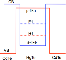
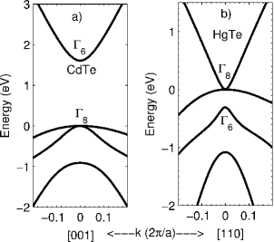
The inversion of bands for the CdTe/HgTe/CdTe heterostructure is achieved through the HgTe component. Both CdTe and HgTe belong to the zinc blende (ZB) structure with Td point group symmetry. The highest valence and lowest conduction band is made up of p and s orbitals respectively. A normal band order at has lowest conduction band () with symmetry above the top of the valence bands () with symmetry. The state has s-type symmetry and the state has p-type symmetry. In a normal ordered material state is energetically higher than the state. This order is reversed in bulk HgTe at the point due to the high spin-orbit coupling and a significant Darwin term contribution. Cade and Lee (1985) The strong spin orbit coupling pushes the valence bands upwards while the Darwin term shifts the s-type conduction band down. The Darwin term can only influence the s-type bands. Tsidil’kovskii (1982) The combined effect of spin orbit coupling and Darwin term yields an inverted band order at the point which flips the order of the high-symmetry and points for HgTe. Molenkamp The energy gap at which is defined as
| (1) |
therefore turns out to be negative for HgTe. The normal and
inverted band structures of CdTe and HgTe are illustrated in
Fig. 2(a) and Fig. 2(b) respectively.
In this work, electronic properties of the CdTe/HgTe/CdTe heterostructure are calculated within an 8-band k.p framework that includes a linear coupling between conduction and valence bands. Maciejko et al. (2011); Sengupta et al. (2011) In the calculations presented, the -axis is normal to the heterostructure and is also the confinement direction. The valence band edge , Luttinger parameters, and other related material properties are collected in Table 1. Novik et al. (2005) The boundary conditions are imposed by setting the wave function to zero at the edge of the device. Strain is added to the electronic Hamiltonian using deformation potentials defined in the Bir-Pikus method. Schulman and Chang (1986); Wu and McGill (1985)
| Material | Vso | |||||||
|---|---|---|---|---|---|---|---|---|
| CdTe | -0.27 | 5.372 | 1.671 | 1.981 | 0.11 | 1.606 | 18.8 | 0.91 |
| HgTe | 0.0 | -16.08 | -10.6 | -8.8 | -0.031 | -0.303 | 18.8 | 1.08 |
III Results and Discussion
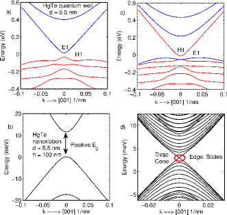
Comparison with experiment: band gap and critical widthExperiments report that a CdTe/HgTe/CdTe quantum well heterostructure with a well width under exhibits a normal band order with positive . Lu et al. (2011); Brüne et al. (2011). The calculation of the present work confirms that the conduction states at are indeed located above the valence states and the energy gap is positive (Fig. 4(a)). All band structure parameters used to reproduce the experimental observation were valid at 0 K. When the well width is exactly , a Dirac system König et al. (2008) is formed in the volume of the device (Fig. 3).
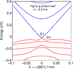
Beyond this critical well width of , the heterostructure has its bands fully inverted. The band profile has a reverse ordering of the s-type and p-type orbitals (Fig. 4(c)) and .
Accordingly, a nano-ribbon of width formed by quantizing the quantum well in its in-plane direction has a positive band gap (as shown in Fig. 4b). Similarly, a nanoribbon of width constructed out of an inverted quantum well possesses gap-less TI edge states. The band structure of this situation is illustrated in Fig. 4(d).
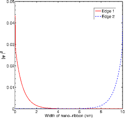
The corresponding absolute value of the squared edge-state wave functions is plotted in Fig. 5. The absolute value of the wave functions for the two edge states is maximum at the edge and gradually decay in to the bulk. This establishes that they belong exclusively to the edge states. In conclusion, the band-gap closing Dirac cone shown in Fig. 3 marks the transition from a positive band-gap to a negative one.
Band nature at finite momenta: The inversion of bands in the volume of the well is necessary for edge states with topological insulator behavior. It is important to note however, that the process of inversion happens only at the point. In the inverted dispersion plot (Fig. 4c), for momenta different from the point, the band labeled with ”H1” progresses from p to s-type. Similarly the band labeled with ”E1” changes character from s to p. Both the bands, at a finite momentum acquire atomic orbital characteristics associated with a normally ordered set of bands. TI behavior is therefore restricted to a special set of momentum points where the band structure is inverted. These set of points are collectively called the time-reversal-invariant-momentum (TRIM) points. Teo et al. (2008)
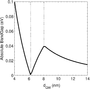
Well thickness continuously tunes the TI properties: With increasing well width, the band gap decreases continuously until the HgTe well thickness reaches (see Fig. 6). This is due to the diminishing confinement of the well’s s and p-type bands. For well thicker than , the confinement is small enough such that the inverted band ordering of HgTe is restored and the absolute value of the negative band gap is increasing (see Fig. 6).
At a HgTe well width of , the s-type band drops even below the second confined p-type state. This re-ordering of bands with well thickness is summarized in Table 2 and illustrated in Fig. 6.
| HgTe Well thickness | Highest Val.Band | Lowest Cond.Band |
|---|---|---|
| dQW dC | p-type | s-type |
| 8.2 nm dQW dC | s-type | p-type |
| dQW 8.2nm | p-type | p-type |
III.1 Stoichiometric and Temperature Control of Critical Width
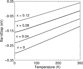
In the previous sections, it has been shown that the effective band gap of the CdTe/HgTe/CdTe quantum well depends on the confinement and consequently on the band gap difference of the well and barrier materials. Both, alloying and temperature are known to influence the effective band gap. The band gap of CdxHg1-xTe as a function of temperature Krishnamurthy et al. (1995) and stoichiometry is given by
| (2) |
A plot for the band-gap variation for the CdxHg1-xTe alloy is given in Fig. 7.
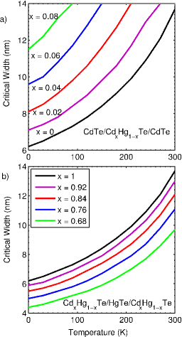
When the quantum well material of the original CdTe/HgTe/CdTe structure is substituted by CdxHg1-xTe alloy, the critical width becomes temperature and dependent. This is shown in Fig. 5 (a). Remarkably, all critical widths are equal or larger than the intrinsic critical width of . Higher concentration of CdTe in the quantum well reduces the Darwin contribution from HgTe. Therefore, the band inversion requires a wider HgTe region.
Alternatively, replacing the barrier material with CdxHg1-xTe also allows tuning the confinement and consequently the critical width. It is shown in Fig. 7(b) that this replacement yields critical widths smaller then the intrinsic if the temperature is allowed to attain values below 100 K. For a Cd molar concentration of and , the critical width dropped to . This is due to the enhanced Darwin contribution to the electronic properties with increased Hg content.
III.2 Critical widths under different growth conditions
Apart from alloy stoichiometry, the confinement also depends on the well and
barrier masses. A way to tune these effective confinement masses is by growing
the quantum well in different directions. The different masses then give
different effective well confinement and accordingly different critical
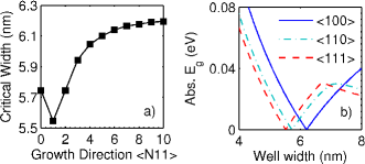
widths. This dependence is illustrated in Fig. 9. It shows the critical width of
the CdTe/HgTe/CdTe quantum well in a sequence of growth directions.
The critical widths of the and
growth directions are and respectively. Both these values are smaller than the grown quantum well critical width of .
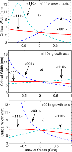
Alternatively, uniaxial stress can also tune the effective confinement masses. As representative cases, CdTe/HgTe/CdTe quantum wells were grown along , , and directions. Each quantum well was then subjected to uniaxial stress along , , and directions. Uniaxial stress along , , and was employed on three sets of CdTe/HgTe/CdTe quantum wells grown along , , and . The behaviour of the critical width for each case is shown in Fig. 10. The ideal stress orientation for each growth direction is summarized in Tables 3 and 4.
| Tensile uniaxial stress | |||
| Growth Axis | |||
| L | H | I | |
| L | H | I | |
| H | L | I | |
| Compressive uniaxial stress | |||
| Growth Axis | |||
| H | L | I | |
| H | L | I | |
| L | H | I | |
III.3 Application of an external electric field
The application of an external electric field changes the confinement and the band properties of the well states. In particular, the Rashba (structural inversion asymmetry) effect gets enhanced by electric fields in growth direction. Zhang et al. (2001) Figure 11 shows the critical width as function of the external electric field applied in the growth direction. The critical width decays with increasing field for all considered temperatures. The Rashba effect that supports the band inversion of HgTe gets increased by the electric field. Consequently, smaller well widths are required to invert the CdTe/HgTe/CdTe quantum well band structure when external electric fields are present.
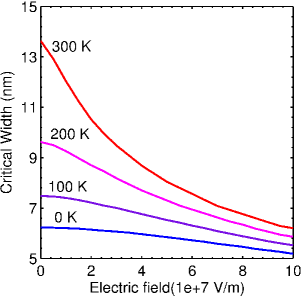
Since external electric fields can tune the critical width, the concept of a TI-switch is obvious: A CdTe/HgTe/CdTe quantum well with a well width that is close, but below the critical width can be switched by electric fields between normal and inverted band order. Such a switching band structure is expected to yield significant changes in the surface conductance, due to the unique transport properties of topological insulator states.
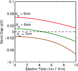
A first prototype of such a switch can be observed in Fig. 12 which shows effective band gaps of CdTe/HgTe/CdTe quantum wells for various well thicknesses under externally applied electric fields. Within the plotted range of electric field magnitude, the CdTe/HgTe/CdTe quantum well with a width of switches between normal and inverted band ordering. It is worth mentioning that this switching behavior can be observed in CdTe/HgTe/CdTe quantum wells grown in and direction.
Such topological insulator based devices under an external electric field can be employed to act as a circuit element in a fast digital environment. When the bandgap is closed and TI properties are turned on, a high Fermi velocity for the carriers, (which is an essential attribute of TIs) on surface is able to transmit an electric signal faster than a conventional inter-connect. A seamless transition from a topological insulator to normal insulator using an external electric field as demonstrated above and shown in Fig. 12 enables it to forbid an easy passage of charge/electric signal. A normal insulator with a finite band gap will behave as an open circuit element.
IV Conclusion
The present work investigates the conditions under which band inversion can occur in a CdTe/HgTe/CdTe quantum well heterostructure. It is shown that this band inversion is essential for topological insulator properties. In agreement with experimental results, it is found that the HgTe quantum well has to be thicker than to exhibit topological insulator properties. It is examined in detail how the critical width depends on various device parameters such as the growth direction, alloy stoichiometry, temperature, uniaxial stress, and external electric fields. In particular the external fields allow to switch the topological insulator properties of grown CdTe/HgTe/CdTe quantum wells. This result proposes a new class of switching devices.
References
- Hasan and Kane (2010) M. Z. Hasan and C. L. Kane, Rev. Mod. Phys. 82, 3045 (2010).
- Fu and Kane (2007) L. Fu and C. L. Kane, Phys. Rev. B 76, 045302 (2007).
- Roy (2009) R. Roy, Phys. Rev. B 79, 195322 (2009).
- Kane and Mele (2005) C. L. Kane and E. J. Mele, Phys. Rev. Lett. 95, 146802 (2005).
- Murakami (2007) S. Murakami, New Journal of Physics 9, 356 (2007).
- Zhang et al. (2009) H. Zhang, C. Liu, X. Qi, X. Dai, Z. Fang, and S. Zhang, Nature Physics 5, 438 (2009).
- Xia et al. (2009) Y. Xia, D. Qian, D. Hsieh, L. Wray, A. Pal, H. Lin, A. Bansil, D. Grauer, Y. Hor, R. Cava, et al., Nature Physics 5, 398 (2009).
- Chen et al. (2009) Y. Chen, J. Analytis, J. Chu, Z. Liu, S. Mo, X. Qi, H. Zhang, D. Lu, X. Dai, Z. Fang, et al., Science 325, 178 (2009).
- König et al. (2007) M. König, S. Wiedmann, C. Brüne, A. Roth, H. Buhmann, L. Molenkamp, X. Qi, and S. Zhang, Science 318, 766 (2007).
- Bernevig et al. (2006) B. Bernevig, T. Hughes, and S. Zhang, Science 314, 1757 (2006).
- Roth et al. (2009) A. Roth, C. Brüne, H. Buhmann, L. Molenkamp, J. Maciejko, X. Qi, and S. Zhang, Science 325, 294 (2009).
- Büttiker (2009) M. Büttiker, Science 325, 278 (2009).
- Cade and Lee (1985) N. Cade and P. Lee, Solid state communications 56, 637 (1985).
- Tsidil’kovskii (1982) I. Tsidil’kovskii, Band Structure of Semiconductors (Pergamon Press, 1982), ISBN 9780080216577.
- (15) L. Molenkamp, (Private Communication).
- Maciejko et al. (2011) J. Maciejko, T. Hughes, and S. Zhang, Annu. Rev. Condens. Matter Phys. 2, 31 (2011).
- Sengupta et al. (2011) P. Sengupta, S. Lee, S. Steiger, H. Ryu, and G. Klimeck, in MRS Proceedings (Cambridge Univ Press, 2011), vol. 1370.
- Novik et al. (2005) E. G. Novik, A. Pfeuffer-Jeschke, T. Jungwirth, V. Latussek, C. R. Becker, G. Landwehr, H. Buhmann, and L. W. Molenkamp, Phys. Rev. B 72, 035321 (2005).
- Schulman and Chang (1986) J. Schulman and Y. Chang, Physical Review B 33, 2594 (1986).
- Wu and McGill (1985) G. Wu and T. McGill, Applied Physics Letters 47, 634 (1985).
- Lu et al. (2011) J. Lu, W. Shan, H. Lu, and S. Shen, New Journal of Physics 13, 103016 (2011).
- Brüne et al. (2011) C. Brüne, A. Roth, H. Buhmann, E. Hankiewicz, L. Molenkamp, J. Maciejko, X. Qi, and S. Zhang, Arxiv preprint arXiv:1107.0585 (2011).
- König et al. (2008) M. König, H. Buhmann, L. Molenkamp, T. Hughes, C. Liu, X. Qi, and S. Zhang, Arxiv preprint arXiv:0801.0901 (2008).
- Teo et al. (2008) J. Teo, L. Fu, and C. Kane, Physical Review B 78, 045426 (2008).
- Krishnamurthy et al. (1995) S. Krishnamurthy, A. Chen, A. Sher, and M. Van Schilfgaarde, Journal of electronic materials 24, 1121 (1995).
- Zhang et al. (2001) X. Zhang, A. Pfeuffer-Jeschke, K. Ortner, V. Hock, H. Buhmann, C. Becker, and G. Landwehr, Physical Review B 63, 245305 (2001).