Observation of Asymmetric Transport in Structures with Active Nonlinearities
Abstract
A mechanism for asymmetric transport based on the interplay between the fundamental symmetries of parity () and time () with nonlinearity is presented. We experimentally demonstrate and theoretically analyze the phenomenon using a pair of coupled van der Pol oscillators, as a reference system, one with anharmonic gain and the other with complementary anharmonic loss; connected to two transmission lines. An increase of the gain/loss strength or the number of -symmetric nonlinear dimers in a chain, can increase both the asymmetry and transmittance intensities.
pacs:
05.45.-a, 42.25.Bs, 11.30.ErDirected transport is at the heart of many fundamental problems in physics. Furthermore it is of great relevance to engineering where the challenge is to design on-chip integrated devices that control energy and/or mass flows in different spatial directions. Along these lines, the creation of novel classes of integrated photonic, electronic, acoustic or thermal diodes is of great interest. Unidirectional elements constitute the basic building blocks for a variety of transport-based devices such as rectifiers, pumps, molecular switches and transistors.
The idea was originally implemented in the electronics framework, with the construction of electrical diodes that were able to rectify the current flux. This significant revolution motivated researchers to investigate the possibility of implementing this idea of ”diode action” to other areas. For example, a proposal for the creation of a thermal diode, capable of transmitting heat asymmetrically between two temperature sources, was suggested in Ref. TPC02 . Another domain of application was the propagation of acoustic pulses in granular systems NDHJ05 .
A related issue concerns the possibility of devising an optical diode which transmits light differently along opposite propagation directions. Currently, such unidirectional elements rely almost exclusively on the Faraday effect, where external magnetic fields are used to break space-time symmetry. Generally this requires materials with appreciable Verdet constants and/or large size non-reciprocal devices – typically not compatible with on-chip integration schemes or light-emitting wafers ST91 . To address these problems, alternative proposals for the creation of optical diodes have been suggested recently. Examples include optical diodes based on second harmonic generation in asymmetric waveguides GAPF01 and nonlinear photonic crystals SDBB94 , photonic quasi-crystals and molecules B08 , or asymmetric nonlinear structures LC11 . Most of these schemes, however, suffer from serious drawbacks making them unsuitable for commercial or small-scale applications. Relatively large physical sizes are often needed while absorption or direct reflection dramatically affects the functionality leading to an inadequate balance between figures of merit and optical intensities. In other cases, cumbersome structural designs are necessary to provide structural asymmetry, or the transmitted signal has different characteristics than the incident one.
In this Letter we demonstrate, experimentally and theoretically, a mechanism for asymmetric transport exploiting the co-existence of active elements with distinctive features of nonlinear dynamical systems, such as amplitude-dependent resonances. As a reference model we will use coupled nonlinear electronic Van der Pol (VDP) oscillators with anharmonic parts consisting of complementary amplifiers (gain) and dissipative conductors (loss) combined to preserve parity-time () symmetry. -symmetric structures were inspired by quantum field theories BB98 ; their technological importance was first recognized in the framework of optics MGCM08 , where several intriguing features were found MGCM08 ; GSDMVASC09 ; RMGCSK10 ; K10 ; RKGC10 ; ZCFK10 ; L09 ; L10b ; M09 ; LRKCC11 ; BFKS09 ; HRTKVKDC12 . For example, the theoretical proposal of Refs. RKGC10 ; LRKCC11 suggested using nonlinearities to induce asymmetric transport. Very recently the idea of creating -symmetric devices within the electronics framework was proposed and experimentally demonstrated in Ref. SLZEK11 . -electronics provides a platform for detailed scrutiny of many new concepts within a framework of easily accessible experimental configurations SLZEK11 ; LSEK12 ; RSEGK12 . Despite all this activity, the -symmetric Hamiltonians introduced in quantum field theory, optics, and electronics have been restricted to conservative anharmonic constituents (if any) with the matched gain and loss exclusively linear (see however the theoretical works MMK11 ).
Here, using the -electronics framework, we demonstrate with experiment, simulations, and theory, asymmetric transport from -symmetric structures that belong to this relatively unexplored class of nonlinear systems whose anharmonic parts includes the mutually matched gain and loss. Such systems, natural to the realm of electronics for which the van der Pol model was originally proposed vdp27 , can also be implemented in optics using, for example, optical amplifiers, saturable absorbers K96 and two-photon losses to realize the nonlinear -symmetry.
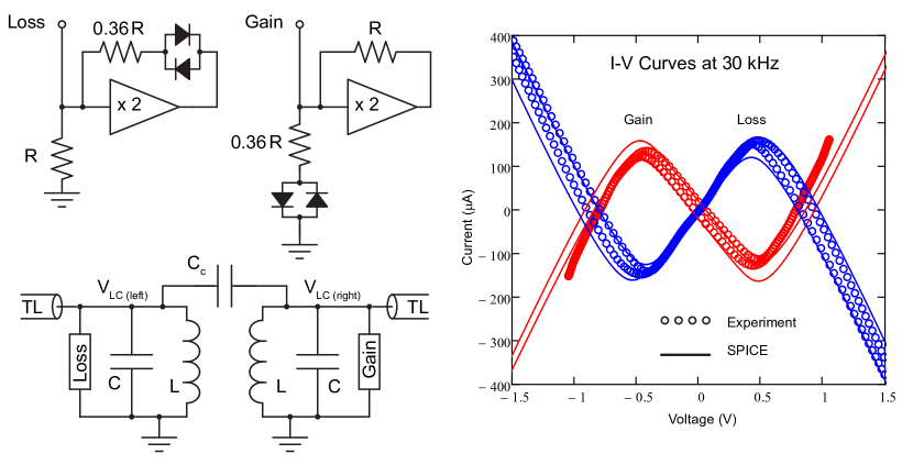
An ideal VDP oscillator has a linear anti-damping at low amplitudes which is subsequently overtaken by a cubic dissipation at high amplitudes. In electronics this is an LC oscillator in parallel with a voltage dependent conductance characterized by the I-V curve . A negative impedance converter (NIC) (upper left of Fig. 1) generates a term, and we approximate the cubic turn-around with parallel back-to-back diodes moderated by a resistor. The time-reversed conductance is constructed with the resistor and the diode combination interchanged. The resulting ”gain” and ”loss” nonlinear conductances refer to their low amplitude character. The respective nonlinear I-V curves are shown in the right panel of Fig. 1. The in series with the diodes optimizes the match to a cubic nonlinearity. It is important to note that only the parameter is used to set the gain/loss parameter , while the diode turn-on characteristics are fixed. When comparisons are made to theoretical models, the voltage scaling will consequently depend on .
The schematic of the dimer circuit is shown in the lower left of Fig. 1. The coupled heart of the circuit is identical to that used in a previous work SLZEK11 with LM356 op-amps serving in the NICs and signal buffers. The two VDP oscillators are capacitively coupled by . In principle, more complicated geometries such as chains of active nonlinear - symmetric dimers could be constructed by capacitively coupling additional dimers into the desired topology. The experimental measurements of this work are limited to the dimer as a check on SPICE simulations used for larger systems.
Transmission lines (TL) with impedance are attached to the left (lossy) and the right (gain) nodes of the dimer to complete the scattering system used to perform our transport measurements. Experimentally, these take the form of resistances in series with independent voltage sources, here HP3325A synthesizers, on the right and left sides. The incoming and outgoing traveling wave components associated with a particular TL are deduced from the complex voltages on both ends of , as sampled by a Tektronix DPO2014 oscilloscope. For example, on the left (lossy) side, with the voltage amplitude on the circuit node, and the voltage amplitude on the synthesizer side of the coupling resistor , the incident wave on the dimer has a voltage amplitude and the outgoing wave has a voltage amplitude . An equivalent relation holds for the right TL terminal with the superscripts interchanged, since they refer to right or left wave traveling direction regardless of the terminal orientation.
The scattering measurements are performed for fixed incoming wave amplitude set by of the signal generator on either the left or the right side with the other side set to zero. The generator frequency is stepped (up or down), and the three relevant waveforms, and on the left and right are simultaneously captured (the channel on the transmitted side is zero). Harmonic components of each wave constituent can be independently analyzed for magnitude, and relative phase. Instrumentation noise and sample time determine the accuracy of this analysis, which was found to be .
Circuit behavior was numerically modeled by the NGSPICE simulator ngspice . Modern simulation goes beyond a lumped element approach, in which circuits can only be modeled by idealized passive component approximations. Rather, behavioral modeling focuses on the mathematical relations between inputs, parameters, and outputs of a complicated nonlinear component; often by incorporating virtual dependent sources into the resulting model. This allows for faster speed and higher accuracy in calculations of circuit behavior. Most manufacturers, in fact, provide ready-made behavioral models for their devices. Here, for the LF356 op-amp we heavily utilized Texas Instruments’ modified Boyle model, as well as the parametrized diode model of Fairchild’s 1N914 model_src .
In Fig.1, circuit analysis was done in the time-domain for each individual element (gain or loss circuit) of the nonlinear -symmetric dimer. Using initial DC operating conditions, a frequency-dependent source drives a circuit through a transient regime into steady-state operation, at which point the voltages and currents are recorded. The measured I-V response curve (see Fig. 1) is reproduced by the simulations.
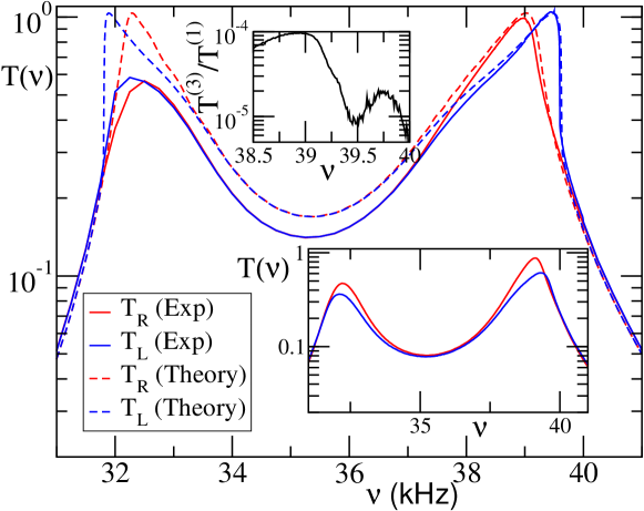
For the transmittances versus the driving frequency in Fig.2, the steady-state time-domain simulations of the -symmetric dimer in the scattering configuration are similarly obtained. Fourier analysis is used to extract the relevant frequency-dependent voltages and currents, which are then used to calculate the scattering parameters. As a check of the accuracy of our numerical approach, we have also extracted the transmittance using a nonlinear harmonic balance circuit analysis hb_footnote . We have confirmed that the results are identical, within numerical accuracy, to the ones obtained from the time-domain analysis. In Fig. 2 we also report the experimental left and right transmittances for the -symmetric VDP dimer. The overall shape of the measured transmittances reasonably match the numerical simulations. The deviations are likely associated with a small parasitic inductive coupling.
A striking feature of the results of Fig. 2 is the fact that the transmittance from left to right differs from the transmittance from right to left , i.e. . The phenomenon is more pronounced closer to the resonance frequencies of the corresponding linear problem and is the main result of this paper. This asymmetry is forbidden by the reciprocity theorem in the case of linear, time-reversal symmetric systems. In fact, it is not present even in the case of linear -symmetric structures LSEK12 , although the time-reversal symmetry in this case is also broken. At the same time, a Hamiltonian nonlinear medium by itself cannot generate such transport asymmetries. Furthermore, we find that increasing the gain/loss parameter which is responsible for the asymmetric transport, maintains or even enhances the transmitted intensities (compare the lower inset of Fig. 2 with the main panel). This has to be contrasted with other proposals of asymmetric transport (see for example Ref. LC11 ) where increase of asymmetry always leads to reduced transmittances.
We have also developed a theoretical understanding of asymmetric transport by restricting our analysis to the basic harmonic. This approximation is justified by our measurements which indicate that the main part of the transmitted power is concentrated in the fundamental harmonic. An example is shown in the upper inset of Fig. 2 where we report the ratio between transmittances of the third harmonic to the fundamental. Even harmonics are absent in the transmission spectra due to the nature of VDP anharmonicity, while for higher harmonics the experimental values of are below the noise level of our measurements.
Application of the first and second Kirchoff’s laws at the TL-dimer contacts allow us to find the current/voltage wave amplitudes at the left (L) and right (R) contact. We get
| (1) | |||
where the dimensionless current/voltage amplitudes at the lead-dimer contacts are defined as , . The dimensionless time is and is the dimensionless TL conductance, while we have also introduced the dimensionless capacitance , a measure of the intra-dimer coupling.
At any point along a TL, the current and voltage determine the amplitudes of the right and left traveling wave components. The forward and backward wave amplitudes, and the voltage and current at the TL-dimer contacts satisfy the continuity relation
| (2) | |||||
Note that Eqs. (1) contains nonlinear terms on the r.h.s. which are responsible for harmonic generation. However, as suggested by the experimental data, we can neglect these higher harmonics and thus restrict our analytic study to the fundamental. Keeping this in mind when substituting Eqs. (2) into Eqs. (1), we get
| (3) |
where we used the compact notation for and . The exponent above takes the values for current amplitudes respectively.
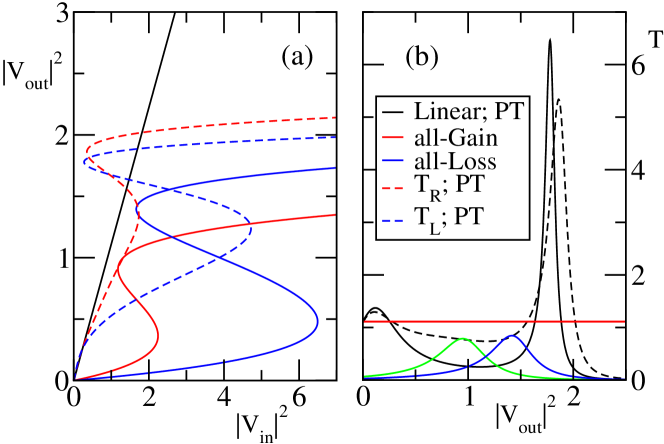
The way to solve Eqs. (3) is to introduce the backward transfer map TH99 . The latter uses the output amplitude as an initial condition together with the boundary conditions () for a left (right) incoming wave. Iterating backwards, we calculate the corresponding incident () and reflected () amplitudes for a left (right) incident wave. Representative curves are shown in Fig. 3a. The associated transmittances are defined as . Straightforward algebra gives:
| (4) |
where . The transmittance for a right incident wave is given by the same expression as Eq. (4) with the substitution of i.e. . The origin of the latter inequality is due to the fact that nonlinear resonances are detuned differently for left and right incident waves, as seen from Eq. (4) (compare black dashed and solid lines in Fig. 3b). The case corresponds to a linear passive dimer for which in agreement with Eq. (4). To further highlight the importance of the interplay between nonlinearity and -symmetry, we also report in Fig. 3 the transmittances for a nonlinear VDP dimer with both elements having gain or loss and for a linear -symmetric dimer. In contrast to the nonlinear -symmetric structure, the transmission is symmetric.
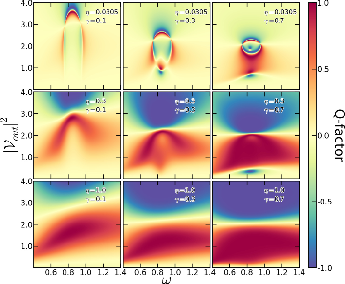
Since the phenomenon is nonlinear the asymmetry depends on both frequency and amplitude. To quantify its efficiency, in Fig. 4 we report the rectification factor
| (5) |
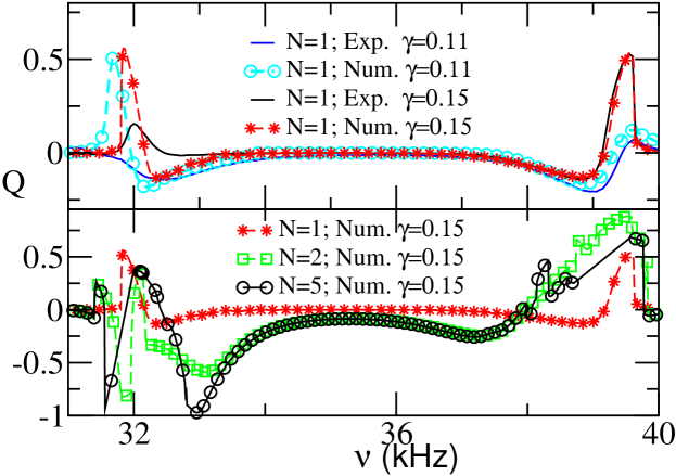
which approaches for maximal asymmetry. Note that increasing broadens the regions in which is relatively large. Some representative experimental rectification factors for a single dimer and two different values of are shown in Fig. 5 together with the SPICE simulations. The measurements and the simulations compare nicely with one another and are in agreement with the theoretical calculations shown in Fig. 4. Furthermore, increasing the number of nonlinear -symmetric dimers leads to a considerable increase of the -factor. This can be seen in Fig. 5 even for the case of . Although this behavior can be formally analyzed by evaluating the order backward transfer map, a qualitative explanation can be provided based on our understanding of the dimer. Specifically, one expects that the increase of the number of -symmetric dimers introduces nonlinear resonances (which are detuned differently for left and right incoming waves), thus broadening the frequency domain for which asymmetric transport is present.
Conclusions - Using coupled -symmetric VDP oscillators, we have demonstrated experimentally and theoretically a mechanism based on the co-existence of nonlinearity and -symmetry which leads to asymmetric wave transport. Unlike the linear or passive nonlinear cases, this is achieved concurrent with a significant level of transmittance. These findings can be applied to photonic or phononic systems as a guide for optimizing design in order to achieve maximal asymmetry.
Acknowledgments – This research was supported by an AFOSR grant No. FA 9550-10-1-0433, and by an NSF ECCS-1128571 grant. NB&SF acknowledge support from Wesleyan Faculty/Student Internship grants.
References
- (1) M. Terraneo, M. Peyrard, G. Casati, Phys. Rev. Lett. 88, 094302 (2002); D. Segal, A. Nitzan, ibid. 94, 034301 (2005); C. W. Chang et al., Science 314 1121 (2006).
- (2) V. F. Nesterenko et al., Phys. Rev. Lett. 95, 158702 (2005).
- (3) B. E. A. Saleh and M. C. Teich, Fundamentals of Photonics (Wiley, New York, 1991).
- (4) K. Gallo et al., Appl. Phys. Lett. 79, 314 (2001).
- (5) M. Scalora et al., J. Appl. Phys. 76, 2023 (1994); M. D. Tocci et al., Appl. Phys. Lett. 66, 2324 (1995).
- (6) F. Biancalana, J. of Appl. Phys. 104, 093113 (2008).
- (7) S. Lepri, G. Casati, Phys. Rev. Lett. 106, 164101 (2011)
- (8) C. M. Bender and S. Boettcher, Phys. Rev. Lett. 80, 5243 (1998); C. M. Bender, Rep. Prog. Phys. 70, 947 (2007).
- (9) K. G. Makris et al., Phys. Rev. Lett. 100, 103904 (2008); Z. H. Musslimani et al., ibid. 100, 030402 (2008).
- (10) C. E. Rüter et al., Nat. Phys. 6, 192 (2010).
- (11) A. Guo, et al., Phys. Rev. Lett. 103, 093902 (2009)
- (12) T. Kottos, Nature Physics 6, 166 (2010).
- (13) M. C. Zheng et al., Phys. Rev. A 82, 010103 (2010).
- (14) S. Longhi, Phys. Rev. Lett. 103, 123601 (2009).
- (15) A. Mostafazadeh, Phys. Rev. Lett. 102, 220402 (2009).
- (16) S. Longhi, Phys. Rev. A 82, 031801 (2010); Y. D. Chong, L. Ge, A. D. Stone, Phys. Rev. Lett. 106, 093902 (2011).
- (17) O. Bendix, et al., Phys. Rev. Lett. 103, 030402 (2009); C. T. West, T. Kottos, T. Prosen, ibid. 104, 054102 (2010).
- (18) H. Ramezani et al., Phys. Rev. A 85, 013818 (2012)
- (19) Z. Lin, et al., Phys. Rev. Lett 106, 213901 (2011).
- (20) H. Ramezani et al., Phys. Rev. A 82, 043803 (2010)
- (21) J. Schindler et al., Phys. Rev. A 84, 040101(R) (2011).
- (22) Z. Lin et al., Phys. Rev. A 85, 050101(R) (2012)
- (23) H. Ramezani et al., Phys. Rev. A 85, 062122 (2012)
- (24) A. Miroshnichenko, B. A. Malomed, Y. S. Kivshar, Phys. Rev. A 84, 012123 (2011); F. Kh. Abdullaev et al., Phys. Rev. A 83, 041805(R) (2011).
- (25) B. van der Pol, The London, Edinburgh and Dublin Phil. Mag. & J. of Sci., 2, 978 (1927).
- (26) U. Keller et al., IEEE J. Sel. Top. Quantum Electron. 2, 435 (1996).
- (27) This software is easy to use and is freely available from http://ngspice.sourceforge.net/.
- (28) SPICE models for the op-amp and diode are respectively available from http://www.ti.com/product/lf356 and http://www.fairchildsemi.com/pf/1N/1N914.html.
- (29) The nonlinear harmonic balance analysis was performed in Agilent’s proprietary Advanced Design System (ADS) 2011, using the Large Signal S-Parameter package.
- (30) G. Tsironis, D. Hennig, Phys. Rep. 307, 333 (1999); F. Delyon, Y. Lévy, B. Souillard, Phys. Rev. Lett. 57, 2010 (1986).