A single diffractive optical element for implementing spectrum-splitting and beam-concentration functions simultaneously with high diffraction efficiency∗
Jia-Sheng Yea,b, Jin-Ze Wangc, Qing-Li Huangc, Bi-Zhen Dongc, Yan Zhanga,b, and Guo-Zhen Yangc
a) Department of Physics, Capital Normal University,
Beijing 100048, P. R. China
b) Beijing Key Lab for THz Spectroscopy and Imaging, Key
Lab of THz Optoelectronics, Ministry of Education, Beijing 100048,
P. R. China
c) Institute of Physics, Chinese Academy of Sciences,
Beijing 100190, P. R. China
In this paper, a novel method is proposed, and employed to design a single diffractive optical element (DOE) for implementing spectrum-splitting and beam-concentration (SSBC) functions simultaneously. We develop an optimization algorithm, through which the SSBC DOE can be optimized within an arbitrary thickness range, according to the limitations of modern photolithography technology. Theoretical simulation results reveal that the designed SSBC DOE has a high optical focusing efficiency. It is expected that the designed SSBC DOE should have practical applications in high-efficiency solar cell systems.
Keywords:
diffractive optical element, spectrum-splitting and beam-concentration functions, thickness optimization algorithm, high optical focusing efficiency, solar cell systems
PACS: 42.15.Eq, 42.25Fx, 42.79Ek
1. Introduction
Energy and environmental problems are common challenges we are all facing in the world. Solar energy, due to its clearness and huge amount, fuels the need for the future. Nowadays, the solar energy is usually utilized through the solar cells due to the photovoltaic (PV) effect [1]. The solar cell is composed of two parts, i.e., the optical system and the cell system. The “merit” of a PV cell depends upon the manufacturing cost of the PV material as well as the cell’s efficiency.
In order to reduce the cost, the incident sunlight is often highly concentrated to offset the expensive cell [2]. An alternative way is decreasing the fabrication difficulty by using an optical system. In this case, the sunlight is spatially separated into different regions, where properly selected single junction solar cells are aligned [3]. Since cell stacking and epitaxial technologies [4] are no longer applied, it becomes much cheaper and easier.
On the other hand, for achieving a high cell efficiency, the following three main strategies are used [5]. Firstly, high efficiency converting materials such as the compounded III-IV materials are selected [6], instead of silicon. Secondly, several junctions with different bandgaps are united together from top to bottom [7], so as to break the maximum conversion efficiency of a single bandgap converter limited by the Shockley Read Hall equation [8]. However, there exist some constraints on choosing the materials and substrates due to the lattice matching problems. Thirdly, the cell efficiency may be also raised by using some new mechanism, new materials, or subwavelength structures, including local light trapping techniques [9, 10, 11, 12], plasmonics [13, 14, 15], organic solar cells [16], photonic crystals [17, 18, 19], optical waveguides [20], nano-patterned structures [21, 22, 23].
On summarizing the above two aspects of a high conversion efficiency and low cost, we can find two critical optics issues in promoting wide applications of solar cells. One is the spectrum-splitting problem, and the other is the beam-concentration problem. For implementing the spectrum-splitting function, three types of elements are usually applied, namely prisms, diffraction gratings, and dichroics. For realizing the beam-concentration function, an optical lens needs to be employed. In previous papers, these two functions are generally realized by two elements in successive steps [24, 25]. As a result, it brings about such problems as system stableness, system compactness, and alignment errors. To solve this problem, in this paper we propose to design a single diffractive optical element (DOE) that can implement spectrum-splitting and beam-concentration (SSBC) functions simultaneously. In order to make use of the modern photolithography technology in the fabrication process, an optimization algorithm is developed so that the thickness of the DOE can be confined within an arbitrary range.
This paper is organized as follows. In Section 2, the designing principle of the SSBC DOE and the thickness optimization algorithm are described in detail with formulas. In Section 3, the parameters of the designed SSBC DOEs are given, and then their performance results are presented with explanations. A conclusion is drawn in Section 4 with some discussions.
2. Designing process of the single diffractive optical element (DOE) that implements spectrum-splitting and beam-concentration (SSBC) functions simultaneously
2.1. Designing principle of the SSBC DOE
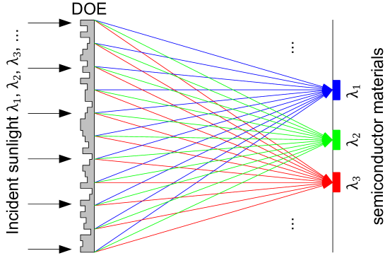
Figure 1 depicts the schematic diagram of the proposed single SSBC DOE. The sunlight is normally incident upon the front surface of the DOE on the input plane. Due to the phase modulation of its surface-relief profile, the sunlight with different wavelengths will be separately focused at their preassigned positions on the output plane, as shown in Fig. 1. If we put proper semiconductor materials at the corresponding focal positions, the solar cell conversion efficiency is expected to be significantly raised. Then, how to design such a single SSBC DOE?

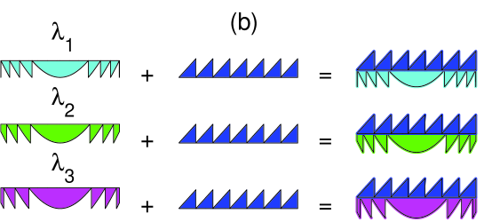
As is well known, the diffraction grating and lens can realize spectrum-splitting and beam-concentration functions, respectively. From our experience in physical optics, if we attach these two elements together, the combined element should have both functions simultaneously, as shown in Fig. 2(a). From diffractive optics, for a definite incident wavelength , the focusing refractive lens in Fig. 2(a) has a thickness function of
| (1) |
where represents the refractive index of the lens at wavelength ; stands for the horizontal coordinate with origin at the center; denotes the preset focal length. For the spectrum-splitting grating, it may be regarded as a Fresnel prism, as shown by the blue element in Fig. 2(a). Its thickness is given by
| (2) |
where means the modulus function and its value situates within for any positive real numbers and ; denotes the slope of the prism; , and is chosen as the average wavelength in the considered wavelength range. Theoretically, although the combined element can fulfill the SSBC functions, it usually has a too large thickness to fabricate because of the thick refractive lens, as shown by the red element in Fig. 2(a). Therefore, we call it as a bulk SSBC DOE, whose thickness is given by
| (3) |
In order to utilize the modern photolithography technology, the thickness of the designed SSBC DOE should be confined in a reasonable range. In physical optics, as the 2 phase can be added or removed without influencing the performance of the DOE, the refractive lens may be attenuated into a Fresnel lens while the grating part is kept unchanged. For instance, at wavelength , the thickness of the combined element after attenuation is written as
| (4) |
where , corresponding to a phase change of for wavelength ; denotes the material refractive index at wavelength . When the incident wavelength becomes , ,…, we can obtain , ,…, as shown in Fig. 2(b). So far, a new problem rises. For the solar cell system, as the incident sunlight includes multiple wavelengths, from Eq. (4), we can not get a unique boundary profile of the designed SSBC DOE.
2.2. Thickness optimization algorithm for designing the SSBC DOE
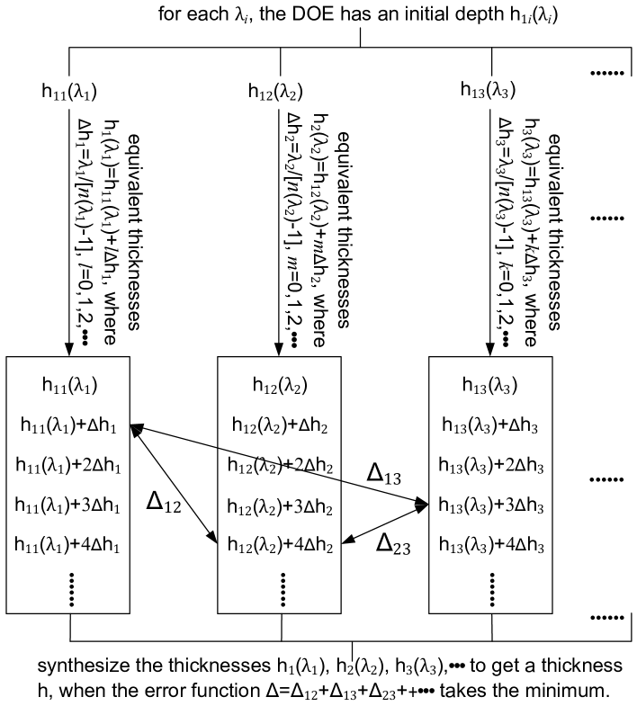
To solve the above problem, in this subsection we develop a thickness optimization algorithm. For wavelength , it has a ground thickness . Let’s assume that the largest permitted thickness of the designed DOE is , which is usually limited by the experimental fabrication conditions. Since multiples of 2 phase do not exert any impact on the DOE’s performance, a series of equivalent thicknesses may be obtained as
| (5) |
where , as shown in Fig. 3. The maximum value of is governed by . Similarly, for another incident wavelength , we obtain its corresponding series of equivalent thicknesses as
| (6) |
where ; , and represents the material refractive index at wavelength , as shown in Fig. 3. The maximum value of is determined by .
Following the above steps, for each wavelength we can generate its unique set of thicknesses. From each set, we arbitrarily select a thickness. If the total wavelength number is , altogether we will have thicknesses. Thus the error between arbitrary two thicknesses is calculated as . We define an error function as
| (7) |
Through searching the minimum value of , the optimum thickness in each set will be determined, as seen in Fig. 3. Finally, the thickness of the SSBC DOE is optimized as
| (8) |
As the thickness in Eq. (8) may take any continuous value, in the following we refer to it as . Since modern photolithographic fabrications are implemented through binary masks, the continuous DOEs are usually quantized into multilevel ones in the following way. If the maximum permitted thickness is and the total quantization level number is , each step depth is . The thickness of the quantized DOE () is derived from that of the continuous one as
| (9) |
where means taking the maximum integer no larger than a real number .
3. Performance simulation results of the designed SSBC DOEs
3.1. Designing parameters and the performance characterization
To demonstrate the validity of the proposed method, we will design the SSBC DOE and characterize its performance. Parameters are selected as follows. The incident wavelength ranges from 0.45 to 0.65. For the designing processes in Figs. 2 and 3, we choose three wavelengths as 0.45, 0.55, and 0.65. Therefore, the wavelength number in Eq. (8) is . The average wavelength is . The distance between the input plane and the output plane is . We define a length unit as . The grating angle is , therefore, the constant in Eq. (2) equals . Both the input and output planes have the same sizes of . The input and output planes are equally quantized into 4096 segments, with each element scaling about 5.18. The material of the DOE is chosen as fused silica, whose refractive index changes slightly in the visible region. Hence, we neglect the dispersive effect and assume the refractive index to be a constant as [26]. Following the above-mentioned designing procedure in Section 2, the thickness of the SSBC DOE can be obtained.
After designing the DOE, under thin-element approximation we can calculate the field distribution on the input plane (just passing through the DOE) as
| (10) |
where represents the thickness of the DOE; equals or for the bulk or the optimized SSBC DOE, respectively; denotes the transverse coordinate of the sampling point on the input plane. It is noted that the reflection losses on both interfaces of the DOE are ignored. As the propagation distance is far enough, the Fresnel diffraction integral is applied to calculating the field on the output plane as [27]
| (11) |
where represents the transverse coordinate on the output plane; denotes the Fresnel diffraction integral kernel, as given by
| (12) |
In order to characterize the performance of the DOE, the optical focusing diffraction efficiency for each wavelength is defined as
| (13) |
where denotes the geometrical transverse focal position for wavelength ; the symbol represents the magnitude of a complex number . The ultimate optical focusing diffraction efficiency of the designed SSBC DOE is averaged as
| (14) |
3.2. Performance results of the designed bulk SSBC DOE
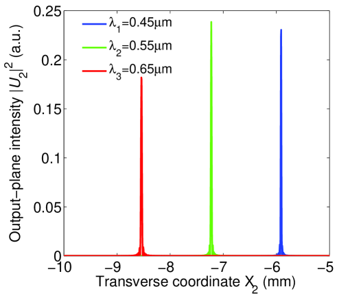
Firstly, we design the bulk SSBC DOE, which consists of the refractive lens and the diffraction grating without thickness limitation. By following the designing procedure in subsection 2.1, the thickness of the bulk SSBC DOE is evaluated. Apparently, on ignoring the material dispersive effect, the boundary of the bulk SSBC DOE does not depend on the designing wavelength. Therefore, it suits all the designed wavelengths well and is expected to have very good performance. Through calculating the Fresnel diffraction integral, the intensity distributions on the output plane are obtained and displayed in Fig. 4. The blue, green, and red curves correspond to the intensity distributions for incident wavelengths of 0.45, 0.55, and 0.65, respectively. It is seen from Fig. 4 that the light is separately concentrated very well on the output plane. Numerical results reveal that the focusing diffraction efficiency reaches . The full-width-at-half-maximum (FWHM) dimensions are 15.55, 20.73, and 25.91 for wavelengths of 0.45, 0.55, and 0.65, respectively. The corresponding transverse real focal positions are -5.91, -7.23, and -8.54. As a comparison, the preset focal positions are also evaluated from the geometrical formula as -5.91, -7.23, and -8.54. It is concluded that the designed bulk SSBC DOE has realized both spectrum-splitting and beam-concentration functions very well at the preassigned positions.
3.3. Performance results of the optimized SSBC DOE
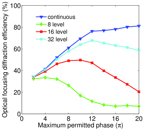
In subsection 3.2, although we have successfully designed the bulk SSBC DOE with high diffraction efficiency, the total thickness of the designed DOE is as large as . In fact, such a thick element is very difficult for photolithographic fabrication of fused silica. In this subsection, the thickness optimization algorithm is adopted to attenuate the thickness. We have calculated the diffraction efficiency of the optimized SSBC DOEs on varying the maximum permitted phase, as shown in Fig. 5. The phase is involved with the average wavelength, which means that 2-phase increase leads to a thickness increment of . The blue curve corresponds to the optimized SSBC DOEs with a continuous phase. From Fig. 5, it is obvious that the diffraction efficiency of the continuous DOE is monotonically increased as the maximum permitted phase is enlarged. It can be understood. With the increase of the maximum permitted phase, because we have more choices in each set of thicknesses, it will be easier to find a thickness that satisfies all the designed wavelengths better.
Considering practical fabrication of the optimized SSBC DOE, the continuous DOE is quantized to have a multilevel profile. The green, red, and cyan curves correspond to the 8-level, 16-level, and 32-level DOEs, respectively. For the designed multilevel DOEs, when the quantization level number is increased, the focusing diffraction efficiency is increased. It is due to the decrease of the quantization error. For a given quantization level number, there exists an optimum maximum permitted phase. It can be explained as follows. When the maximum permitted phase is too small, the selection in each thickness set is strictly limited and thus the optimized thickness deviates very far from the selected thickness for each wavelength. On the other hand, when the maximum permitted phase is too large, it will be much easier to find an accurate thickness . However, for a given quantization level number each step depth is very large, which results in a large boundary quantization error.
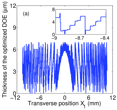
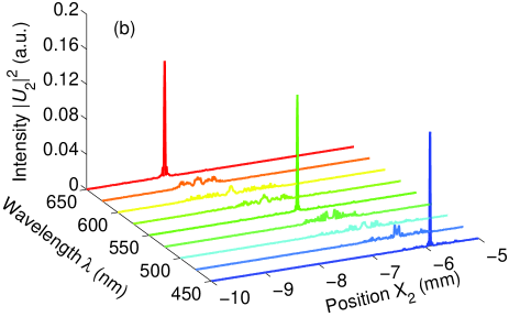
Figure 6(a) shows the boundary profile of the optimized 32-level SSBC DOE, which basically looks like a Fresnel lens. The inset figure magnifies the local part of the DOE boundary. For the optimized 32-level SSBC DOE, numerical results reveal that the optimum maximum permitted phase is 12, corresponding to the maximum thickness of . Under illuminating wavelengths of 0.45, 0.55, and 0.65, the intensity distributions on the output plane is plotted in Fig. 6(b) by the blue, green, and red curves, respectively. It is clearly demonstrated that the optimized 32-level SSBC DOE has good focusing properties for all the three designed wavelengths, as most of the incident power is concentrated in the mainlobe and the side lobes are suppressed well. Numerical results reveal that the average optical focusing diffraction efficiency is for these three wavelengths. The three FWHM sizes are 15.55, 20.73, and 25.91 for incident wavelengths of 0.45, 0.55, and 0.65, respectively. In addition, the transverse preset and real focal positions are the same to be -5.91, -7.23, and -8.54.
Since the sunlight has a continuous spectrum, we are curious about how the optimized 32-level SSBC DOE in Fig. 6(a) performs for other wavelengths? For this reason, we choose six incident wavelengths (475, 500, 525, 575, 600 and 625nm) to calculate the output intensity, as displayed in Fig. 6(b). For these six wavelengths, although the intensity peaks are not high, the energy concentration regions situate in turn with the increase of the incident wavelength. Even if more wavelengths are considered, we can draw a similar conclusion. In solar cell applications, we are more interested in the energy concentration position and efficiency, rather than a higher intensity peak. Numerical results reveal that the corresponding six diffraction efficiencies are 54.61%, 49.03%, 69.16%, 60.03%, 56.08% and 70.40%. Above all, it is concluded that the optimized 32-level DOE not only realizes the expected SSBC functions, but also has a high focusing diffraction efficiency.
4. Conclusions and discussions
In this paper, we propose a new method for designing the single DOE with SSBC functions. The main novelties include these four points. Firstly, we present an analytical thickness formula for the bulk SSBC DOE. Secondly, a thickness optimization algorithm is developed, so that the SSBC DOE can be optimized within an arbitrary thickness range. Thirdly, theoretical simulations demonstrate that the optimized SSBC DOE has a high optical focusing efficiency in the light concentration region. The last but not least, when the thickness of the SSBC DOE is limited in a reasonable scope, it may be fabricated by the modern photolithography technology. More importantly, if a hard mold with a complementary structure is manufactured, mass amount of the SSBC DOEs can be duplicated by using the micro imprint technology. Therefore, it probably provides a cheap way for high-efficiency solar cells.
In this paper, we just select several wavelengths in the visible region instead of the total solar band, because of the following two reasons. One reason is that our main purpose is to demonstrate the validity of the proposed method, and simultaneously the visible range is an important band in the solar spectrum. The other reason is that experimental verifications will be easier to be carried out for the visible light. Fabrications of the optimized SSBC DOE are in progress and their performance will be measured to verify our theoretical predictions.
References
- [1] Razykov T M, Ferekides C S, Morel D, Stefanakos E, Ullal H S and Upadhyaya H M 2011 Solar Energy 85 1580
- [2] Chang L B and Shan K 2011 US patent 0,056,530
- [3] Imenes A G and Mills D R 2004 Sol. Energy Mater. Sol. Cells 84 19
- [4] Kurtz S and Geisz J 2010 Opt. Express 18 A73
- [5] Barnett A, Kirkpatrick D, et al. 2009 Prog. Photovolt: Res. Appl. 17 75
- [6] Tanabe K 2009 Energies 2 504
- [7] Tobias I and Luque A 2002 Prog. Photovolt: Res. Appl. 10 323
- [8] Shockley W and Queisser H J 1961 J. Appl. Phys. 32 510
- [9] Rim S B, Zhao S B, Scully S R, McGehee M D and Peumans P 2007 Appl. Phys. Lett. 91 243501
- [10] Ferry V E, Verschuuren M A, Li H B T, Verhagen E, Walters R J, Schropp R E I, Atwater H A and Polman A 2010 Opt. Express 18 A237
- [11] Raman A, Yu Z F and Fan S H 2011 Opt. Express 19 19015
- [12] Zheng G G, Jiang J L, Xian F L, Qiang H X, Wu H and Li X Y 2011 Chin. Phys. B 20 094201
- [13] Catchpole K R and Polman A 2008 Opt. Express 16 21793
- [14] Atwater H A and Polman A 2010 Nat. Mater. 9 205
- [15] Ren W Z, Zhang G H, Wu Y K, Ding H Y, Shen Q H, Zhang K, Li J W, Pan N and Wang X P 2011 Opt. Express 19 26536
- [16] Hoppe H and Sariciftci N S 2004 J. Mater. Res. 19 1924
- [17] Chutinan A, Kherani N P and Zukotynski S 2009 Optics Express 17 8871
- [18] Park Y, Drouard E, Daif O E, Letartre X, Viktorovitch P, Fave A, Kaminski A, Lemiti M and Seassal C 2009 Opt. Express 17 14312
- [19] Zheng G G, Xian F L and Li X Y 2011 Chin. Phys. Lett. 28 054213
- [20] Rhle S, Greenwald S, Koren E and Zaban A 2008 Opt. Express 16 21801
- [21] Liu Y, Sun S H, Xu J, Zhao L, Sun H C, Li J, Mu W W, Xu L and Chen K J 2011 Opt. Express 19 A1051
- [22] Jonsson G E, Fredriksson H, Sellappan R and Chakarov D 2011 Int. J. Photoenergy 2011 939807
- [23] Xiong B T, Zhou B X, Bai J, Zheng Q, Liu Y B, Cai W M and Cai J 2008 Chin. Phys. B 17 3713
- [24] Kintisch E 2007 Science 317 583
- [25] McCambridge J D, Steiner M A, et al. 2011 Prog. Photovolt: Res. Appl. 19 352
- [26] Bass M, Stryland E W V, Williams D R and Wolfe W L, eds. 1995 Handbook of Optics, Volume II, Devices, Measurements, and Properties 2nd edition (New York: McGraw-Hill Press) p. 33.69
- [27] Goodman J W 1968 Introduction to Fourier Optics (San Francisco: McGraw-Hill Press) Chaps. 3, 4