Demonstration of zero optical backscattering from single nanoparticles
Abstract
We present the first experimental demonstration of zero backscattering from nanoparticles at optical frequencies as originally discussed by Kerker et. al. [M. Kerker, D. Wang, and C. Giles, J. Opt. Soc. A 73, 765 (1983)]. GaAs pillars were fabricated on a fused silica substrate and the spectrum of the backscattered radiation was measured in the wavelength range 600-1000 nm. Suppression of backscattering occurred at 725 nm, agreeing with calculations based on the discrete dipole approximation. Particles with zero backscattering provide new functionality for metamaterials and optical antennas.
pacs:
42.25.Fx, 78.67.Bf, 42.25.HzNanofabrication techniques continue to fuel the search for
structures that exhibit unique optical properties. Among these structures
are optical antennas, which concentrate and
direct light Bharadwaj et al. (2009), and metamaterials that can
mimic optical constants not found in
nature Shalaev (2007); Soukoulis and Wegener (2011). Optical antennas and metamaterials often
capitalize on the plasmonic properties of metal nanostructures Schuller et al. (2010); Kawata et al. (2009). Plasmons,
however, have large non-radiative losses that restrict practical
applications to narrow frequency bands Stockman (2007), even if active gain media are employed Hess et al. (2012). Recently, alternative approaches using dielectric
materials have been proposed for constructing optical
antennas Schuller and Brongersma (2009); Rolly et al. (2012a); Liu et al. (2012); Devilez et al. (2010) and
metamaterials Schuller et al. (2007); Zhao et al. (2009); Jylha et al. (2006).
The optical properties of dielectric nanostructures are strongly influenced by the interaction of electric
and magnetic Mie resonances. Thirty years ago, Kerker et. al.
showed that the
backscattered light from spherical scatterers can be completely suppressed if the
dielectric and magnetic properties of the scatterers are the same () Kerker et al. (1983). A particle with these properties
exhibits equal electric () and magnetic () multipole
coefficients Bohren and Huffmann (1983) that destructively interfere in the backward
propagating direction (first Kerker condition). Until recently, zero backscattering at
visible wavelengths has been a theoretical
curiosity García-Cámara
et al. (2008, 2011, 2010) due to
the lack of magnetic materials () in the optical regime.
Kerker’s condition for zero backscattering can be generalized for spherical particles assuming that the scattered field is sufficiently described by the electric () and magnetic () dipole terms of the Mie expansion Nieto-Vesperinas et al. (2011). In terms of and the electric and magnetic polarizabilities are defined as
| (1) |
respectively, where , with being the refractive index of the surrounding medium and the vacuum wavelength. The two dipoles interfere constructively or destructively depending on their relative phase. In the backward direction the particle’s scattering cross-section is
| (2) |
where is the incoherent sum of the two dipoles, is the phase difference between the dipoles, and , given by
| (3) |
controls the backscattering suppression. A minimum in the backscattered
field will occur whenever the electric and magnetic dipoles are oscillating
in phase (). The minimum will be exactly zero if
is equal to one.

Note that the elimination of the backscattered field in Eq. (2) is
valid even for non-magnetic materials () provided that the dipole approximation
holds. This approximation requires dielectric nanoparticles with a large index of refraction (), such as silicon and germanium Gómez-Medina
et al. (2011); García-Etxarri
et al. (2011).
Recently, the electric and magnetic dipole and
quadrupole resonances have been experimentally measured for silicon
spheres in the visible Kuznetsov et al. (2012); Evlyukhin et al. (2012); Wheeler et al. (2009). The
large refractive index of these nanoparticles make them ideally suited for verifying Kerker’s
theoretical predictions.
In this letter we experimentally demonstrate the
suppression of optical backscattering from dielectric nanoparticles, as
predicted by Kerker Kerker et al. (1983). A recent experiment has demonstrated suppressed backscattering at microwave frequencies Geffrin et al. (2012),
however, a verification at optical wavelengths has not yet been performed. We chose
GaAs as a scattering material due to its large index of refraction
() in the 600 to 1000 nm wavelength
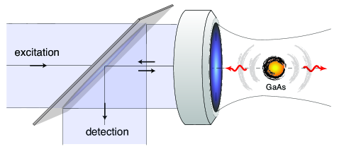
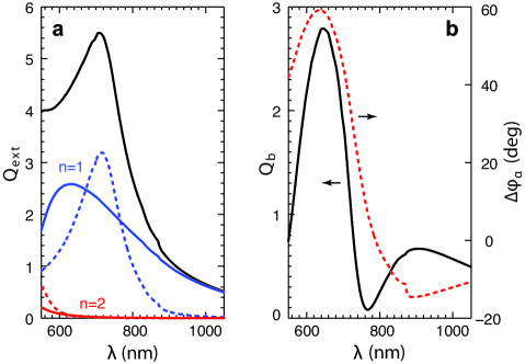
range Palik (1998). The experimental arrangement is sketched in Fig. 1: white light is weakly focused on a sample of well separated GaAs nanoparticles and the backscattered light is separated by a beamsplitter and directed on a spectrometer. Fig. 2(a) is a plot of the extinction
efficiency () for a GaAs sphere of radius =90 nm immersed in a medium of index . The
contributions of the dipole terms (, ) and the quadrupole terms (, )
of are shown as separate curves. The curves show that for wavelengths longer than 600 nm
the electric and magnetic quadrupole terms can be neglected. The backscattering efficiency () is plotted in Fig. 2(b). A minimum in is
located at 775 nm where the relative phase between the electric and
magnetic dipoles crosses zero .

To measure backscattering from GaAs nanoparticles embedded in a uniform
environment we implemented an epitaxial
lift-off technique in conjunction with a water-bonding procedure to attach
a high quality GaAs membrane (grown on a GaAs substrate) to a fused silica
substrate Yablonovitch et al. (1987); Demeester et al. (1993). Direct growth of
GaAs on fused silica is avoided because it results in a high density
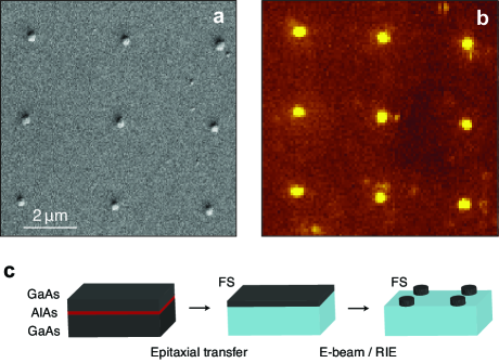
of dislocations. Figure 3(b) illustrates the fabrication steps. Using molecular beam
epitaxy (MBE), a 40 nm sacrificial layer of AlAs was deposited on a GaAs
substrate. On top of the AlAs layer a 1 m film of GaAs was
grown. Using the epitaxial lift-off procedure, the 1 GaAs film was
transfered to a fused silica substrate. The transfered GaAs film was
initially reduced to a thickness of 150 nm by reactive ion etching
(RIE). An array of 175 nm diameter discs was then patterned in a
Poly(methyl methacrylate) (PMMA) resist using e-beam
lithography. After developing the resist, GaAs pillars were created by
RIE. The leftover PMMA was removed with an additional oxygen plasma
etch. Fig. 3(a) shows a scanning electron microscope (SEM)
image of the fabricated structures. To verify that no residual GaAs
remained after etching, a confocal scanning image of the photoluminescence
was taken with an excitation laser of nm. The confocal image
in Fig. 3(b) shows strong signal from the GaAs pillars with
limited luminescence from the fused silica substrate.

Backscattering measurements were done using a standard inverted microscope with
a fiber-coupled tungsten halogen white light source (c.f Fig. 1). To create a uniform
environment, and eliminate any back-reflections, index matching oil covered
the top of the sample. The sample was broadly illuminated by weakly
focusing the white light source through an oil immersion objective. The
backscattered light was collected with the same objective and sent to
either an avalanche photodiode (APD) or a spectrometer. A 10 nm bandpass
filter was placed in front of the APD and the sample was scanned by a
piezo positioning stage to form an image. Spectra of single GaAs
pillars were acquired in the wavelength range of 600-1000 nm. The
collection volume was limited either by the APD detector area or the spectrometer
silt width. This ensured that light from only a single scatterer was detected even though the
sample was broadly illuminated.
The recorded spectra and APD images were corrected for source spectrum non-uniformity, transmission losses, and detector efficiencies. A baseline spectrum [] was recorded by replacing the sample with a mirror. Additionally, the background spectrum [] measured on the fused silica substrate away from the GaAs pillars was subtracted. This background resulted from a slight refractive index mismatch between substrate and index-matching oil. The final backscattering efficiency is calculated as
| (4) |
where is the recorded spectrum. The pre-factor is a calibration scaling factor.

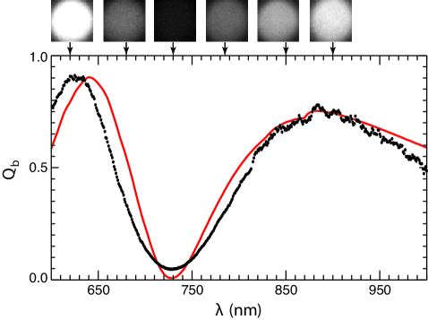
Figure 4 shows the resulting backscattering efficiency recorded for a
single GaAs pillar. The spectrum has a pronounced dip at
725 nm where the backscattered field is suppressed due to the
interference between the electric and magnetic dipole components. Though
the suppressed backscattered field is obvious, there are two notable
differences in the spectral shape when comparing to the Mie theory of
Fig. 2. First, the scattering amplitude below 700 nm is
suppressed and, second, the location of the minimum is blue shifted. Both
of the differences are attributed to the fact that the structure is a
pillar rather than a sphere. Compared to a sphere of the same volume, a
pillar with an aspect ratio (height/diameter) below one will have the
location of the minimum blue shifted and the scattering peak to the left of
the minimum suppressed (See Supplementary Material sup ). The
solid curve in Fig. 4 is a simulation of the backscattered
field of a GaAs pillar calculated using the discrete dipole approximation
Draine and Flatau (1994). The simulated structure has a height of 137 nm and a
diameter of 165 nm, which is within 10% of the initial design
parameters. The sequence of images above Fig. 4 are backscattering images with bandwidth of 10 nm and center wavelengths
indicated by the arrows. At the
location of the spectral minimum the image of the scatterer fades into the
background.
In conclusion, we have shown the first experimental verification of
Kerker’s theoretical prediction of zero backscattering in the optical
wavelength range. Using pillars, rather than spheres, slight shifts of the
wavelength of minimum backscattering can be observed. This shift as well as the reshaping of the spectrum
are reproduced with calculations based on the discrete dipole approximation. Understanding
and verifying the response of single dielectric nanoparticles is crucial in
any bottom-up nanofabrication technique. The remarkable properties of these particles, with zero backscattering but significant light dispersion in forward direction, suggest intriguing technological applications, for example as light diffusing elements in solar cells. Using similar GaAs structures,
experiments involving arrays of scatterers Evlyukhin et al. (2010) or dielectric
antennas manipulating magnetic dipoles Schmidt et al. (2012); Rolly et al. (2012b) are
possible.
Acknowledgements.
This work was funded by the U.S. Department of Energy (Grant No. DE-FG02-01ER15204).References
- Bharadwaj et al. (2009) P. Bharadwaj, B. Deutsch, and L. Novotny, Adv. Opt. Phot. 1, 438 (2009).
- Shalaev (2007) V. M. Shalaev, Nature Photon. 1, 41 (2007).
- Soukoulis and Wegener (2011) C. M. Soukoulis and M. Wegener, Nature Photon. 5, 523 (2011).
- Schuller et al. (2010) J. A. Schuller, E. Barnard, W. Cai, Y. C. Jun, J. White, and M. L. Brongersma, Nature Mat. 9, 193 (2010).
- Kawata et al. (2009) S. Kawata, Y. Inouye, and P. Verma, Nature Photon. 3, 388 (2009).
- Stockman (2007) M. Stockman, Phys. Rev. Lett. 98, 177404 (2007).
- Hess et al. (2012) O. Hess, J. B. Pendry, S. A. Maier, R. F. Oulton, J. M. Hamm, and K. L. Tsakmakidis, Nature Mat. 11, 573 (2012).
- Schuller and Brongersma (2009) J. A. Schuller and M. L. Brongersma, Opt. Express 17, 24084 (2009).
- Rolly et al. (2012a) B. Rolly, B. Stout, and N. Bonod, Opt. Express 20, 20376 (2012a).
- Liu et al. (2012) W. Liu, A. E. Miroshnichenko, D. N. Neshev, and Y. S. Kivshar, ACS Nano 6, 5489 (2012).
- Devilez et al. (2010) A. Devilez, B. Stout, and N. Bonod, ACS Nano 4, 3390 (2010).
- Schuller et al. (2007) J. A. Schuller, R. Zia, T. Taubner, and M. L. Brongersma, Phys. Rev. Lett. 99, 107401 (2007).
- Zhao et al. (2009) Q. Zhao, J. Zhou, F. Zhang, and D. Lippens, Mater. Today 12, 60 (2009).
- Jylha et al. (2006) L. Jylha, I. Kolmakov, S. Maslovski, and S. Tretyakov, J. Appl. Phys. 99, 043102 (2006).
- Kerker et al. (1983) M. Kerker, D. Wang, and C. Giles, J. Opt. Soc. Am. 73, 765 (1983).
- Bohren and Huffmann (1983) C. F. Bohren and D. R. Huffmann, Absorption and Scattering of Light by Small Particles (Wiley, New York, 1983).
- García-Cámara et al. (2008) B. García-Cámara, F. Moreno, F. González, J. M. Saiz, and G. Videen, J. Opt. Soc. Am. A 25, 327 (2008).
- García-Cámara et al. (2011) B. García-Cámara, R. Alcaraz de la Osa, J. M. Saiz, F. González, and F. Moreno, Opt. Lett. 36, 728 (2011).
- García-Cámara et al. (2010) B. García-Cámara, J. María Saiz, F. González, and F. Moreno, Optics Comm. 283, 490 (2010).
- Nieto-Vesperinas et al. (2011) M. Nieto-Vesperinas, R. Gómez-Medina, and J. J. Sáenz, J. Opt. Soc. Am. A 28, 54 (2011).
- Gómez-Medina et al. (2011) R. Gómez-Medina, B. García-Cámara, I. Suárez-Lacalle, F. González, F. Moreno, M. Nieto-Vesperinas, and J. J. Sáenz, J. Nanophotonics 5, 053512 (2011).
- García-Etxarri et al. (2011) A. García-Etxarri, R. Gómez-Medina, L. S. Froufe-Pérez, C. López, L. Chantada, F. Scheffold, J. Aizpurua, M. Nieto-Vesperinas, and J. J. Sáenz, Opt. Express 19, 4815 (2011).
- Kuznetsov et al. (2012) A. I. Kuznetsov, A. E. Miroshnichenko, Y. H. Fu, J. Zhang, and B. Luk’yanchuk, Sci. Rep. 2, 492 (2012).
- Evlyukhin et al. (2012) A. B. Evlyukhin, S. M. Novikov, U. Zywietz, R. L. Eriksen, C. Reinhardt, S. I. Bozhevolnyi, and B. N. Chichkov, Nano Lett. 12, 3749 (2012).
- Wheeler et al. (2009) M. S. Wheeler, J. S. Aitchison, J. I. L. Chen, G. A. Ozin, and M. Mojahedi, Phys. Rev. B 79, 073103 (2009).
- Geffrin et al. (2012) J. Geffrin, B. García-Cámara, R. Gómez-Medina, P. Albella, L. Froufe-Pérez, C. Eyraud, A. Litman, R. Vaillon, F. González, M. Nieto-Vesperinas, et al., Nature Commun. 3, 1171 (2012).
- Palik (1998) E. D. Palik, Handbook of Optical Constants of Solids (Elsevier, San Diego, 1998).
- Yablonovitch et al. (1987) E. Yablonovitch, T. Gmitter, J. Harbison, and R. Bhat, Appl. Phys. Lett. 51, 2222 (1987).
- Demeester et al. (1993) P. Demeester, I. Pollentier, P. Dedobbelaere, C. Brys, and P. Vandaele, Semicond. Sci. Technol. 8, 1124 (1993).
- (30) See supplemental material at [url will be inserted by publisher] for scattering properties of gaas cylinders.
- Draine and Flatau (1994) B. T. Draine and P. J. Flatau, J. Opt. Soc. Am. A 11, 1491 (1994).
- Evlyukhin et al. (2010) A. B. Evlyukhin, C. Reinhardt, A. Seidel, B. S. Luk’yanchuk, and B. N. Chichkov, Phys. Rev. B 82, 045404 (2010).
- Schmidt et al. (2012) M. K. Schmidt, R. Esteban, J. J. Sáenz, I. Suárez-Lacalle, S. Mackowski, and J. Aizpurua, Opt. Express 20, 13636 (2012).
- Rolly et al. (2012b) B. Rolly, B. Bebey, S. Bidault, B. Stout, and N. Bonod, Phys. Rev. B 85, 245432 (2012b).