A unified model of droplet epitaxy for compound semiconductor nanostructures: experiments and theory
Abstract
We present a unified model of compound semiconductor growth based on kinetic Monte Carlo simulations in tandem with experimental results that can describe and predict the mechanisms for the formation of various types of nanostructures observed during droplet epitaxy. The crucial features of the model include the explicit and independent representation of atoms with different species and the ability to treat solid and liquid phases independently. Using this model, we examine nanostructural evolution in droplet epitaxy. The model faithfully captures several of the experimentally observed structures, including compact islands and nanorings. Moreover, simulations show the presence of Ga/GaAs core-shell structures that we validate experimentally. A fully analytical model of droplet epitaxy that explains the relationship between growth conditions and the resulting nanostructures is presented, yielding key insight into the mechanisms of droplet epitaxy.
I Introduction
Nanotechnology involves the manipulation of matter at the nanoscale in order to take advantage of the physical properties of materials which arise by a fine tuning of shape and size. Due to quantum confinement effects, three dimensional semiconductor nanostructures can behave as artificial atoms and, like natural atoms, show a discrete spectrum of energy levels Kastner (1993). In contrast to actual atoms, the electronic properties of quantum nanostructures can be finely tuned by adjusting structural parameters such as size, composition and morphology. The latter parameter is the most relevant for the control of quantum nanostructure electronic properties, as tiny variations in morphology or composition can cause dramatic changes on the band structure Li and Wang (2003).
One of the most common methods for the fabrication of quantum nanostructures is the growth of lattice-mismatched III-V semiconductor materials via the Stranski-Krastanov (SK) mode. SK growth exploits the self-assembly of pyramidal-like quantum dots (QDs), driven by the relaxation of lattice mismatched strain accumulated in the epilayer. Despite the high success of the technique, which led to fundamental physical understanding and a variety of applications, the available design degrees of freedom remain limited. The precise engineering of size and shape of QDs via SK self-assembly remains problematic, thus limiting the possibilities for the design of arbitrary electronic and optical properties.
To overcome the SK growth limitations, a fully kinetic limited growth procedure called droplet epitaxy (DE) was introduced Koguchi et al. (1991, 1993). Unlike SK self-assembly, DE does not rely on strain for the formation of three dimensional nanostructures. Instead, DE is based on the sequential deposition of III and V column elements at controlled temperatures and fluxes and, as such, is a bottom-up fabrication and patterning technique. An initial deposition of metallic group III such as Ga in a group V free environment leads to the formation of nanometer size liquid droplets. Subsequent exposure of the liquid droplets to the group V vapor causes them to crystallize into quantum dots, by which we mean compact, three-dimensional nanostructure Koguchi and Ishige (1993); Watanabe et al. (2000). A variety of nanostructures may be obtained using this technique, ranging from compact quantum dots, quantum rings, and core shell structures Watanabe et al. (2000); Mano et al. (2005); Somaschini et al. (2009, 2012); Somaschini et al. (2010a, 2011a). While experimental observations evoke likely mechanisms, a unified model for the formation of various nanostructural morphologies via DE is still needed. Understanding the precise mechanisms behind their formation is critical to controlling the various properties such as shape, size, and composition, which in turn affect the macroscopic behavior of devices based on such quantum nanostructures.
Kinetic Monte Carlo (KMC) simulation is a useful tool for developing and testing models of epitaxial growth and have shed light on the important processes for a wide range of scenarios. Previous KMC simulations of GaAs systems modeled homoepitaxial growth on a cubic lattice. Among the earliest simulations, a single component was used to model epitaxial growth, varying energy parameters to account for the expected effect on diffusivity by different Ga/As deposition ratios Shitara et al. (1992). Two-component simulations have also been performed Kawamura and Ishii (1999, 2001); Ishii and Kawamura (1999) to study aspects of film growth such as the transition from two dimensional island formation to step-flow growth. Such simulations, however, are necessarily over small areas and are valid only for a limited range growth parameters. In most cases these simulations are unable to model growth regimes in which the group V to group III ratio in the growing film is not unity, as in the case in droplet epitaxy.
The simulations presented in this paper are designed to capture a wide range of phenomenology in epitaxial growth, with an emphasis on the growth from the liquid phase. We chose to examine droplet epitaxy first, but the simulation and analytical methodologies presented here are applicable to other growth mechanisms, specifically nanowire grown by the Vapor-Liquid-Solid (VLS) method. In both VLS and DE growth, a liquid metal reacts with vapor, resulting in crystallization at the liquid-solid interface. In DE, the metal is consumed during this crystallization process. In VLS, the metal is either not consumed or consumed more slowly than in DE, resulting in structures of length scale larger than the original liquid droplet.
In this paper, we present experimental and simulation results that shed light on the exact mechanisms behind the formation of nanostructures in droplet epitaxy. We introduce a KMC model (Section II) that is capable of simulating the formation of nanostructures at all stages, from homoepitaxial growth, to liquid metal droplet formation and subsequent crystallization. The model represents Ga and As atoms explicitly, and treats liquid and solid phases independently. Although atomistic, the simulations form large-scale global structure consistent with experimental results in a reasonable amount of time. As an initial validation of the model, GaAs homoepitaxy simulations are compared with analogous experiments, accurately reproducing a surface termination phase diagram (Section III). We then turn our attention to the main thrust of the paper, the nanostructural dependence on growth conditions during droplet epitaxy. We present experimental results exhibiting this dependence, along with corresponding simulations (Section IV). The model can capture the broad range of nanostructures observed in the experiments with the correct qualitative dependence on growth parameters. Moreover, simulations predict the presence of Ga/GaAs core-shell structures, which are difficult to observe unambiguously in experiments. The existence of both monocrystalline and polycrystalline shells suggest two independent mechanisms of their formation: a morphological instability of the crystallization front or nucleation at the vapor-liquid interface. We show by simulation that nucleation-induced shell structures may be recrystallized into fully crystallized GaAs islands by annealing in high temperature (Section IV.2.1). In the case of the instability-driven shell formation, we provide simulation and experimental evidence to suggest the presence of a Mullins-Sekerka instability (Section IV.2.2). Lastly, we develop a fully analytical model (Section V) that describes the existence of the structures observed and their dependence on growth conditions. The theoretical model agrees well with simulation and experimental results.
II Kinetic Monte Carlo model
Prior work in simulating GaAs systems focused on homoepitaxial growth and studied associated phenomena such as step density Shitara et al. (1992) and growth modes of GaAs filmsKawamura and Ishii (1999). In these simulations, surface diffusion of adatoms played the central role, and because of the stoichiometric nature of epitaxial growth, a simple cubic lattice and the solid-on-solid constraint sufficed in modeling key aspects of this process. Droplet epitaxy however, poses several issues that cannot be captured by earlier models. During DE, the system is inherently non-stoichiometric in that the relative concentrations of Ga and As atoms on the surface are different from one another and so care must be taken to model liquid droplet formation. Processes other than surface diffusion, such as events within liquid and at the liquid-solid interface, play a key role and cannot be captured by a simple solid-on-solid model. Lastly, DE results in large-scale nanostructures on the order of 10s to 100s of nm so that the simulations must be performed efficiently within large domains.
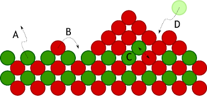
We simulate the homoepitaxial growth and droplet epitaxy experiments with a KMC model that attempts to address the relevant processes in DE. In the model, atoms occupy positions on a 1+1 dimensional analog of the zinc blende lattice illustrated in Figure 1. Each position on the lattice is adjacent to four nearest neighbors and four next-nearest neighbors. Lattice sites are vacant or occupied by either a Ga or As atom. The 1+1 dimensional approach naturally hinders our model to catch effects that are associated to the three-dimensional crystal structure and to atomic rearrangements driven by non-local energetics like surface reconstruction phase changes. Specifically surface reconstruction dynamics leads to changes in adatom surface mobility, both in terms of diffusion length and diffusivity anisotropy, and in adatom incorporation into the crystal structure. These effects are at the origin, in DE, of the observed dependence on substrate temperature and preparation procedure in the droplet formation critical coverage during the initial Ga deposition and of the shape and anisotropy of control of the quantum nanostructures that are possible thanks to fine control of surface reconstruction dynamics Somaschini et al. (2010b, c). The simplicity of the model implies such effects cannot be captured, in line with previous work on KMC modeling. We note here that other theoretical models can capture surface reconstructions Chakrabarti et al. (2006). The processes that are captured and studied in this paper, however, yield first-order insight to the growth mechanisms in DE.
In each Monte Carlo step, one of four local events alters at most two positions on the lattice. Atoms may desorb from the surface (A in Figure 1), diffuse on the surface (B), exchange with neighboring atoms (C), or adsorb onto a vacant position on the surface (D). The model does not enforce a solid-on-solid constraint. Instead, atom configurations are required to be connected, i.e. there must exist a chain of atoms (through nearest neighbor bonds) between any two atoms in the configuration. While connectedness is inherently a global property, the requirement is approximated by enforcing the property on all local neighborhoods. Any event resulting in a disconnected configuration is disallowed.
Event rates are determined by simple nearest and next-nearest neighbor bond-counting. Due to the multi-species nature of the model, several bonding energies must be specified. Specifically, nearest and next-nearest neighbors are bonded by energies that depend solely on the species of the two connected atoms. Nearest neighbor bonding energies are given by three parameters and . Next-nearest neighbor bonds are only assigned between atoms of the same species and are denoted and . In this way, Ga and As only interact through nearest-neighbor bonds, whereas Ga-Ga and As-As interact through nearest and next-nearest neighbor bonds. The parameter values used in the simulations are summarized in Table 1. These energy values imply that the Ga-As bonds are energetically preferred, while weak As-As bonds effectively eliminate excess As by desorption. The bonding energies were calibrated from the homoepitaxy (Section III) and liquid droplet simulations (Section IV) to match qualitative experimental assumptions and observations. Within the homoepitaxy simulations, the Ga-As bond strengths were tuned in order to observe a transition from rough island formation in the low temperature regime to a smooth step-flow growth mechanism in high temperatures Orme et al. (1994). In the case of liquid droplet simulations, we tune the Ga-Ga bond strength to match liquid droplet statistics such as droplet width and number density.
|
|
Monte Carlo transition rates from atom configuration to configuration are taken to be of an Arrhenius form:
where is a constant rate prefactor, is temperature, and is the activation energy for a particular event.
For surface diffusion, is simply the sum of the bonding energies about the diffusing atom. For the desorption of an As atom, the activation energy is the sum of the bonding energies about the desorbing atom and an additional desorption barrier eV, its value calibrated by homoepitaxial simulations described in Section III. The desorption of Ga is disallowed. In the case of atom-atom exchanges, which occur within a liquid droplet, we use a base energy barrier for the As diffusion barrier in liquid Ga, described in more detail below. To facilitate exchanges occurring at the liquid-solid interface, for which we must take solid bonds into account, we define an intermediate state in which the exchanging atoms are replaced by an intermediate species H. Bonding energies between Ga or As atoms and H atoms are obtained by averaging over and , e.g.
The activation energy of an atom-atom exchange at the liquid-solid interface is then taken to be the sum of the base barrier and the change in bonding energies between the original and the intermediate states.
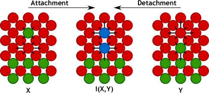
For example, we consider the attachment and detachment of an As atom onto the liquid-solid interface, as illustrated in Figure 2. We denote the states before and after the detachment as , respectively, and the intermediate state as defined above by . The change in energy between states and , describing the additional barrier for attachment can be computed from a small number of relevant bonds, indicated by black lines in the figure. The total activation energy for attachment is then given by
We may calculate the activation energy for detachment in a similar manner:
The forms of the attachment and detachment barriers and indicate what physically occurs during the transitions, namely the formation/removal of one next-nearest neighbor Ga-Ga bond and one next-nearest neighbor As-As bond.
II.1 Liquid Barriers
Because we wish to simulate liquid droplet epitaxy, our model identifies liquid neighborhoods in which events are assigned different energy barriers to account for the salient physics within a liquid droplet. The diffusion of As through a liquid droplet occurs atomistically as an exchange event between the diffusing As atom and a Ga atom neighbor. Such an atom-atom exchange event is deemed a liquid event if there is at most one As atom total within the neighborhood of the exchanging atoms.
Further, such exchanges in the liquid are categorized as occurring on either the surface or bulk of a droplet. A surface liquid exchange event is one in where there is at least one vacancy within the neighborhoods of the exchanging atoms. These events represent the incorporation of an As atom from the surface into the bulk of the droplet or vice versa and are given a constant activation energy barrier eV. The particular value of is slightly larger than the 1 eV barrier for the diffusion of an As adatom on the surface of a liquid droplet. A liquid event that does not occur on the surface is categorized as a liquid bulk event and is assigned the energy barrier , which represents the diffusion barrier of an As atom within the bulk of the liquid. The value eV was calibrated by the droplet epitaxy simulations described in Section IV. Only after this model was completed did we become aware of the experimental work of Gorokhov et al. Gorokhov et al. (1984) who reported the energy barrier for diffusion As in Ga of approximately 0.7 eV.
Because of its ability to handle the liquid phase independently, along with its multi-component nature, the model may be minimally adapted to simulate other growth modes in which liquid droplets are used. In particular, the model has been applied to simulate nanowire growth by the VLS method Reyes (2013). Here, identifying liquid neighborhoods is important to prescribe special energy barriers for the conversion of vapor phase to a solid one, mimicking the catalytic effect of the liquid droplet. Additionally, without the SOS constraint, the model captures phenomena such as nanowire bending.
II.2 Detailed Balance
In order to discuss detailed balance, we consider the behavior of our model in the absence of deposition and desorption Biehl (2005). Under such conditions, we assume the incorporation of an As atom from the surface of a droplet into the liquid bulk to be a rare event. The rates of the remaining events (i.e. surface diffusion and atom-atom exchanges both within the liquid and at the liquid-solid interface) satisfy detailed balance with respect to the Boltzmann distribution
where is the energy of the state obtained by bond counting, using bonding energies in Table 1. For these events , the activation energies are of the form
| (1) |
where is a transition state between and and is an additional barrier. Detailed balance follows since we have required that and be symmetric with respect to their arguments.
For surface diffusion, is the state with the diffusing atom removed and . Because the reverse event is also a surface diffusion event, it follows that and . For atom-atom exchanges, is the state where the exchanging atoms are replaced with intermediate species H, and hence , and . Note that it was claimed above that for an As atom diffusing through liquid Ga, an activation barrier was used without any further contribution to the barrier from bond counting. This is consistent with the generalized description of the activation energy in equation (1), because in this case , i.e. no bonds are formed/removed during the diffusion of As in liquid Ga.
II.3 Implementation
Because of the time and length scales associated to the nanostructures we wish to simulate, an efficient implementation of the KMC algorithm is important. A rejection-free sampling of rates is achieved by the standard binary-tree data structure containing partial sums of the ratesBlue et al. (1995), achieving sampling by binary search and tree updates, where is the number of atoms. As the algorithm proceeds, event rates for several atoms must be recomputed at every step. A rate caching technique is employed to remove repeated rate calculations by taking advantage of the recurrent nature of local neighborhoods within KMC Reyes (2013). This procedure leads to significant performance gains.
III Homoepitaxy
As an initial application and validation of the simulations, we model GaAs substrate growth at various growth conditions. It is known that the surface reconstruction of a GaAs substrate depends on both the temperature and the relative deposition rates of Ga and As Ohtake (2008). In 1+1 dimensions, simulations cannot reproduce surface reconstructions. Instead, we measured surface termination and its dependence on temperature and incoming deposition rates. The simulation results were then compared to experimental data.
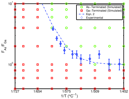
Experiments on GaAs(001) were carried out using molecular beam epitaxy (MBE) equipped with a solid source for Ga and a valved source for As4. Substrates were initially heated under As4 overpressure to desorb the native oxide layer. A 75 nm GaAs buffer layer was then grown at a substrate temperature of with a Ga deposition rate of 0.4 monolayers per second (ML/s) and an As4 growth rate of at least 2 ML/s, as measured by reflection high energy electron diffraction (RHEED) oscillations Ferguson et al. (1992). After growing the GaAs buffer, the substrate temperature was fixed between and . GaAs was then grown with a Ga rate of 0.6 ML/s while the As rate was slowly reduced from 3.9 ML/s to 1.0 ML/s. During the growth, the RHEED pattern was monitored for the change from an As-terminated reconstruction to a Ga-terminated reconstruction. Consistent with the expected result, at high substrate temperatures the As rate required to maintain an As-terminated surface increases with temperature. At lower temperatures, the necessary As rate becomes invariant with temperature.
To simulate GaAs substrate growth, both Ga and As were deposited simultaneously on initially flat, As-terminated substrate. The Ga deposition rate was fixed at 0.37 ML/s, while the As deposition rate was varied so that the deposition ratio ranged between .5 and 10. Rates (reported in ML/s) here and throughout this paper describe the rate at which atoms are added to the system. The observed stoichiometric growth of the film is an emergent property of the model rather than explicitly enforced through deposition rates. This is manifest in the stoichiometry observed over a broad range of deposition ratios.
The temperature was varied between and . Five monolayers of total material was deposited, and surface Ga concentration was measured at regular intervals during the deposition of the last two monolayers. Figure 3 is a surface termination phase diagram as a function of deposition rate and temperature for both experimental and simulation results. Red squares indicate the conditions where simulations show a predominantly Ga-terminated surface, while green circles are conditions yielding a predominantly As-terminated surface. Experimentally determined transition from the As-terminated to the Ga-terminated reconstructions as determined by RHEED are shown as blue diamonds and indicate a good agreement between simulation and experimental data.
The relevant parameter that controls surface termination is the As desorption barrier . Varying this parameter effectively shifts the above phase diagram horizontally. The value eV is fitted to experiments. This value, combined with the energy values in Table 1 yield a total activation energy of
for the desorption of an As adatom from a Ga terminated substrate, comparing favorably to experimental resultsLiang and Tu (1993); Yamaguchi and Horikoshi (1992). Moreover, the specific parameter value does not significantly impact the qualitative shape of the phase diagram. That is, independent of , the simulations capture a constant critical deposition ratio in the low temperature regime and its transition to an increasing critical ratio as temperature increases.
Due to the simplicity of the model, individual As atoms are deposited on the surface rather than As4 molecules. In this homoepitaxy study, the adsorption/desorption processes, and in particular, the value of was tuned to match the macroscopic properties surface termination and concentration. As such, the fitted value of serves as an accurate measure of As growth and incorporation onto the substrate. Other surface As kinetic effects, including those determined by surface reconstruction dynamics on the local scale, may not be captured by the model. However, in the DE growth procedure, these effects appear to be relevant mostly in determining the extended nanostructure shape control peculiar to DE Somaschini et al. (2010b) or in the extremely low temperature and high As fluxes. We therefore believe that such effects should lead to minor modifications in the description of the DE processes that are studied in this paper.
An analytical expression for the boundary between Ga-terminated and As-terminated substrates can be determined. During homoepitaxial growth, several processes occur, including surface diffusion and As desorption, but to first order we may approximate the system in a quasi-static deposition/ desorption-limited regime. In this regime, the transition between the As and Ga-terminated surface occurs when the amount of Ga on the impinging upon the surface (given by ) is equal to the net rate of As growth (given by ), where is the desorption rate of , taken as the harmonic average of the desorption rates for an As adatom on a Ga-terminated surface (with desorption energy barrier 2.2 eV) and a As atom on a Ga-terminated surface with one nearest or next nearest neighbor (with desorption barrier 2.3 eV). This boundary is given by the equation
| (2) |
and agrees well with both simulation and experiments.
IV Liquid Droplet Epitaxy
The main thrust of this work was to accurately capture the processes relevant to liquid droplet formation and crystallization. The experiment and simulations proceed in two main steps, which are at the basis of the droplet fabrication of GaAs/AlGaAs quantum nanostructures Watanabe et al. (2000). First, Ga is deposited onto the substrate by MBE, forming liquid Ga droplets. Next the droplets are crystallized by the introduction of an As flux. Depending on growth conditions such as temperature and As overpressure, the actual morphology upon crystallization can vary Watanabe et al. (2000). The observed nanostructures may range from fully crystallized compact quantum dots, to nanorings and even etched holes Wang et al. (2007); Somaschini et al. (2009); Somaschini et al. (2010b); Mano et al. (2005); Kuroda et al. (2005).
IV.1 Quantum Dots and Nanorings
IV.1.1 Experimental methodology
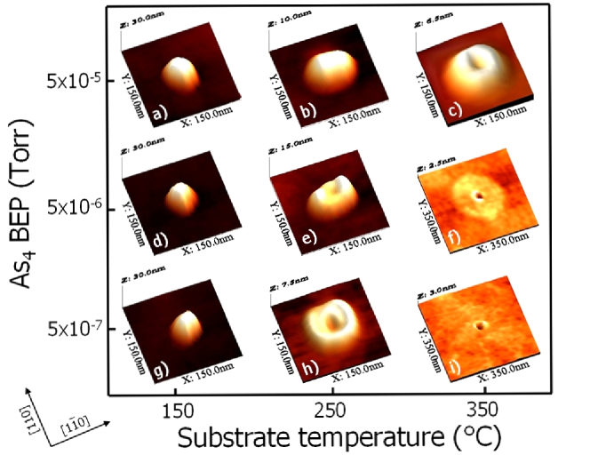
In order to experimentally assess the exact dependence of droplet epitaxy nanostructures on the growth condition, we prepared a matrix of samples, sampling the typical droplet epitaxy ranges for substrate temperatures and As4 beam equivalent pressure (BEP). The samples were prepared following the standard procedure for droplet epitaxy Watanabe et al. (2000, 2001); Kuroda et al. (2002). After the oxide removal and the GaAs buffer layer growth ( on thick at ) to ensure the atomic smoothness of the surface, a 200 nm thick Al0.3Ga0.7As barrier layer is grown at the same temperature of . The presence of an AlGaAs barrier permits the use of the fabricated structures, once capped with another AlGaAs layer, as morphology controlled quantum nanostructures. We do not expect the Al content of the barrier to influence the obtained GaAs nanostructure morphology as the AlGaAs barrier is buried under a 1.75 ML GaAs top layer which forms on the surface during the following Ga deposition step Watanabe et al. (2000); Sanguinetti et al. (2002).
Prior to the deposition of Ga, the As cell is closed and the background pressure reduced below Torr. Ga droplets are then formed on the substrate surface by supplying 2.5 ML of Ga at with a deposition rate of 0.08 ML/s. Many nearly hemispherical Ga droplets form at a density of cm-2. The average droplet diameter and height are 50 nm and 20 nm, respectively. The same Ga droplet preparation procedure is used for each sample in order to assure the same droplet density before the crystallization procedure. We then explored the nanostructure fabrication parameter space by varying the substrate temperature and the As4 BEP used for the crystallization of Ga droplets. Nine different samples are prepared by systematically varying the temperature between 150 and and the As4 BEP between and Torr. The crystallization time is kept constant (10 min.) to ensure the complete reaction of the Ga contained in the droplets with As atoms. The morphological dependence of the fabricated nanostructures, measured by Atomic Force Microscopy (AFM) on temperature and As overpressure is summarized in Figure 4. From this data, it is clear that compact islands form at low temperature, and as the As overpressure is reduced or the temperature is increased, the nanostructures become rings. At the highest temperature and lowest As overpressure, only holes remain in the place of the droplet. From large area scans (not shown here) the number of GaAs nanostructures per unit area are in excellent agreement with the original droplets density. Each droplet was thus transformed into a GaAs nanostructure at the end of the crystallization procedure.
IV.1.2 Simulations
The simulations were performed in a similar manner to the experiments outlined above. However, in order to simplify the analysis, the temperature was maintained constant throughout each simulation. This is justified by the observation that the Ga deposition temperature affects droplet density but does not play a relevant role in determining droplet crystallization dynamics. Simulations proceed as follows:
-
1.
Ga atoms are deposited on a flat, As-terminated GaAs substrate at a rate of 0.1 ML/s at temperature until 4.0 monolayers are deposited;
-
2.
The system is then annealed for 60 seconds in the absence of deposition;
-
3.
After annealing, an As flux is introduced by the deposition of As at a rate of ML/s until the system attains equilibrium.
The growth parameters and were varied in order to study their effect on the resulting morphology. The temperature ranged between and , while the As deposition rate ranged between 0.1 ML/s and 4 ML/s Within this range of growth parameters, we are able to simulate the formation of a variety of nanostructures similar to those observed experimentally.
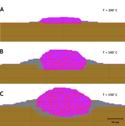
During the first phase of the simulation, Ga atoms are deposited on a flat, initially As-terminated GaAs substrate. The first monolayer of Ga deposited is consumed in creating a layer of Ga, resulting in a Ga terminated substrate. Afterwards, the remaining Ga atoms diffuse along the surface and eventually nucleate hemispherical droplets as the system attempts to minimize the vapor-liquid interface. During droplet formation, simulations show that liquid Ga etches into GaAs, and the amount of etching is regulated by temperature, as illustrated in Figure 5. Higher temperatures result in more significant etching. This is in agreement with experimental observations Heyn et al. (2011); Wang et al. (2007). As the droplet etches into the substrate liquid Ga atoms displace substrate As atoms, which subsequently attach near the triple junction. In addition, some of the displaced substrate material is wicked out of the droplet in a step-flow growth mode. The relevant model parameter controlling the effect of etching is the additional barrier for atom-atom exchanges, . The value eV was selected to fit qualitative experimental observations on the amount of etching occurring at various temperatures.
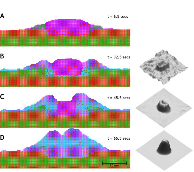
Once the liquid droplet has formed and come to equilibrium, an As flux is introduced to initiate crystallization. Arsenic atoms deposited near or on the droplet diffuse through the liquid quickly Gorokhov et al. (1984) and attach most typically near the triple-junction. Such crystallization results in a growing GaAs front and the droplet is crystallized inward. If no nucleation occurs at the vapor-liquid interface and the GaAs fronts coalesce, a fully crystallized quantum dot forms in place of the liquid droplet. Such is the case for moderate temperatures and deposition rate.
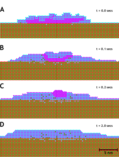
Figure 6 is a sequence of simulation snapshots illustrating the crystallization of a liquid droplet resulting in a quantum dot (left panel), along with analogous AFM images of the GaAs fronts obtained experimentally (right panel). The simulation images in the figure illustrate a typical quantum dot grown at and ML/s. The general trend is that a Ga drop forms once enough Ga has been deposited on the surface (Figure 6A), followed by crystallization near the vapor/liquid/solid triple junction upon exposure to As flux (B,C). As crystallization progresses, the liquid Ga is consumed, resulting in a fully crystallized quantum dot (D). Experimental images (Figure 6, right panel) were obtained from individual samples prepared according to the experimental procedure outlined above, varying As exposure time. The unreacted liquid Ga was removed from the samples before imaging by selective wet etching Somaschini et al. (2009), thus showing GaAs fronts at various stages during crystallization. The AFM images confirm the growth mechanism observed in the simulations during crystallization.
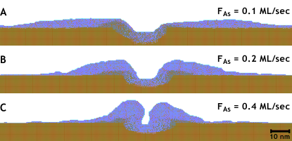
Besides compact quantum dots, other nanostructures are predicted by the simulation by considering a broad range of temperatures and As fluxes. For example, if is sufficiently low or is sufficiently large, the simulations show the formation of nanorings upon crystallization. The exact morphology of the nanorings is sensitive to the growth conditions. Figure 7 shows the morphological dependence of the rings on , fixing . At low As deposition rate ( ML/s), broad and short nanorings form. As is increased the nanorings become more compact and taller so that at ML/s the resulting structure resembles a “pitted” quantum dot. This compares well to the experimental results in Figure 4, e.g. the transition in structure between Figure 4c and Figure 4f as As4 BEP is lowered. Figure 4c resembles the pitted quantum dot structure of Figure 7c. If the BEP is lowered, the resulting nanostructure in Figure 4f is a broad and shallow disk surrounding a pit, resembling Figure 7a. Similar structures and their dependence on both As deposition rate and temperature have been reported in the literature Somaschini et al. (2010a, 2011b).
IV.2 Core-Shell Structures
In addition to quantum dots and nanorings, simulations show the existence of Ga/GaAs core-shell structures. These structures consist of liquid Gallium being completely surrounded by GaAs. In the low temperature/high deposition rate regime, the GaAs shells are polycrystalline. However, in a higher temperature/lower flux regime, the simulations show the formation of a shell in registry with substrate. It will be shown below that the first case is the result of nucleation of GaAs at the vapor-liquid interface whereas the second case results from a Mullins-Sekerka instability of the crystallization growth front.
IV.2.1 Nucleation
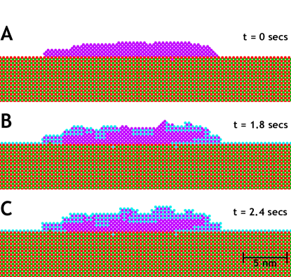
In the low temperature and high As deposition rate regime nucleation of GaAs clusters near the vapor-liquid is significant. This results in the formation of a polycrystalline GaAs shell surrounding a liquid Ga core, as illustrated in Figure 8. In the figure, a liquid droplet grown at is crystallized by an As flux, deposited at a rate of 0.8 ML/s. Nucleation at the vapor-liquid interface occurs within seconds upon crystallization (Figure 8B). The liquid core in the final configuration (C) is completely surrounded by a GaAs shell after 2.4 seconds, preventing any further crystallization of the liquid.
The presence of polycrystalline GaAs, with a high number of grain boundaries and stacking faults that this implies, prevents the possibility that such islands could act as efficient emitters and hence are undesirable. Annealing at higher temperature may remove such defects because grain boundaries and stacking faults provide fast diffusion paths for the liquid Ga trapped within the shell. Such paths are accessible at higher temperatures. Moreover, thermal fluctuations of the nuclei can effectively serve to dissolve the shell, which are characteristically thin in this regime. Therefore such configurations may be annealed at a high temperature to remove defects. Indeed, the simulations bear this out. Figure 9 shows a quantum dot with polycrystalline shell resulting from the crystallization of a liquid droplet at an As deposition rate of ML/s and temperature . The dot is then annealed at a higher temperature . The initial configuration (9A) shows the droplet prior to recrystallization. Temperature is then increased, maintaining the same As flux. Ga atoms move along grain boundaries toward the surface, resulting in a broadening of the dot. The thin shell dissolves, resulting in liquid Ga exposed to As (B, C). Within two seconds, the droplet becomes fully crystallized (D) into a shallow GaAs island, absent of any defects.
These simulations show that liquid cores arising due to nucleation at the vapor-liquid interface, which would be detrimental to optical and electronic properties of quantum dots, can be eliminated by annealing. This expands the parameter space available for the formation of quantum dots formed via droplet epitaxy, allowing the fabrication of optical quality dots even at low temperatures. Even if not strictly related to the presence of a liquid core, but rather to a low quality of the crystalline nature of the fabricated nanostructures, post-crystallization in-situ annealing temperatures have been experimentally demonstrated to strongly increase the optical quality of droplet epitaxy GaAs/AlGaAs dots, reducing individual dot emission linesMano et al. (2009), allowing single photon emission upto liquid nitrogen temperatures Cavigli et al. (2012) and increasing the dot emission decay time.
IV.2.2 Mullins Sekerka Instability
As described above, simulations show that crystallization performed at low temperature and high As flux result in nucleation of polycrystalline GaAs shells surrounding a liquid Ga core, resulting from nucleation of GaAs at the vapor-liquid interface. In the high temperature regime, such surface nucleation does not occur. However, for crystallization at sufficiently high fluxes and high temperature, simulations show the existence of liquid Ga core structures surrounded by GaAs shells in registry with the substrate. As a consequence, such shells are monocrystalline and result from a mechanism separate from surface nucleation.
By examining the formation of such structures in the simulations, we propose that these shells are driven by an instability at the liquid-solid growth front. Simulation snapshots in Figure 10 illustrate the growth mechanism behind this. When this phenomenon occurs no surface nucleation is observed; instead, the growth of the GaAs front undergoes an instability at the liquid-solid interface characterized by unstable undulations of the solid growth front. Such instabilities grow along the droplet-vapor surface until they have completely surrounded the liquid Ga subsequently preventing further crystallization.
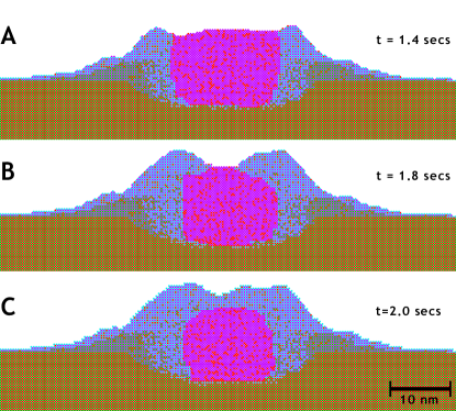
This behavior suggests the presence of a Mullins-Sekerka (MS) instability during crystallization, which implies that only perturbations of sufficiently large wavelength experience unstable growth. Therefore, droplets must be sufficiently large to accommodate perturbations of appropriate wavelength in order for the instability to manifest. The effect of temperature, As flux and droplet radius have on the presence of the MS instability is given in Section V. but the droplet size dependence may be utilized in order to confirm the existence of liquid cores by MS instability experimentally.
It is important to note that simulations suggest that, unlike those formed by surface nucleation, the core-shell structure formed due to the MS instability cannot readily be annealed and recrystallized into an epitaxial nanodot. In this case, shell is in registry with respect to the substrate. Therefore, there are no defects along which liquid Ga can move so that they may crystallize upon exposure to the As vapor. Crystallization of such liquid cores may still occur, however, if the shell is thin enough to dissolve upon annealing thus exposing the liquid Ga to the As flux, however instability-induced shells are characteristically thicker than those resulting from surface nucleation according to simulations.
Experimental Validation. In order to experimentally validate the presence of the MS instability predicted by simulations, nano-islands were formed via droplet epitaxy by depositing Ga droplets of extremely different sizes (60 and 250 nm diameter) and crystallizing them at high As BEP at . Simulations predict a size driven transition from a uniform crystallization for small droplet radii to a Ga rich core at higher droplet sizes. We used Si as the growth substrate. This is dictated by the need of differentiation of the nano-island constituents (Ga and As) from that of the substrate (Si) Somaschini et al. (2010b), thus allowing the use of standard EDS – STEM techniques for the characterization of the As and Ga distribution within the islands. The samples were prepared as follows. Before the introduction into the MBE system, Si(001) substrates were cleaned by standard RCA treatment and finally dipped into HF solution to get the H-termination of the surface, confirmed by the () pattern observed with RHEED. Subsequently, the substrate temperature was set at and the hydrogen desorption was carried out until a mixed () () surface reconstruction was clearly obtained. After this step, the substrate temperature was decreased to either (sample A) or (sample B) for Ga deposition. Here a Ga molecular beam flux was supplied with a deposition rate of 0.075 ML/s and a background pressure below Torr for a total of 3.0 ML of Ga. Finally the crystallization of Ga was achieved at by exposure to an As flux of Torr for 5 minutes. During the As irradiation, the RHEED pattern turned from halo, indicative of liquid droplets, to spotty, signalling the formation of three dimensional structures. However, a clear spotty pattern was not observed for the larger islands.
For TEM observations an FEG (Field Emission Gun) TEM/STEM 2200 FS JEOL instrument operated at 200 kV was used. It was equipped with an energy dispersive X-ray spectrometer (EDS) and an in-column Omega-type Energy Filter. By the latter, elemental maps of Ga and As can be obtained in the energy filtering operation mode of the TEM (EF-TEM). The EF-TEM elemental maps where acquired with a GATAN slow scan CCD camera controlled by the Digital Micrograph software. The maps were obtained by recording the intensity of the L3 absorption edge for Ga (at 1116 eV) and As (at 1323 eV). One post-edge and two pre-edge images were acquired using a slit of 50 eV for both Ga and As. From the two pre-edge images the background image was evaluated which was then subtracted from the post-edge image to get the relevant elemental map. EDS maps were obtained in the STEM operation mode with a spot size of 1 nm and recording the intensity of the L characteristic X-ray emission lines of Ga (1096 keV) and As (1282 keV). The JEOL ultra-thin window Si detector and software were employed for acquisition of the maps. Dead time during measurements was 5-6% and counting time of the order of 8-10 minutes.
The TEM top views of islands from sample A, obtained with diffraction vector clearly show Moiré fringes, due to the interference between the crystal lattice of the island (GaAs) and that the Si substrate (Figure 11). EDS map scans show the same distribution of the Ga and As signals, which mimics the island shape, thus demonstrating the correct stoichiometry of the GaAs all over the island volume – i.e. a fully crystallized island. A different scenario is shown by sample B. Here the nanostructure generated Moiré interference fringes are visible only at the island edges with a featureless center. EDS maps scans show that the distribution of Ga and As are extremely different inside the island (Figure 12). While the Ga signal intensity follows the island profile, As intensity is peaked at the island perimeter with a small, though non-zero, As signal coming from the center. Such a distribution is confirmed by EF-TEM (energy filtered TEM) measurements, and implies a metallic Ga core similar to the one depicted in Figure 10.

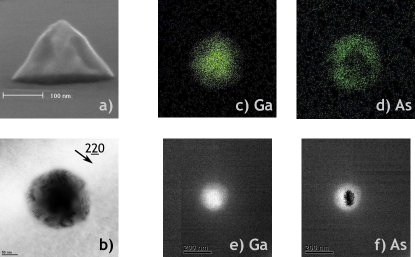
The experiment rules out the presence of a liquid Ga core/ GaAs shell structure by means of surface nucleation due to the fact that the shell is monocrystalline and appears only for the high droplet radius. Nucleation at the liquid-solid interface is predicted to be driven more by the growth temperature and As flux. Because both samples were performed at the same growth conditions, if nucleation driven GaAs shells were to occur, it must occur in both samples. Because this is not the case, we may conclude that the liquid cores observed in the experiments are driven by an MS instability.
V Model Analysis
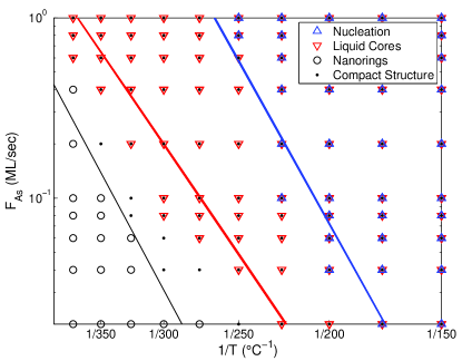
Both simulations and experiments have shown that droplet epitaxy can result in a wide range of morphologies depending on the growth conditions. By varying and , we have established their effect on the resulting nanostructures observed in simulations. From this data, it is clear that compact islands form at low temperature and, as the As overpressure is reduced or the temperature is increased the nanostructures become rings. In cases of large , core-shell structures are observed. The simulation results are summarized in the structural map given in Figure 13. In this section, we will appeal to physical and mathematical arguments to further explain the simulation results. In particular, the solid lines in Figure 13 that delineate the morphological structure will be derived in this section.
We argue that various morphologies observed both in experiments and simulations can be explained in the context of three key processes active during nanostructure formation. In the first Ga atoms in the liquid drop will be “wicked” out of the droplet onto the substrate by capillary-type forces when exposed to an As overpressure. These forces arise as it is energetically favorable for As atoms on the surface to become fully coordinated with Ga atoms. Next, As atoms deposited near or on the droplet diffuse rapidly Gorokhov et al. (1984) through the liquid and attach on a growing GaAs front at the liquid-solid interface, crystallizing the droplet epitaxially. Finally, As atoms may also nucleate near the vapor-liquid interface. These three processes: wicking, crystallization and nucleation are illustrated in Figure 14. The relative rates at which these processes occur depend on growth conditions and will determine the resulting morphology.

V.1 Nanoring Formation
The formation of nanorings is a competition between the wicking and crystallization processes. The crystallization process results in GaAs fronts that grow until the liquid Ga is consumed. If the fronts coalesce before this occurs, the resulting nanostructure is a compact quantum dot. If however, the liquid Ga is consumed before the fronts come together, nanorings result.
To compare the rates of the two processes, we establish expressions for the velocity of the GaAs front as well as the rate at which Ga atoms are wicked out of the droplet. Assuming quasi-static deposition, the velocity of the GaAs front under an As deposition rate scales according to that rate:
| (3) |
where is the atomic spacing of the lattice and is factor that depends shape of the liquid region and possible difference in the As adsorption probability between the droplet itself and its surroundings. For simplicity, . In the wicking process, Ga atoms are driven from the droplet by the deposition of As on the surface away from the droplet. The time scale of the wicking process is given by
| (4) |
while the diffusion length scale is given by
| (5) |
where is the diffusion coefficient of Ga diffusing on a mostly Ga terminated surface, in the presence of As deposition. We have
where was defined in Section II to be a rate prefactor.
The energy barrier eV describing the diffusion of Ga on surface not purely Ga terminated is obtained from the harmonic average of the diffusion rates of Ga-on-Ga diffusion and Ga-on-As diffusion. By prescribing a constant value that describes the effective energetic barrier for diffusion on a mostly Ga-terminated surface, we have assumed that the diffusivity throughout the domain is constant. In reality, diffusivity is spatially dependent due to differences in surface reconstruction near and away from the liquid Ga as observed in micro-RHEED experiments by Isu et al. Isu et al. (1991). This effect is also at the origin of the possibility, offered by droplet epitaxy, to tune ring morphologies Somaschini et al. (2010b). In extreme growth regimes when temperature is less than C and As overpressure greater than Torr, the surface reconstruction may change rapidly even in the proximity of the droplet, implying that the spatial dependence on diffusivity is an important effect. Away from such growth conditions, however, assuming constant effective diffusivity is a reasonable approximation.
Equations (4) and (5) yield a velocity for the wicking of Ga atom from the liquid droplet
| (6) |
A fully crystallized quantum dot forms under conditions where the crystallization process is dominant (). However, if the wicking process is sufficiently fast (), then as described above, the fronts may fail to coalesce, resulting in a nanoring. The critical configuration separating these two scenarios occurs when the crystallization fronts are tangent to each other. To express this critical condition quantitatively, consider the volume of unconsumed liquid Ga at time :
| (7) |
where is a shape constant describing the geometry of the crystallization front (which we model as a quarter-circle) and
is the initial volume of the liquid droplet of radius , being the shape constant that describes the geometry of the droplet. As a first-order approximation, the value of is selected as the average of the shape constant describing a circular and half-circular droplet. The radius of a Ga droplet obtained from the deposition of 4.0 ML of Ga atoms at temperature and flux was found empirically from independent simulations to follow the power law:
| (8) |
where (# atoms) and are empirically obtained values. is the diffusion coefficient for Ga-on-Ga diffusion with corresponding energy barrier eV. The positive root of equation (7) describes the time when all Ga has been consumed. The length of the crystallized front is then given by , and the critical condition may be expressed as
Using equations (8), (3), and (6) , this critical configuration can be written in terms of the growth conditions as
| (9) |
If then compact structures will result on other hand if nanorings will result. Figure 7 illustrates the transition from nanorings to compact quantum dots with increasing . The black line in Figure 13 shows a plot of vs. . The agreement with the simulation data is quite good – it separates compact structures (black dots in the figure) from nanorings (black circles).
A crucial assumption has been made in the argument presented here, namely that no nucleation takes place within the Ga droplet and the crystallizing front moves in a stable fashion (i.e. no Mullins-Sekerka instability occurs). In what follows we shall examine in what regimes in parameter space these factors play an important role.
V.2 Nucleation
Here we will demonstrate that when the As deposition rate is sufficiently large and temperature is low enough, the dominant process will be nucleation at the vapor-liquid interface. As a consequence, the wicking process makes a negligible contribution to the morphology. The rate of the nucleation process at the vapor-liquid interface may be estimated by considering the As concentration within a domain of liquid Ga in contact with a GaAs substrate and As flux. For simplicity we will consider the domain to be rectangular with periodic boundary conditions in the horizontal direction. Assuming quasi-static deposition at a rate ML/s and temperature , the concentration satisfies
where is the equilibrium As concentration above a flat liquid-solid interface and the diffusion coefficient
describes the diffusion of As through liquid Ga, eV being the energy barrier for diffusion throughout the liquid droplet defined earlier in Section II.
The equilibrium concentration is of the form
where are the energy barriers for the detachment and attachment of an As atom in the liquid phase from and onto a flat interface, respectively, defined in Section II. From this diffusion model, the equilibrium concentration at the surface of the droplet is given by
| (10) |
where is the height of the droplet.
Nucleation is most likely to occur where the As concentration is the largest, near the vapor-liquid interface. This means that nucleation will occur when is larger than some critical concentration:
| (11) |
where eV is the nucleation barrier of GaAs in liquid Ga, treated as a fitting parameter. Replacing in equation (10) with the droplet radius , the critical condition (11) for surface nucleation can be expressed in terms of and as:
| (12) |
If the As deposition rate exceeds then GaAs crystallites will form at the vapor-liquid interface, as illustrated in Figure 8. The blue line in Figure 13 is a plot as function of . It accurately predicts the presence of nucleation in simulation results (blue triangles).
V.3 Mullins-Sekerka Instability
In the case where the rates of both the wicking and nucleation processes are negligible, the crystallization process dominates, resulting in the growth of crystallization fronts at the triple point and in registry with the substrate.
As observed in Section IV.2.2, this growth can be unstable due to a Mullins-Sekerka instability leading to GaAs shells epitaxial to the substrate surrounding a liquid Ga core. Perturbations to the planar growth front of sufficiently long wavelength experience this instability, and a standard linear perturbation analysis Bales and Zangwill (1990); Caroli et al. (1992) yields a critical wavelength
where eV is the liquid/solid interfacial energy, obtained directly from the model. In order to accommodate perturbations that experience the MS instability, droplets necessarily must have radius on the order of , i.e. , for some constant . This critical condition may be expressed in terms of and using the above equation along with the model for droplet radius (8):
| (13) |
If then liquid cores will form via a Mullins-Sekerka instability. Figure 13 shows a plot of vs . The scaling constant was selected to best match simulation results, though its specific value do not affect the qualitative shape of the boundary curve, and in particular its slope. The simulation results when a liquid core was observed are plotted as red triangles. We observe that the theoretical curve slightly underestimates the instability within the simulations. This underestimation is inherent to our model and can be attributed to discrete effects. Such effects on nucleation and hence instabilities of the type outlined above are indeed well-studied in the context of diffusion limited aggregation Russo et al. (2004); Witten and Sander (1981).
VI Conclusion
We have presented experimental, simulation and analytical results detailing the precise relationship between growth conditions and the resulting nanostructures formed in droplet epitaxy and crystallization experiments. The KMC model used in conjunction with experiments was presented as an explicitly atomistic, multi-species, multi-phase model capable of simulating all the relevant processes involved with GaAs homoepitaxy, droplet epitaxy and crystallization. As an initial validation, the KMC model accurately reproduces surface termination diagram in the case of GaAs homoepitaxy. We then presented simulation and experimental results of droplet formation and crystallization, exhibiting a qualitative agreement on the resulting morphological dependence on As flux and temperature. Both experiments and simulation suggest a continuum of structures ranging between compact quantum dots to broad nanorings as a function of As flux and temperature. Simulations also suggest the existence of Ga/GaAs core shell structures, as well as elucidating the mechanisms behind their formation. The simulations suggested that a quantum dot with a liquid core could result due to a Mullins-Sekerka instability during the growth of the GaAs front. We presented experiments which validate this hypothesis. In the case of nucleation-driven shells, we provide simulation evidence suggesting that under high temperature annealing, polycrystalline shells may be recrystallized into an epitaxial GaAs island. Lastly, we developed a unifying theory identifying three key processes active during crystallization. It predicts the existence of all the phenomena observed above and their dependence on growth conditions and compares well with empirical simulation data.
VII Acknowledgements
P.S. and K.R. were supported in part by NSF support grants DMS-0854870 and DMS-1115252. D.N. and J.M.M. acknowledge the financial support of the NSF through Grant No. DMR-0906909. S.B., C.S. and S.S. acknowledge the CARIPLO Foundation for financial support (prj. SOQQUADRO - no. 2011-0362)
References
- Kastner (1993) M. Kastner, Physics Today 46, 24 (1993).
- Li and Wang (2003) J. Li and Wang, Nano Letters 3, 1357 (2003).
- Koguchi et al. (1991) N. Koguchi, S. Takahashi, and T. Chikyow, Journal of Crystal Growth 111, 688 (1991).
- Koguchi et al. (1993) N. Koguchi, K. Ishige, and S. Takahashi (1993), vol. 11, pp. 787–790.
- Koguchi and Ishige (1993) N. Koguchi and K. Ishige, Japanese Journal of Applied Physics 32, 2052 (1993).
- Watanabe et al. (2000) K. Watanabe, N. Koguchi, and Y. Gotoh, Japanese Journal of Applied Physics 39, L79 (2000).
- Mano et al. (2005) T. Mano, T. Kuroda, S. Sanguinetti, T. Ochiai, T. Tateno, J. Kim, T. Noda, M. Kawabe, K. Sakoda, G. Kido, et al., Nano Letters 5, 425 (2005).
- Somaschini et al. (2009) C. Somaschini, S. Bietti, N. Koguchi, and S. Sanguinetti, Nano Letters 9, 3419 (2009).
- Somaschini et al. (2012) C. Somaschini, S. Bietti, A. Scaccabarozzi, E. Grilli, and S. Sanguinetti, Crystal Growth and Design 12, 1180 (2012).
- Somaschini et al. (2010a) C. Somaschini, S. Bietti, S. Sanguinetti, N. Koguchi, and A. Fedorov, Nanotechnology 21, 125601 (2010a).
- Somaschini et al. (2011a) C. Somaschini, S. Bietti, N. Koguchi, and S. Sanguinetti, Nanotechnology 22, 185602 (2011a).
- Shitara et al. (1992) T. Shitara, D. D. Vvedensky, M. R. Wilby, J. Zhang, J. H. Neave, and B. A. Joyce, Phys. Rev. B 46, 6815 (1992).
- Kawamura and Ishii (1999) T. Kawamura and A. Ishii, Surface Science 438, 155 (1999).
- Kawamura and Ishii (2001) T. Kawamura and A. Ishii, Surface Science 493, 438 (2001).
- Ishii and Kawamura (1999) A. Ishii and T. Kawamura, Surface Science 436, 38 (1999).
- Somaschini et al. (2010b) C. Somaschini, S. Bietti, N. Koguchi, and S. Sanguinetti, Applied Physics Letters 97, 203109 (2010b).
- Somaschini et al. (2010c) C. Somaschini, S. Bietti, A. Fedorov, N. Koguchi, and S. Sanguinetti, Nanoscale Research Letters 5, 1865–1867 (2010c).
- Chakrabarti et al. (2006) A. Chakrabarti, P. Kratzer, and M. Scheffler, Phys. Rev. B 74, 245328 (2006).
- Orme et al. (1994) C. Orme, M. D. Johnson, J. L. Sudijono, K. T. Leung, and B. G. Orr, Applied Physics Letters 64, 860 (1994).
- Gorokhov et al. (1984) V. Gorokhov, T. Dedegkaev, Y. Ilyin, V. Moshnikov, A. Petrov, Y. Sosov, and D. Yaskov, Crystal Res. and Technol. 19, 1465 (1984).
- Reyes (2013) K. Reyes (2013).
- Biehl (2005) M. Biehl, in Multiscale Modeling in Epitaxial Growth, edited by A. Voigt (2005), vol. 149 of International Series of Numerical Mathematics, pp. 3–18.
- Blue et al. (1995) J. L. Blue, I. Beichl, and F. Sullivan, Phys. Rev. E 51, R867 (1995).
- Ohtake (2008) A. Ohtake, Surface Science Reports 63, 295 (2008).
- Ferguson et al. (1992) I. Ferguson, A. de Oliveira, and B. Joyce, Journal of Crystal Growth 121, 267 (1992).
- Liang and Tu (1993) B. Liang and C. Tu, Journal of Crystal Growth 128, 538 (1993).
- Yamaguchi and Horikoshi (1992) H. Yamaguchi and Y. Horikoshi, Journal of Applied Physics 71, 1753 (1992).
- Wang et al. (2007) Z. M. Wang, B. L. Liang, K. A. Sablon, and G. J. Salamo, Applied Physics Letters 90, 113120 (2007).
- Kuroda et al. (2005) T. Kuroda, T. Mano, T. Ochiai, S. Sanguinetti, K. Sakoda, G. Kido, and N. Koguchi, Phys. Rev. B 72, 205301 (2005).
- Watanabe et al. (2001) K. Watanabe, S. Tsukamoto, Y. Gotoh, and N. Koguchi, Journal of Crystal Growth 227–228, 1073 (2001).
- Kuroda et al. (2002) T. Kuroda, S. Sanguinetti, M. Gurioli, K. Watanabe, F. Minami, and N. Koguchi, Phys. Rev. B 66, 121302 (2002).
- Sanguinetti et al. (2002) S. Sanguinetti, K. Watanabe, T. Tateno, M. Wakaki, N. Koguchi, T. Kuroda, F. Minami, and M. Gurioli, Applied Physics Letters 81, 613 (2002).
- Heyn et al. (2011) C. Heyn, A. Stemmann, M. Klingbeil, C. Strelow, T. Köppen, S. Mendach, and W. Hansen, Journal of Crystal Growth 323, 263 (2011).
- Somaschini et al. (2011b) C. Somaschini, S. Bietti, A. Fedorov, N. Koguchi, and S. Sanguinetti, Journal of Crystal Growth 323, 279 (2011b).
- Mano et al. (2009) T. Mano, M. Abbarchi, T. Kuroda, C. A. Mastrandrea, A. Vinattieri, S. Sanguinetti, K. Sakoda, and M. Gurioli, Nanotechnology 20, 395601 (2009).
- Cavigli et al. (2012) L. Cavigli, S. Bietti, N. Accanto, S. Minari, M. Abbarchi, G. Isella, C. Frigeri, A. Vinattieri, M. Gurioli, and S. Sanguinetti, Applied Physics Letters 100, 231112 (2012).
- Isu et al. (1991) T. Isu, M. Hata, and A. Watanabe, Journal of Crystal Growth 111, 210 (1991).
- Bales and Zangwill (1990) G. S. Bales and A. Zangwill, Phys. Rev. B 41, 5500 (1990).
- Caroli et al. (1992) B. Caroli, C. Caroli, and B. Roulet, in Solids far from equilibrium, edited by C. Godréche (Cambridge University Press, 1992), pp. 155–296.
- Russo et al. (2004) G. Russo, L. M. Sander, and P. Smereka, Phys. Rev. B 69, 121406 (2004).
- Witten and Sander (1981) T. A. Witten and L. M. Sander, Phys. Rev. Lett. 47, 1400 (1981).