Electrical Control of Optical Properties of Monolayer MoS2
Abstract
We investigate electrical gating of photoluminescence and optical absorption in monolayer molybdenum disulfide (MoS2) configured in field effect transistor geometry. We observe an hundredfold increase in photoluminescence intensity and an increase in absorption at nm in these devices when an external gate voltage is decreased from +50 V to -50 V, while the photoluminescence wavelength remains nearly constant. In contrast, in bilayer MoS2 devices we observe almost no changes in photoluminescence with gate voltage. We propose that the differing responses of the monolayer and bilayer devices are related to the interaction of the excitons in MoS2 with charge carriers.
Materials with electrically controllable optical properties find uses in diverse applications ranging from electro-optical modulators to display screens. Unfortunately, the optical constants of most bulk semiconducting materials do not vary significantly with electric field. In the case of silicon, for instance, the variation in refractive index with gate voltage is smaller than , limiting the footprint and the modulation depth of electro-optical modulatorsLiu et al. (1997). While larger electro-optical response has been demonstrated in other semiconductors, such as germanium and gallium arsenide, integration of these materials with silicon CMOS fabrication may prove difficultMiller et al. (1997); Kuo et al. (2005). Very recently, two-dimensional (2D) atomic crystalsNovoselov et al. (2005) emerged as a potential alternative to bulk semiconductors for photonic applicationsBonaccorso et al. (2005). In graphene, the most widely studied 2D material, changes in optical absorption larger than produced by the electric field effect have been used to demonstrate nanoscale electro-optical modulators in the infrared rangeLiu et al. (2005). However, the lack of a band gap in graphene makes its uses at visible frequencies infeasible.

Here we demonstrate electrical control of photoluminescence quantum yield and absorption coefficient in the visible range for a different two-dimensional crystal, monolayer molybdenum disulfide (MoS2). This material consists of a layer of molybdenum atoms surrounded by sulfur in a trigonal prismatic arrangementYoffe et al. (2005) (Fig. 1d, Inset). Unlike semi-metallic graphene, monolayer MoS2 (1xMoS2) is a semiconductor with a direct band gap of eV, and is therefore optically active in the visible rangeMak et al. (2005); Splendiani et al. (2005). The combination of a substantial band gap and high ( cm2/Vs) carrier mobility Radisavljevic et al. (2005) invites electro-optic applications of MoS2. Finally, monolayer MoS2 can be synthesized using several scalable methods potentially compatible with standard CMOS technologyLee et al. (2005). We fabricate monolayer MoS2 field effect transistors (FETs) and probe changes in their optical properties in response to an externally applied gate voltage (). At =-50 V, we observe a bright photoluminescence (PL) band centered at eV that decreases in intensity by more than a factor of 100 as is swept from -50 V to 50 V. Concurrently, we observe a decrease in absorption at the same wavelength. We propose that these phenomena are caused by the interaction of excitons in MoS2 with conduction electrons via the phase-space filling effect.
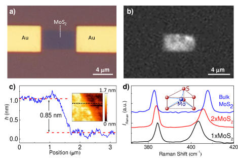
We have fabricated FETs by first depositing monolayer and bilayer MoS2 flakes with average dimensions of several microns onto SiO2/Si substrates via micromechanical exfoliationNovoselov et al. (2005). Individual MoS2 flakes are contacted electrically using metal electrodes deposited via electron beam lithography followed by thermal metal evaporation (Fig. 1a). While Cr/Au and Ti/Au contacts were used, we found that Au electrodes without any wetting layer produced the least contact resistance Popov et al. (2005). Altogether we fabricated eight monolayer MoS2 (1xMoS2) FETs that showed similar electrical and optical characteristics. We also fabricated two bilayer MoS2 (2xMoS2) devices. We confirmed the monolayer character of the 1xMoS2 samples in three different ways. First, we investigated the fluorescence microscopy images of the devices, since bright fluorescence only occurs for monolayer MoS2, and is a signature of a direct band-gap material (Fig. 1b)Mak et al. (2005); Splendiani et al. (2005). Second, contact-mode atomic-force microscopy (AFM) measurements confirm that our devices are less than 1 nm thick, comparing favorably to the expected value of nm (Fig. 1c) Lee et al. (2005). Finally, Raman spectra of our devices exhibit characteristic and peaks that are spaced 19 cm-1 apart, a characteristic signature of monolayer MoS2 flakes (Fig. 1d)Lee et al. (2005). The bilayer character of MoS2 in the 2xMoS2 devices was also confirmed by Raman spectroscopy, fluorescence microscopy and AFM.
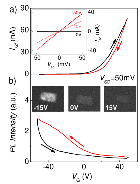
We first measured electrical transport in a typical 1xMoS2 device in ambient dark environment at room temperature. The source-drain current-voltage curve, , remains linear for mV (Fig. 2a, Inset), indicating good electrical contact to the device and the lack of any Schottky barriers at the electrode-MoS2 interface Radisavljevic et al. (2005). The conductance in this device can be controlled by an externally applied gate voltage , due to the electric-field effect in MoS2 (Fig. 2a). The conductivity increase for V proves that the device is operating in the electron-doping regime, while near-complete suppression of conductivity for V is consistent with the larger than band gap of MoS2 Radisavljevic et al. (2005). For device , we estimate the field-effect mobility cm2/Vs, where and are the length, width and resistance of the device, respectively and aF m-2 is the geometrical capacitance between MoS2 and the silicon back gate. For other devices, we observed mobilities in the range cm2/Vs.

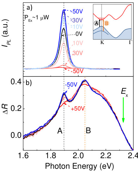
Simultaneously with electrical measurements, we studied photoluminescence of the devices, both via conventional fluorescence microscopy, and by using scanning confocal microscopy with laser excitation wavelength at nm (2.33 eV), power ranging between W, and with a diffraction-limited spot size of m. At zero gate voltage we observe bright luminescence at eV (feature “A”, Fig. 3a), a feature previously observed both in monolayer Mak et al. (2005); Splendiani et al. (2005); Eda et al. (2005) and bulk Yoffe et al. (2005) MoS2. This feature has been attributed to the recombination of photoexcited excitons across the direct band gap at the K-point (Fig. 3a, Inset).

Crucially, in every device, the PL intensity changes dramatically with gate voltage. When is increased, with a concomitant increase in conductivity, the intensity of the PL (integrated area under the peak) diminishes (Fig. 2b). In the range of gate voltages between +50 V and -50 V, the maximum PL intensity changes by more than factor of 12 for that device. Gate-dependent variation in the PL intensity up to has been observed for other devices, such as device (Fig. 3a). This variation was found to be fully reversible, reproducible over months of measurements, and persistent in the entire range of excitation powers (Supplementary Information, Fig. S2).
Next, we focus on the absorption coefficient of monolayer MoS2 and investigate its possible dependence on the gate voltage . We accomplish this by measuring differential reflectivity of our devices, where and is the reflectivity of the MoS2 specimen on SiO2/Si substrate (bare substrate next to MoS2). We observe a prominent peak in at an energy corresponding to the feature “A” in the PL spectrum and an additional peak “B” at eV (Fig. 3b). These features correspond to excitonic transitions between the valence band split by spin-orbit interaction and the conductance band (Fig. 3a, Inset) Splendiani et al. (2005). Crucially, we find that while both “A” and “B” peaks in depend on gate voltage, away from these peaks is -independent. Since and are interrelated Forker et al. (2005), we conclude that absorption is constant away from “A” and “B” peaks.

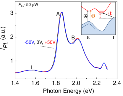
Finally, we investigate the -dependence of PL for a bilayer MoS2, an indirect band gap material Mak et al. (2005); Splendiani et al. (2005). For V, we observe features “A” and “B”, similar to those seen in single-layer MoS2, along with an appearance of a broad lower-energy feature “I” at eV (Fig. 4). We use larger excitation power W since the overall luminescence yield in these devices is significantly lower than that from monolayer MoS2 Splendiani et al. (2005). (Data taken using smaller excitation power are presented in Supplementary Figure S5). These spectral features are related to the band structure of 2xMoS2 (Fig. 4, Inset). The low-intensity feature “I” is associated with momentum-violating phonon-assisted transition across the indirect band gapMak et al. (2005); Splendiani et al. (2005). Calculations predict that the band structure near the K-point and hence excitons “A” and “B” is only weakly affected by quantum confinement and is similar between single- and bilayer MoS2. The comparable intensities of both features “A” and “B” in 2xMoS2 are also unsurprising, since in 2xMoS2 both of these transitions result from hot luminescence. Crucially, for 2xMoS2 we observe no changes larger than in either feature “A” and “B” in the accessible range of (Fig. 4 and Fig. S5).
Summarizing the discussion so far, our main experimental findings are i) large variation of both PL intensity and optical absorption with gate voltage for monolayer MoS2, and ii) the lack of substantial PL variation for bilayer MoS2. We now focus on elucidating the mechanism of these phenomena.
First, the observed changes in PL intensity are not a result of electroluminescence Noborisaka et al. (2011). Measured photoluminescence is relatively constant across the devices area, does not depend on the bias voltage applied to MoS2, and was observed for zero bias current. Second, the observed changes in PL intensity are not caused by changes in absorbance of MoS2 at the excitation frequency. Indeed, since does not vary with at the excitation energy eV (Fig. 3b), away from “A” and “B” peaks, absorption coefficient eV) must be independent of gate voltage. This result is expected: in the measured gate voltage range V, the expected change in the carrier density due to the field effect is cm-2. This change in the carrier density translates into a shift of the Fermi energy by meV, where m is the effective electron mass in 1xMoS2 ( assuming spin degeneracy for the conduction band)Cheiwchanchamnangij et al. (2005). This shift is small compared to the difference between fluorescence (1.85 eV) and excitation (2.33 eV) energies. Therefore, an electrostatically induced shift of the Fermi energy cannot affect the absorption at the excitation wavelength, opposite to what is observed for graphene in the infrared rangeWang et al. (2005).
Next, we consider the possible contribution of sample disorder. In principle, defects and disorder in a material can localize both charge carriers and excitons, which, in turn, can result in gate-voltage-dependent photoluminescence Finkelstein et al. (2005). To analyze this scenario, we compared PL data from different samples with mobility ranging from 0.1 cm2/Vs to 13 cm2/Vs. Despite over two orders of magnitude variation in carrier mobility between samples, curves were similar for every measured device, with less than a factor of two variation of PL intensity recorded at V between different samples (see Supplementary Material, Fig. S3). While we did observe larger variation of PL intensity between devices at V (such as Devices and ), this variation can be ascribed to difference in unintentional doping levels between the samples resulting from interactions with the substrate Shi et al. (2009). We therefore believe that the mechanism responsible for gate-voltage-dependent PL intensity is intrinsic rather than extrinsic in nature and is primarily related to the interaction of excitons in MoS2 with free charge carriers.
We now suggest a possible mechanism for this interaction, the phase-space filling effect Schmitt-Rink et al. (2005). In this mechanism, an increase of the carrier density renders part of a phase space unavailable for exciton formation due to Pauli exclusion principle. This causes a reduction in the exciton oscillator strength and a corresponding decrease of PL intensity and excitonic absorption. A simple estimate Schmitt-Rink et al. (2005) predicts that the PL intensity will be halved at the critical carrier density cm-2, where nm is an effective Bohr radius for an exciton Cheiwchanchamnangij et al. (2005). While this density is an order of magnitude larger than the variation of the carrier density cm-2 in our experiment, it is possible that this deviation is caused either by inaccuracies in the estimated exciton radius stemming from uncertainty in the dielectric constant of MoS2 (for a monolayer MoS2, the effective dielectric constant could be affected by either the underlying substrate or by the impurities on the surface of MoS2) or by effects related to nonuniform doping profiles in the devices. Furthermore, the phase-space filling mechanism is consistent with the absence of gate-dependent changes in PL in bilayer MoS2. Indeed, for 2xMoS2, the excitons and the conductions electrons occupy different regions of the phase space. The one-particle states participating in the formation of “A” and “B” excitons have momenta near the K-point, whereas conduction electrons reside across the indirect gap, away from the K-point (Fig. 4, Inset). Therefore, changes in the carrier density should not affect the excitonic absorption and PL intensity for 2xMoS2.
In summary, we have demonstrated that both photoluminescence and absorption of monolayer MoS2 at eV can be controlled by gate voltage. We propose that this effect in MoS2 is due to the interaction of excitons with charge carriers and suggest a possible mechanism for such an interaction through the phase-space filling effect. We expect that time-dependent PL measurements, as well as measurements at cryogenic temperatures will elucidate the origin of the observed phenomena Korn et al. (2005).
We envision multiple potential applications for monolayer devices of this type. First, the optical readout of the electronic states of MoS2 transistors can be employed to investigate the nature of conduction in this material and to realize various optoelectronic devices. Second, electrically controlled absorption of light and photoluminescence in high-mobility MoS2 can be utilized to create nanoscale electro-optical modulators operating in the visible range. Finally, we envision the possibility of controlling absorption and fluorescence wavelength in similar devices by exploiting other monolayer materials from the dichalcogenide family, such as MoSe2, WS2 and many others Yoffe et al. (2005).
Acknowledgements: KIB acknowledges the support through NSF CAREER DMR-1056859 and NSF EPS 1004083. JIZ and RFH acknowledge support from the Defense Threat Reduction Agency (HDTRA1-1-10-0047). Samples for this work were prepared at the Vanderbilt Institute of Nanoscale Science and Engineering using facilities renovated under NSF ARI-R2 DMR-0963361. We gratefully acknowledge Kirill A. Velizhanin, Sokrates Pantelides, Leonard Feldman, Arend van der Zande for useful discussions and Hiram Conley for technical assistance.
References
- Liu et al. (1997) A. S. Liu, R. Jones, L. Liao, D. Samara-Rubio, D. Rubin, O. Cohen, R. Nicolaescu, and M. Paniccia, Nature 427, 6975 (2004).
- Miller et al. (1997) D. A. B. Miller, D. S. Chemla, T. C. Damen, A. C. Gossard, W. Wiegmann, T. H. Wood, and C. A. Burrus, Phys. Rev. Lett. 53, 2173 (1984).
- Kuo et al. (2005) Y. H. Kuo, Y. K. Lee, Y. S. Ge, S. Ren, J. E. Roth, T. I. Kamins, D. A. B. Miller, and J. S. Harris, Nature 437, 1334 (2005).
- Novoselov et al. (2005) K. S. Novoselov, D. Jiang, F. Schedin, T. J. Booth, V. V. Khotkevich, S. V. Morozov, and A. K. Geim, P Natl Acad Sci USA 102, 10451 (2005).
- Bonaccorso et al. (2005) F. Bonaccorso, Z. Sun, T. Hasan, and A. C. Ferrari, Nat Photonics 4, 611 (2010).
- Liu et al. (2005) M. Liu, X. B. Yin, E. Ulin-Avila, B. S. Geng, T. Zentgraf, L. Ju, F. Wang, and X. Zhang, Nature 474, 64 (2011).
- Yoffe et al. (2005) A. D. Yoffe, Ann. Rev. Mater. Sci. 3, 147 (1973).
- Mak et al. (2005) K. F. Mak, C. Lee, J. Hone, J. Shan, and T. F. Heinz, Phys. Rev. Lett. 105, 136805 (2010).
- Splendiani et al. (2005) A. Splendiani, L. Sun, Y. B. Zhang, T. S. Li, J. Kim, C. Y. Chim, G. Galli, and F. Wang, Nano Lett. 10, 1271 (2010).
- Radisavljevic et al. (2005) B. Radisavljevic, A. Radenovic, J. Brivio, V. Giacometti, and A. Kis, Nat Nanotechnol 6, 147 (2011).
- Lee et al. (2005) Y. H Lee, X. Q. Zhang, W. J. Zhang, M. T. Chang, C. T. Lin, K. D. Chang, Y. C. Yu, J. T. W. Wang, C. S. Chang, L. J. Li, and T. W. Lin, Adv Mater 24, 2320 (2012).
- Popov et al. (2005) I. Popov, G. Seifert, and D. Tomanek, Phys. Rev. Lett. 108, 156802 (2012).
- Lee et al. (2005) C. Lee, H. Yan, L. E. Brus, T. F. Heinz, J. Hone, and J. Ryu, Acs Nano 4, 2695 (2010).
- Eda et al. (2005) G. Eda, H. Yamaguchi, D. Voiry, T. Fujita, M. W. Chen, and M. Chhowalla, Nano Lett. 11, 5111 (2011).
- Forker et al. (2005) R. Forker, M. Gruenewald, and T. Fritz, Annu. Rep. Prog. Chem. Sect. C: Phys. Chem. 108, 34 (2012).
- Noborisaka et al. (2011) J. Noborisaka, K. Nishiguchi, Y. Ono, H. Kageshima, and A. Fujiwara, App. Phys. Lett. 98, 033503 (2011).
- Cheiwchanchamnangij et al. (2005) T. Cheiwchanchamnangij, and W. R. L. Lambrecht, Phys. Rev. B 85, 205302 (2012).
- Wang et al. (2005) F. Wang, Y. B. Zhang, C. S. Tian, C. Girit, A. Zettl, M. Crommie, and Y. R. Shen, Science 320, 206 (2008).
- Finkelstein et al. (2005) G. Finkelstein, H. Shtrikman, and I. Bar-Joseph, Phys. Rev. Lett. 74, 976 (1995).
- Shi et al. (2009) Y. Shi, X. Dong, P. Chen, J. Wang, and L. Li, Phys. Rev. B 79, 115402 (2009).
- Schmitt-Rink et al. (2005) S. Schmitt-Rink, D. S. Chemla, and D. A. B. Miller, Phys. Rev. B 32, 6601 (1985).
- Korn et al. (2005) T. Korn, S. Heydrich, M. Hirmer, J. Schmutzler, and C. Schuller, App. Phys. Lett. 99, 102109 (2011).