Self-aligned graphene field-effect transistors with polyethyleneimine doped source/drain access regions
Abstract
We report a method of fabricating self-aligned, top-gated graphene field-effect transistors (GFETs) employing polyethyleneimine spin-on-doped source/drain access regions, resulting in a 2X reduction of access resistance and a 2.5X improvement in device electrical characteristics, over undoped devices. The GFETs on Si/SiO2 substrates have high carrier mobilities of up to 6,300 cm2/Vs. Self-aligned spin-on-doping is applicable to GFETs on arbitrary substrates, as demonstrated by a 3X enhancement in performance for GFETs on insulating quartz substrates, which are better suited for radio frequency applications.
pacs:
85.30.Tv, 72.80.LeGraphene’s exceptional electronic properties, in particular its high carrier mobility Geim and Novoselov (2007), high saturation velocity Neto et al. (2009) and large current density Barreiro et al. (2009) make it an excellent channel material for future ultra-high-speed electronic devices. Graphene field-effect transistors (GFETs) have recently attracted significant attention for potential radio frequency (RF) applications, Koswatta et al. (2011) with reports of RF GFETs operating at intrinsic cut-off frequencies up to 300 GHz Liao et al. (2010a). However, theoretical calculations predict GFETs to be capable of running at THz operating frequencies Liao et al. (2010b). One of the major factors preventing optimal THz RF performance of GFETs is high series resistance of the access regions between the source/drain electrodes and the top-gated graphene channel. This parasitic access resistance reduces device drive currents (ID) and transconductances (gm), thereby directly affecting GFET performance. Electrostatic modulation of the access regions is one way of reducing this resistance for devices on heavily doped substrates Lin et al. (2010). This approach requires a global, conducting back-gate and does not provide for independent control of multiple devices on the same substrate, and is unsuitable for GFETs on insulating substrates. This problem can be addressed by fabricating GFETs with self-aligned gates, where the access region dimensions and consequently their resistances are reduced. Previous methods of self-aligned GFET fabrication are not straightforward, and either use physically assembled nanowire gates Liao et al. (2010a), or require pristine quality graphene and ultra high vacuum metal-deposition Farmer, Lin, and Avouris (2010), or restrict scaling of the top-gate dielectric Badmaev et al. (2012). In this work, we present a simple and scalable approach of fabricating self-aligned GFETs, exploiting the unique property of charge-transfer doping of graphene using polyethyleneimine (PEI).
The problem of high access resistance in conventional Si complementary metal-oxide-semiconductor (CMOS) transistors is overcome by heavily doping the source/drain access regions through ion implantation Bower and Dill (1966). We employed a similar approach in this work, by using charge-transfer doping of graphene with PEI D. B. Farmer and R. G. Mojarad and V. Perebeinos and Y. M. Lin and G. S. Tulevski and J. C. Tsang and P. Avouris (2009), to dope the access regions and reduce their resistance. We chose PEI due to its ease of application, but any other method of doping (substitutional, surface-transfer, Liu, Liu, and Zhu (2011) etc.) can, in principle, be used for the same result. We fabricated top-gated GFETs with exposed source/drain access regions and doped them with PEI in a self-aligned manner using a controllable method of spin-on-doping. The fabrication process is universally applicable to GFETs on arbitrary substrates and is specifically demonstrated for GFETs on Si/SiO2 and quartz substrates.

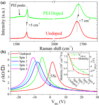
PEI spin-on-doping of graphene was characterized on back-gated GFETs. Monolayer graphene was exfoliated onto highly-doped n-type Si substrates with a 285 nm thermally grown SiO2 layer acting as the back-gate dielectric. Graphene active regions were patterned by e-beam lithography (EBL) and oxygen plasma etching. A second EBL step was performed to define metal contacts for 4-point probe structures, followed by e-beam evaporation of a 50 nm Ni layer as contact metal and a final lift-off. The branched PEI (Sigma Aldrich, 60,000, 750,000) molecular dopants were applied by spin-coating a dilute solution of PEI in methanol onto the substrate. A solution of 0.02% (by wt.) PEI in methanol was prepared by magnetic stirring in a dark, air-tight container for a period of 48 hours. Methanol was used as a solvent due to its high volatility which minimizes solvent residue on the graphene surface. To dope the graphene, this dopant solution was spin-coated onto the GFETs at 1500 rpm for 60 s, followed by a quick bake at 90∘C for 20 s to drive away any remaining methanol residue. PEI, being a heavy macromolecule does not evaporate, but forms a thin adsorbed layer on the graphene, thereby doping it. Figure 1 (a) shows the schematic and Fig. 1 (b) the optical micrograph of a back-gated GFET after spin-on-doping. PEI-doped graphene has a thin, uniform layer of dopants adsorbed on it and cannot be optically distinguished from clean, undoped graphene.

Figure 2 (a) compares the Raman spectra of graphene before and after PEI-doping. The spectrum before doping is indicative of monolayer graphene with a 2D-to-G peak intensity ratio, / of 2.5 and a 2D band full width at half maximum (FWHM) of 25 cm-1 Gupta et al. (2006). Peaks around 1500 cm-1 appear in the Raman spectrum after doping. These peaks indicate the presence of PEI and have been previously reported on carbon nanotube/PEI composite fibers Muñoz et al. (2005). Reduction in the / ratio to 1.5 and an upshift of both the G and 2D peaks is a further indication of n-dopingCasiraghi et al. (2007); Das et al. (2008). The PEI molecules are weakly bonded to the graphene surface and are prone to slow desorption under ambient conditions D. B. Farmer and R. G. Mojarad and V. Perebeinos and Y. M. Lin and G. S. Tulevski and J. C. Tsang and P. Avouris (2009). However, the dopants can be sealed on the graphene surface using an atomic layer deposition (ALD) oxide capping layer to prevent desorption and ensure long-term stability of doping Farmer et al. (2009).
Control of the doping dose was achieved by repetitive spin-on-doping steps. Figure 2 (b) shows 4-point resistivity measurements of the back-gated GFET after successive PEI spin-on-doping steps. The undoped GFET shows a Dirac point (VDIRAC) at + 3 V, likely due to unintentional doping by water vapor during the fabrication process Novoselov et al. (2004). VDIRAC shifts to - 5 V after the first spin-on-doping step, signifying n-type doping due to PEI. Successive spin-on-doping steps increasingly dope the graphene n-type, as evident from shifts in VDIRAC to larger negative voltages after every spin. Carrier mobilities were extracted using a well-established field-effect mobility model Kim et al. (2009) and plotted along with VDIRAC after every spin-on-doping step in Fig. 2 (b) (inset). There is a reduction in carrier mobility with each spin-on-doping step, in accordance with previous reports of dopant induced mobility degradation D. B. Farmer and R. G. Mojarad and V. Perebeinos and Y. M. Lin and G. S. Tulevski and J. C. Tsang and P. Avouris (2009). However, the mobility after four spin-on-doping steps still remains high at 6,000 cm2/Vs. An important effect of doping is reduction in the graphene resistivity at VBG = 0 V from 4.5 k to 1.5 k, a factor of 3X. This reduction in resistivity when employed to the source/drain access regions of a top-gated GFET can result in improved GFET performance.

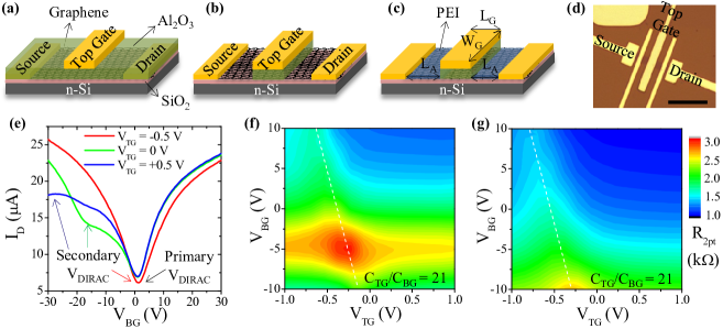
To test this hypothesis, dual-gated GFETs were fabricated on clean, back-gated GFETs by patterning a top-gate stack. A 20 nm ALD Al2O3 layer, seeded by a 15 evaporated Al layer, was deposited as the top-gate dielectric Kim et al. (2009). This was followed by a final EBL step to pattern the top-gate electrode. A 50 nm Ni layer was subsequently deposited as the top-gate metal contact. The source/drain access regions of the GFET at this stage were covered by the ALD Al2O3 layer, which was etched away in order to dope them. This etch was performed in a self-aligned manner using a 1:50 dilute HF solution as the etchant. The top-gate metal acts as a self-aligned hard mask during the etch and protects the top-gate dielectric. It has to be noted that the HF solution etches the underlying SiO2 layer too, albeit at a much slower rate (5 nm/min.) than the ALD Al2O3 top-gate dielectric (60 nm/min.). The etch could thus be conveniently timed to minimize etching of the SiO2 layer. The access regions were then finally spin-on-doped using PEI. Figures 3 (a)-(c) illustrate the fabrication of self-aligned spin-on-doped GFETs and Fig. 3 (d) shows an optical micrograph of the finished top-gated GFET.
The drain current (ID) profiles of a GFET after self-aligned etching, but prior to spin-on-doping, as a function of the back-gate bias (VBG), at different top-gate biases (VTG) are shown in Fig. 3 (e). The profile at VTG = 0 V shows two VDIRAC: a primary VDIRAC at 0 V and a secondary VDIRAC at -17 V. The primary VDIRAC arises from the source/drain access regions and the secondary VDIRAC from the top-gated graphene region. The n-type doping of the top-gated graphene is unintentional, and is probably due to impurities in the ALD Al2O3 layer. The position of the secondary VDIRAC can be selectively modulated using the top-gate bias. A negative VTG (= -0.5 V) depletes electrons from the top-gated graphene region and shifts the secondary VDIRAC close to 0 V, which, in turn, overlaps with the primary VDIRAC to result in one “apparent” VDIRAC for the entire graphene. A positive VTG (= +0.5 V), on the other hand, induces excess electrons in the top-gated graphene region and shifts its VDIRAC to a more negative voltage, beyond - 30 V in this case, as evident from the downturn of ID around - 30 V. The primary VDIRAC is unaffected by the top-gate bias, signifying that the Dirac points of the top-gated graphene and the access regions can be modulated independent of each other.
Selective spin-on-doping of the GFETs was done only in the exposed source/drain regions using 0.02% PEI, while the top-gated graphene region was protected by the top-gate stack. Figures 3 (f) and (g) show the resistance contour plot of the device as a function of VTG and VBG before the self-aligned etch and after self-aligned doping. The only effect of self-aligned doping is to dope the access regions n-type and shift their VDIRAC to a negative voltage. This is evident as an apparent downward shift of the resistance profile along the VBG axis after doping. The resistance profile along the VTG axis remains the same before and after doping, signifying that there is no effect of doping on the top-gated graphene region. The dashed lines represent contours of charge neutrality for the top-gated channel and their slope gives the ratio of the top-gate capacitance to the back-gate capacitance, CTG/CBG = 21. Using the back-gate capacitance value of CBG = 11 nF/cm2, the top-gate capacitance is estimated to be CTG 236 nF/cm2. This corresponds to a relative dielectric constant of 5.7 for the Al2O3 film, which agrees with reports from literature for ALD Al2O3 films on graphene Fallahazad et al. (2012). The slope remains unchanged after the self-aligned etch and doping, thereby indicating no degradation of dielectric properties.

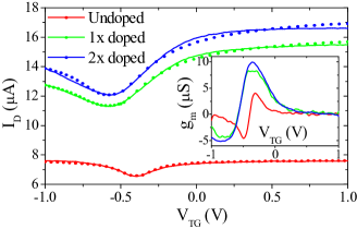
The properties of a GFET with a top-gated channel length, LG = 1.0 m, channel width, WG = 7.0 m and access region length, LA = 1.5 m, before and after two self-aligned doping steps with 0.02% PEI are shown in Fig. 4. The transfer characteristics show an improvement in the maximum drive current (ID,max) from 7.4 A to 16.6 A and in the peak transconductance (gm,max) from 4.2 S to 10.3 S after two spins, an approximately 2.5X improvement. The ION/IOFF ratio also improves by 20% after two spins. To extract the reduction in access resistance, the resistance profiles of the GFET () are fit to the expression,
| (1) |
where is the electron charge, is the field-modulated carrier concentration, is the residual carrier concentration at the neutrality point, and is the field-effect mobility of the top-gated graphene region Kim et al. (2009). is the total series resistance contribution from the source/drain contacts, and access regions, ; = + . The undoped device shows a 6,800 cm2/Vs, which reduces to 6,300 cm2/Vs after doping. reduces from 2.6 k to 1.5 k after one spin, and further down to 1.1 k after two spins. This reduction in is primarily from reduction of . It has to be noted that, in addition to improving the device characteristics, self-aligned spin-on-doping can be used as a knob to tune the ID of a GFET post-fabrication, by varying the doping dose. This method of tuning ID can be particularly useful to compensate for device-to-device variability in graphene integrated circuits Berdebes et al. (2011).

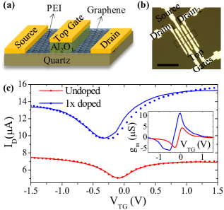
The full advantage of self-aligned spin-on-doping is realized on GFETs on insulating substrates, where the absence of a back-gate makes it impossible to electrostatically modulate the access region resistanceKim et al. (2009). Insulating substrates are also better suited for RF applications due to their lower parasitic capacitances. We specifically chose single crystal quartz substrates, since they are ideal for low loss, temperature stable high-frequency electronics Ramon et al. (2012). To fabricate GFETs on quartz, monolayer graphene was first exfoliated on Si/SiO2 substrates and transferred onto quartz using a poly(methyl methacrylate) based transfer method Kim et al. (2011). Subsequent processing was similar to the processing used for fabricating top-gated GFETs on Si/SiO2 substrates.
Transfer characteristics of a top-gated GFET on quartz, before and after self-aligned doping using 0.02% PEI are shown in Fig. 5. The device dimensions are: LG = 2.0 m, WG = 7.0 m and LA = 1.8 m. The gains in device performance are similar to the GFET on Si/SiO2. ID,max improves from 6.8 A to 15.3 A and gm,max from 4.3 S to 13.1 S, a 3 X improvement. A carrier mobility of 5,600 cm2/Vs is extracted for the undoped device, which reduces slightly to 5,200 cm2/Vs after doping. These values are comparable to the GFET on Si/SiO2 and indicate that quartz can be an attractive insulating substrate for graphene electronics.
In summary, we have demonstrated a simple and controllable method of spin-on-doping graphene using PEI as a chemical dopant. Control of the doping dose was achieved by repetitive spin-on-doping steps. We fabricated dual-gated GFETs on Si/SiO2 substrates and spin-on-doped their access regions in a self-aligned manner to reduce their resistance and improve device performance by up to 2.5X. Further, we fabricated GFETs on insulating quartz substrates and spin-on-doped their access regions, which enhanced their device characteristics by up to 3X. These results indicate that chemical doping of the source/drain access regions can be a viable method of improving GFET performance on arbitrary substrates.
This work was supported by NRI-SWAN and the NSF NASCENT center. We thank D. Ferrer for help with TEM imaging.
References
- Geim and Novoselov (2007) A. K. Geim and K. S. Novoselov, Nat. Mater. 6, 183 (2007).
- Neto et al. (2009) A. H. C. Neto, F. Guinea, N. M. R. Peres, K. S. Novoselov, and A. K. Geim, Rev. Mod. Phys. 81, 109 (2009).
- Barreiro et al. (2009) A. Barreiro, M. Lazzeri, J. Moser, F. Mauri, and A. Bachtold, Phys. Rev. Lett. 103, 076601 (2009).
- Koswatta et al. (2011) S. O. Koswatta, A. V. Garcia, M. B. Steiner, Y. M. Lin, and P. Avouris, IEEE Trans. Microwave Theory Tech. 59, 2739 (2011).
- Liao et al. (2010a) L. Liao, Y. C. Lin, M. Bao, R. Cheng, J. Bai, Y. Liu, Y. Qu, K. L. Wang, Y. Huang, and X. Duan, Nature 467, 305 (2010a).
- Liao et al. (2010b) L. Liao, J. Bai, R. Cheng, Y. C. Lin, S. Jiang, Y. Qu, Y. Huang, and X. Duan, Nano Lett. 10, 3952 (2010b).
- Lin et al. (2010) Y. M. Lin, H. Y. Chiu, K. A. Jenkins, D. B. Farmer, P. Avouris, and A. V. Garcia, IEEE Electron Dev. Lett. 31, 68 (2010).
- Farmer, Lin, and Avouris (2010) D. B. Farmer, Y. M. Lin, and P. Avouris, Appl. Phys. Lett. 97, 013103 (2010).
- Badmaev et al. (2012) A. Badmaev, Y. Che, Z. Li, C. Wang, and C. Zhou, ACS Nano 6, 3371 (2012).
- Bower and Dill (1966) R. W. Bower and R. G. Dill, IEDM 12, 102 (1966).
- D. B. Farmer and R. G. Mojarad and V. Perebeinos and Y. M. Lin and G. S. Tulevski and J. C. Tsang and P. Avouris (2009) D. B. Farmer and R. G. Mojarad and V. Perebeinos and Y. M. Lin and G. S. Tulevski and J. C. Tsang and P. Avouris, Nano Lett. 9, 388 (2009).
- Liu, Liu, and Zhu (2011) H. Liu, Y. Liu, and D. Zhu, J. Mater. Chem. 21, 3335 (2011).
- Gupta et al. (2006) A. Gupta, G. Chen, P. Joshi, S. Tadigadapa, and P. C. Eklund, Nano Lett. 6, 2667 (2006).
- Muñoz et al. (2005) E. Muñoz, D.-S. Suh, S. Collins, M. Selvidge, A. Dalton, B. Kim, J. Razal, G. Ussery, A. Rinzler, M. Martínez, and R. Baughman, Adv. Mater. 17, 1064 (2005).
- Casiraghi et al. (2007) C. Casiraghi, S. Pisana, K. S. Novoselov, A. K. Geim, and A. C. Ferrari, Appl. Phys. Lett. 91, 233108 (2007).
- Das et al. (2008) A. Das, S. Pisana, B. Chakraborty, S. Piscanec, S. K. Saha, U. V. Waghmare, K. S. Novoselov, H. R. Krishnamurthy, A. K. Geim, A. C. Ferrari, and A. K. Sood, Nat. Nano. 3, 210 (2008).
- Farmer et al. (2009) D. B. Farmer, Y. M. Lin, A. A. Ardakani, and P. Avouris, Appl. Phys. Lett. 94, 213106 (2009).
- Novoselov et al. (2004) K. S. Novoselov, A. K. Geim, S. V. Morozov, D. Jiang, Y. Zhang, S. V. Dubonos, I. V. Grigorieva, and A. A. Firsov, Science 306, 666 (2004).
- Kim et al. (2009) S. Kim, J. Nah, I. Jo, D. Shahrjerdi, L. Colombo, Z. Yao, E. Tutuc, and S. K. Banerjee, Appl. Phys. Lett. , 062107 (2009).
- Fallahazad et al. (2012) B. Fallahazad, K. Lee, G. Lian, S. Kim, C. M. Corbet, D. A. Ferrer, L. Colombo, and E. Tutuc, Appl. Phys. Lett. 100, 093112 (2012).
- Berdebes et al. (2011) D. Berdebes, T. Low, Y. Sui, J. Appenzeller, and M. S. Lundstrom, IEEE Trans. Electron Devices 58, 3925 (2011).
- Ramon et al. (2012) M. E. Ramon, K. N. Parrish, S. F. Chowdhury, C. W. Magnuson, H. C. P. Movva, R. S. Ruoff, S. K. Banerjee, and D. Akinwande, IEEE Trans. Nanotech. 11, 877 (2012).
- Kim et al. (2011) S. Kim, I. Jo, J. Nah, Z. Yao, S. K. Banerjee, and E. Tutuc, Phys. Rev. B 83, 161401 (2011).