]http://ri.kharkov.ua/prosvirn/
Enhancement of quantum dot luminescence in all-dielectric metamaterial
Abstract
We propose a simple design of all-dielectric silicon-based planar metamaterial manifested an extremely sharp resonant reflection and transmission in the wavelength of about 1550 nm due to both low dissipative losses and involving a trapped mode operating method. The quality factor of the resonance exceeds in tens times the quality factor of resonances in known plasmonic structures. The designed metamaterial is envisioned for aggregating with a pumped active medium to achieve an enhancement of luminescence and to produce an all-dielectric analog of a ”lasing spaser”. We report that an essential enhancement (more than 500 times) of luminescence of layer contained pumped quantum dots may be achieved by using the designed metamaterial. This value exceeds manyfold the known luminescence enhancement by plasmonic planar metamaterials.
pacs:
78.67.Pt, 78.55.-m, 78.67.HcI Introduction
Modern nanotechnologies effort an opportunity to structure optically thin layers of materials with a periodic subwavelength pattern in order to produce planar metamaterials. The planar metamaterials are an impressive contemporary object, which is driven by certain fascinating facilities both mostly well known over the decade and quite novel. Recent works report results of aggregating laser materials with planar metamaterials to design parametric gain systems Wegener et al. (2008); Fang et al. (2009); Sivan et al. (2009) and to develop gaining or lasing devices such as the spaser Bergman and Stockman (2003); Zheludev et al. (2008); Campbella and Ziolkowski (2012). An essential part of this development shell be the study of luminescence of an active material hybridized with a planar metamaterial that could support a coherent high-Q electromagnetic oscillation.
Typically, a planar metamaterial assigned for visible and near infrared wavelengths is a plasmonic structure designed on the basis of a periodic array of complex-shaped resonant metallic nanowires or slits in a metal slab. The main factor responsible for the spectacular properties of these metafilms is some resonant interaction of light with the patterned layer. Moreover, numerous envisioned applications of planar metamaterials which incorporating a pumped laser medium do require the high Q-factor resonance and a strong confinement of electromagnetic fields.
However, losses of plasmonic metamaterials are orders of magnitude too large for the envisioned applications. Typically, the Q-factor of the resonances excited in plasmonic structures is small because of high radiation losses and huge energy dissipation which is inherent to metals in the visible and near infrared wavelength ranges.
Fortunately there is a way of significantly decreasing of a radiation losses level in the planar plasmonic structures. This way lies in using so-called ”trapped mode” resonances observed in planar structures with broken symmetry of periodic elements due to exciting of anti-phased currents in metallic elements of a subwavelength periodic cell in microwaves Prosvirnin and Zouhdi (2003); Fedotov et al. (2007) and in an optical wavelength region Zhang et al. (2008); Dong et al. (2010); Khardikov et al. (2010).
Recently it was experimentally demonstrated that a hybridization of semiconductor quantum dots (QDs) with a plasmonic metamaterial supported the trapped mode resonance leads to a multifold intensity increase and narrowing of their photoluminescence spectrum Tanaka et al. (2010). The experiment shows that plasmonic metamaterials interact with QDs like a cavity and luminescence enhancement can be explained on base of the cavity quantum electrodynamics Purcell effect. This observation is an essential step towards understanding the mechanism of the radiation emission in plasmonic metamaterials and opens amazing possibilities for developing metamaterial-enhanced gain artificial media.
The trapped mode resonances have a typical peak-and-trough Fano spectral profile Fano (1961) and can be excited, for example, in the planar periodic array composed of twice asymmetrically-split metallic rings. Their specific character arises from destructive interference of the radiation by the anti-phased current distribution. Theoretically, Q-factor of such resonance can be infinitely increased by asymmetry degree decreasing in a hypothetic lossless structure because the radiation loss level tends to zero in this case. In practice, however, in visible and near infrared, Q-factor strongly limited by energy dissipation which is inherent to metals. Actually, the dissipative losses increase extremely with increasing of currents in metallic elements with decrease of radiation level from nearly symmetry elements of an array. Thus the trapped mode resonances have a larger than a regular resonance in the symmetry structure but still moderate Q-factor Khardikov et al. (2010).
But there is a promising possibility to achieve a high-Q factor trapped mode resonance in planar all-dielectric arrays with broken symmetry of practically non-dissipative elements. It was shown in Khardikov et al. (2012) that using a planar array with square periodic cell consisted of two different lengths semiconductor bars enables to achieve the trapped mode resonance with Q-factor much larger than related to this kind of resonances in plasmonic structures. The Q-factor of the trapped mode resonance of the germanium array can reach a value of the order of thousand in a near infrared transparency window.
In the case of this array, the dielectric bars work as open dielectric resonators and a pair of coupled resonators of each periodic cell may be considered as a metamolecule. The trapped mode resonance of a planar array is formed by destructive interference of fields scattered by such metamolecules outside of the array. Besides the large Q-factor, a remarkable property of this resonance of all-dielectric arrays is an essential red shift of their resonant frequency in comparison with a resonant frequency of an array which periodic cell consists of a single dielectric bar (see Khardikov et al. (2012)). This property opens the way for using dielectric materials with a relatively small refractive index to produce this kind of arrays.
We can expect that a spectrum narrowing and intensity increasing of the QDs photoluminescence observed in Tanaka et al. (2010) will rise with increasing the Q-factor of the planar structure resonance. Thus it is extremely interesting to study features of photoluminescence in a hybridization of QDs with a periodic all-dielectric array in the trapped mode resonance regime.
II The problem statement and the method of solution
Let us consider a double periodic array composed of dielectric bars placed on a substrate with thickness (see Fig. 1). The periodic array of thickness is immersed into QD layer (polymer layer in which QDs are dispersed) with total thickness . The unit cell of the array includes a pair of dielectric bars which have different sizes. In the paper Khardikov et al. (2012) asymmetry of double periodic array of dielectric elements was obtained by using dielectric bars of identical square cross sections but different lengths. But it is more suitable for practice using the dielectric bars differed in width sizes along -direction. If all bars will be identical in both the length and the thickness then such double periodic array is very convenient for making. The sizes of the square periodic cell are chosen nm. The periodic cell is assumed to be symmetric relatively to the line drawn through the cell center and parallel to the -axis. The normal incidence of a linearly -polarized plane wave is considered.
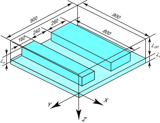
As material for the dielectric bars we propose to use the silicon as most widespread material of electronics which has a transparency window in the wavelength range from 1150 nm to 2500 nm. The sizes of the array elements are chosen to provide the trapped mode resonance of optically non-pumped structure in wavelength 1550 nm, which is the typical wavelength used in telecommunications. In the wavelength 1550 nm, a silicon refractive index is approximately 3.48. Using an extremely thin substrate enables to exclude undesired wave interference. The substrate is assumed to be a synthetic fused silica membrane. Its refractive index is approximately in the wavelength range under consideration Malitson (1965). The substrate thickness is 50 nm. It needs to notice that there are not high non-evanescent diffraction orders in the substrate (an inequality nm is valid).
To study an intensity enhancement of the luminescence of QDs resulted from their hybridization with a dielectric array we propose to use the solutions of plane wave diffraction problem in the cases of the structure with and without optical pump. In proposed method the photoluminescence emission intensity is evaluated as a difference between intensity of dissipation (or emission) defined by expression in the structure without optical pump and with it
| (1) |
where and are intensities of dissipative losses (or emission) in the structure without and with optical pump respectively, and are coefficients of reflection and transmission. It needs to notice that the value will be positive if a dissipation is observed in the structure and negative in the case of a total intensity () of reflected and transmitted waves exceeds the intensity of an incident wave. This fact was taken into account in formula (1) where the photoluminescence intensity has a positive value.
The proposed method was tested for validity on an example of a plasmonic metamaterial combined with QDs which was studied experimentally in Tanaka et al. (2010) (see Appendix). We use the experimental data on a luminescence spectrum presented in Tanaka et al. (2010) to define parameters for a theoretical adequate description of an actual composite material which is QDs dispersed in a host polymer layer. In additional, the comparison of experimental results of this work and our theoretical ones give us an evidence of validity of the proposed theoretical approach to study photoluminescence.
Thus to determine the photoluminescence intensity it is required to solve the plane wave diffraction problem for considered structures. For this aim the mapped pseudospectral time domain method proposed in Gao et al. (2004); Khardikov et al. (2008) is used. For the sake of simplicity the dispersion of dielectrics is not taken into account in this paper. There are two reasons for using such approximation. First, the dispersion of the chosen materials is very weak in the considered wavelength range. Next this, an actual dispersion has no effect on the properties of the trapped-mode resonances.
To take into account a gain in optically pumped QDs the method of additional differential equations Taflove and Hagness (2005) was used with a model of negative frequency-dependent conductivity S. C. Hagness and Taflove (1996). The expression of corresponding time-domain conductivity is chosen in the form to ensure that this value is real and causal
| (2) |
Here is the Heaviside unit step function. The coefficient is proportional to the peak value of the gain set by the pumping level and the resulting population inversion. Such model assumes that the optical gain medium is homogeneously broadened wherein the atoms of the gain medium are indistinguishable and have the same atomic transition frequency, . A natural variation of the QD sizes will cause the broadening of the exciton line of the QDs. Time constant permits to include the relaxation processes in a phenomenological manner (decay rate is ) and shows that any phase coherence introduced into the system of atoms by the action of an electric field will be lost in a time interval once the electric field is turned off.
The Fourier transform of reduces to following frequency-dependent conductivity
| (3) |
where a time dependence of electromagnetic field is chosen in the form . It is clear from (3) that the gain coefficient is governed by a single Lorentzian profile having a width determined by . The resonant frequency, that is the frequency at which the response is maximized, is given by . The peak of the gain curve is and the full-width-at-half-maximum bandwidth is . Using (3) one can obtain a complex propagation constant of a plane wave and see that the wave amplification will be observed only for the case of .
The chosen form of frequency-dependent conductivity may be easily included in the calculation scheme of time domain approaches by using of ADE method. It results in two additional first order differential equations in time in each grid node immersed into the gain medium S. C. Hagness and Taflove (1996).
A good agreement of our theoretical and known experimental results of study luminescence of plasmonic metamaterial combined with QDs (see Appendix) is an evidence of correctness both the model of active QD medium and the proposed approach to study luminescence in a planar resonant metamaterial.
Now let us apply the proposed method to design a silicon resonant metamaterial combined with semiconductor QDs to enhance the photoluminescence intensity with the spectral maximum in wavelength 1550 nm.
For numerical study, a laser medium based on semiconductor QDs was chosen with following parameters: which corresponds to wavelength nm; s; which corresponds to refractive index of non-pumped QD laser medium, and Sm/m corresponding to an emission factor on the analogy of a lossy factor of media. Small value of results in a wide-band QD spectral line and it enables to exclude from consideration the effects caused by displacement of metamaterial dissipation peak and maximum of exciton emission line of QDs. Let us notice that the pump level (parameter ) is in one order less than it was need in the case of plasmonic metamaterials (see Appendix) because of low losses of all-dielectric array.
The geometry parameters of the dielectric bars array immersed in non-pumped QD layer () were chosen to provide a high Q-factor trapped mode resonance of the structure near the wavelength 1550 nm. Parameters of the silicon structure corresponding to this condition are following nm, nm, nm, length of the dielectric bars is 800 nm, widths of bigger and smaller bars are 260 nm and 160 nm respectively, and the distance is 240 nm between two different width bars (see Fig. 1).
To take into account the energy dissipation in dielectric bars, a model of constant conductive medium was used for a description of dielectric in the PSTD method. It means that the dielectric of bars is modeled as medium with both and being some constants. Such approach results in frequency-dependent losses.
III Analysis of luminescence of hybridization of QDs with a low-loss all-dielectric planar metamaterial
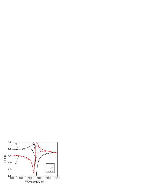
The wavelength dependences of reflection and transmission coefficients magnitudes of the designed structure are shown in Fig. 2. There is a trapped mode resonance near the wavelength 1550 nm which has the typical trough-and-peak Fano spectral profile. As it was shown in Khardikov et al. (2012), this resonance results from the anti-phased excitation of the dielectric bars operated as a half-wavelength dielectric open resonators in this case. Lines 1, 2, and 3 correspond to , Sim/m, and Sim/m or equivalently , , and in the wavelength 1550 nm. Let us notice that in reality the silicon lossy factor is less than in this wavelength.
We estimate the trapped mode resonance Q-factor by using the following formula proposed in Khardikov et al. (2012)
| (4) |
where and are wavelengths of the maximum and minimum of reflection or transmission coefficient of corresponded Fano spectral profile and is an average wavelength of the trapped mode resonance. Using (4) it was obtained following Q-factor values 268, 232 and 83 corresponded to , and . It is interesting that wavelength of maximum and minimum of reflection and transmission coefficients coincide only in the case of non-dissipative structure. Reflection and transmission extremes are shifted relatively to each other when dissipation in dielectric taken into account and then the Q-factor of trapped mode resonances is estimated as the average value . Here and are calculated from wavelength dependences of reflection and transmission coefficients by formula (4). Let us notice that the average trapped mode resonant wavelength nm is observed in all considered cases of dissipative losses.
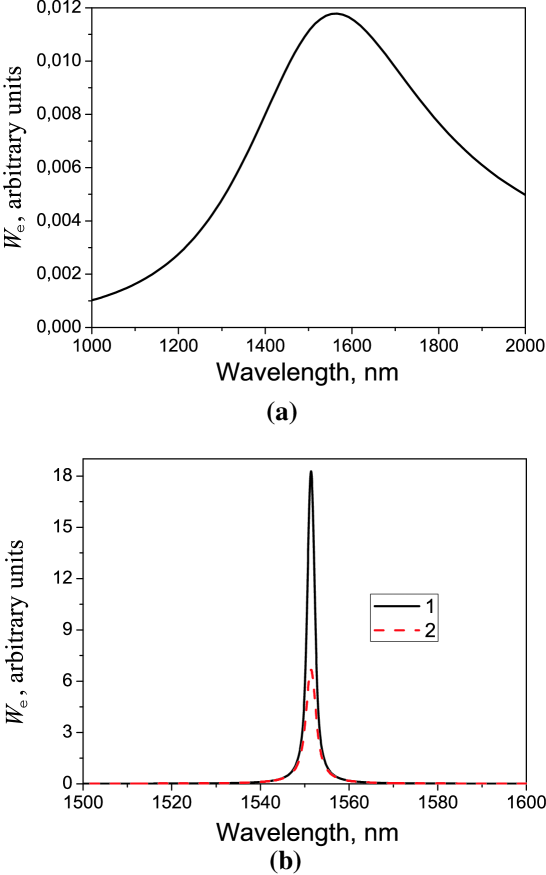
The wavelength dependences of photoluminescence intensity calculated by using (1) are presented in Fig. 3. Fig. 3,a shows the photoluminescence intensity of homogeneous QD layer which thickness is nm placed on 50 nm thick silica membrane i.e. intensity related to layered structure without any array. The wavelength dependencies of photoluminescence of QD hybridization with non-dissipative and low-dissipative () metamaterials are presented in Fig. 3,b. One can see a large enhancement of photoluminescence intensity. For the case of non-dissipative bars the photoluminescence intensity enhances in 1560 times. If the dissipation of silicon estimated as is taken into account, this coefficient of intensity enhancement will be 560. These values are much bigger than known orders of photoluminescence enhancement inherent to plasmonic metamaterials combined with QDs (see Tanaka et al. (2010) and Appendix).
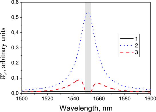
Up to this point we consider photoluminescence in the pumped all-dielectric metamaterial with emission factor () which exceeds essentially in absolute value the lossy factor of metamaterial (). Now let us study the case of pumped lasing medium with the intensity of energy dissipation in the dielectric array () is comparable with the gain of QDs. In Fig. 4 we present wavelength dependences of the photoluminescence intensity of QD-layer placed on silica substrate (line 1), the power dissipation in the array of dielectric bars hybridizing with non-pumped QDs (line 2), and the photoluminescence intensity of optically pumped QDs aggregated with the same array (line 3). In the last case the QD photoluminescence enhancement is observed too (see Fig. 4, line 3). However, in the trapped-mode resonance wavelength, we observe a decrease of emission intensity until complete forbidding photoluminescence (see a grey filled region in Fig.4, where ). Such wavelength dependence of photoluminescence intensity of QDs aggregated with the array is explained by fact that the QD gain results in an increase of field amplitude inside dielectric bars and related increase of energy dissipation in the array. In the case of low energy dissipation (for example the dissipation of silicon array with ) this losses result in a simple decrease of the level of photoluminescence enhancement.
IV Conclusions
We have proposed a simple design of all-dielectric silicon-based planar metamaterial manifested an extremely sharp resonant reflection and transmission in the wavelength of about 1550 nm due to both low dissipative losses and involving trapped mode operating method. Accurate numerical estimations make evidence that the quality factor of the resonance of proposed structure exceeds in tens times the quality factor of known plasmonic structures.
The designed planar metamaterial is envisioned for aggregating with a layer of pumped active medium to achieve an enhancement of luminescence and to produce an all-dielectric analog of the lasing spaser Zheludev et al. (2008).
We have proposed an approach to study luminescence intensity of pumped QDs aggregated with a planar metamaterial. The approach is based on the comparison of results of two diffraction problems solutions. They are the problems of plane electromagnetic wave diffraction by the structure with and without optical pump. The validity of the method has been argued by its application to theoretical reproducing known experimental data on QD luminescence in plasmonic metamaterials Tanaka et al. (2010).
We demonstrate that an essential enhancement (more than 500 times) of luminescence intensity of layer contained pumped QDs may be achieved by using the designed all-dielectric resonant metamaterial. This value exceeds manyfold the known luminescence enhancement by plasmonic planar metamaterials.
V Acknowledgments
This work was supported by the Ukrainian State Foundation for Basic Research, Project F40.2/037.
VI Appendix
Validation of diffraction approach to
study luminescence
For a validation of our approach to choosing parameters described the medium being QDs dispersed in a host polymer and the diffraction approach to study luminescence, let us considered one of the plasmonic metamaterials which were treated experimentally in Tanaka et al. (2010). The sample consists of a gold film patterned periodically by asymmetric split-ring slits and placed on a glass substrate (see Fig. 5). The film thickness is nm. A side size of a square periodic cell of the array is nm. Sizes of the slits of a periodic cell shown in the sketch in Fig. 5 are following: nm, nm, and nm. The slits are filled with a polymer material contained semiconductor QDs and the array is coated by a layer of the same material. The thickness of the layer is nm. In Tanaka et al. (2010) was used lead sulfide (PbS) semiconductor QDs from Evident Technologies with a luminescence peak around 1300 nm and mean core diameter of 4.6 nm. These QDs were dispersed in polymethylmethacrylate (PMMA).
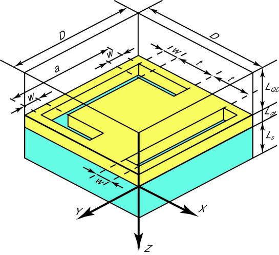
Let us apply the diffraction approach based on the formula (1) to estimate the photoluminescence intensity of QD/PMMA hybridized with this plasmonic metamaterial.
The parameters of gain medium model must be determined before luminescence intensity will be estimated. As it was mentioned above, the following parameters , , and are required to determine a gain medium. Parameters and of QD/PMMA may be determined from the photoluminescence peak frequency and the full-width-at-half-maximum bandwidth of QD/PMMA photoluminescence . We use following values and s. Refractive index of non-pumped QD/PMMA has the value of (see Tanaka et al. (2010)). The value of depends on level of population inversion in QD/PMMA and determines the intensity of photoluminescence. Here we use the value Sim/m to describe an optically pumped QD/PMMA. It is a typical value which was used to describe a gain of semiconductor media for example in S. C. Hagness and Taflove (1996).
We consider the metamaterial aggregated with QD/PMMA placed on a semi-infinite silica substrate (). Such choosing enables us to exclude from the study the interference in the substrate. The model of gold permittivity proposed in Vial and Laroche (2008) was used in our simulation of the plasmonic metamaterial.
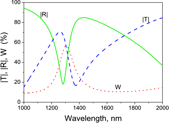
The results of our numerical simulation of wavelength dependences of reflection, transmission, and dissipation coefficients of the metamaterial aggregated with non-pumped QD/PMMA are shown in Fig. 6. These theoretical results may be compared with experimental ones presented in Fig. 1 of Tanaka et al. (2010). One can see a very good agreement between our numerical and measured results. Some difference of levels of reflection, transmission and absorption observed in theoretical and experimental results can be explained by distinctions of the actual structure from the perfect periodic one.
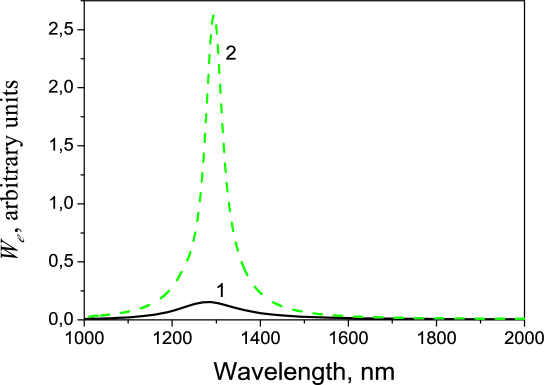
To estimate an enhancement of luminescence intensity due to using metamaterial structure, we compare its value with the luminescence intensity of optically pumped QD/PMMA homogeneous layer placed on the same substrate. The thickness of the layer is chosen the same as a total thickness of the metallic array and its QD/PMMA coating. The wavelength dependences of photoluminescence intensity of QD/PMMA homogeneous layer which being thickness 230 nm (line 1) and metamaterials aggregated with 180 nm-thick QD/PMMA layer (line 2) are shown in Fig. 7. In this case we obtain 17 times enhancement of photoluminescence intensity. This value of luminescence enhancement exceeds only in twice the value obtained experimentally in Tanaka et al. (2010) that is quite good result in modeling of active structures.
Thus, we have argued that the both our model of active QD medium and the diffraction approach to study luminescence intensity result to numerical data being in good correspondence with known measured ones.
References
- Wegener et al. (2008) M. Wegener, J. L. García-Pomar, C. M. Soukoulis, N. Meinzer, M. Ruther, and S. Linden, Optics Express 16, 19785 (2008).
- Fang et al. (2009) A. Fang, T. Koschny, M. Wegener, and C. M. Soukoulis, Physical Review B 79, 241104(R) (2009).
- Sivan et al. (2009) Y. Sivan, S. Xiao, U. K. Chettiar, A. V. Kildishev, and V. M. Shalaev, Optics Express 17, 24060 (2009).
- Bergman and Stockman (2003) D. J. Bergman and M. I. Stockman, Phys. Rev. Lett. 90, 027402 (2003).
- Zheludev et al. (2008) N. I. Zheludev, S. L. Prosvirnin, N. Papasimakis, and V. A. Fedotov, Nature Photonics 2, 351 (2008).
- Campbella and Ziolkowski (2012) S. D. Campbella and R. W. Ziolkowski, Optics Communications 285, 3341 (2012).
- Prosvirnin and Zouhdi (2003) S. Prosvirnin and S. Zouhdi, in Advances in Electromagnetics of Complex Media and Metamaterials, edited by S. Zouhdi and et al. (Kluwer Academic Publishers, Printed in the Netherlands, 2003), pp. 281–290.
- Fedotov et al. (2007) V. A. Fedotov, M. Rose, S. L. Prosvirnin, N. Papasimakis, and N. I. Zheludev, Phys. Rev. Lett. 99, 147401 (2007).
- Zhang et al. (2008) S. Zhang, D. A. Genov, Y. Wang, M. Liu, and X. Zhang, Phys. Rev. Lett. 101, 047401(4) (2008).
- Dong et al. (2010) Z.-G. Dong, H. Liu, M.-X. Xu, T. Li, S.-M. Wang, S.-N. Zhu, and X. Zhang, Opt. Express 18, 18229 (2010).
- Khardikov et al. (2010) V. V. Khardikov, E. O. Iarko, and S. L. Prosvirnin, J. Opt. 12, 045102(11) (2010).
- Tanaka et al. (2010) K. Tanaka, E. Plum, J. Y. Ou, T. Uchino, and N. I. Zheludev, Phys. Rev. Lett. 105, 227403(4) (2010).
- Fano (1961) U. Fano, Phys. Rev. 124, 1866 (1961).
- Khardikov et al. (2012) V. V. Khardikov, E. O. Iarko, and S. L. Prosvirnin, J. Opt. 14, 035103(7) (2012).
- Malitson (1965) I. H. Malitson, JOSA 55, 1205 (1965).
- Gao et al. (2004) X. Gao, M. S. Mirotznik, S. Shi, and D. W. Prather, J. Opt. Soc. Am. A 21, 777 (2004).
- Khardikov et al. (2008) V. V. Khardikov, E. O. Iarko, and S. L. Prosvirnin, Radiophysics and Radioastronomy 13, 146 (2008).
- Taflove and Hagness (2005) A. Taflove and S. C. Hagness, Computational electrodynamics: the finite-difference time-domain method (Artech House, Boston-London, 2005).
- S. C. Hagness and Taflove (1996) R. M. J. S. C. Hagness and A. Taflove, Radio Sci. 31, 931 (1996).
- Vial and Laroche (2008) A. Vial and T. Laroche, Appl. Phys. B 93, 139 (2008).