Thermoelectric efficiency in the space-charge-limited transport regime in semiconductors
Abstract
The thermoelectric efficiency of semiconductors is usually considered in the ohmic electronic transport regime, which is achieved through high doping. Here we consider the opposite regime of low doping where the current-voltage characteristics are nonlinear and dominated by space-charge-limited transport. We show that in this regime, the thermoelectric efficiency can be described by a single figure of merit, in analogy with the ohmic case. Efficiencies for bulk, thin film, and nanowire materials are discussed, and it is proposed that nanowires are the most promising to take advantage of space-charge-limited transport for thermoelectrics.
I
Introduction
Most implementations of thermoelectric devices utilize highly doped semiconductors with linear (ohmic) current-voltage characteristics. In such materials, the thermoelectric efficiency is determined by the figure of merit where is the Seebeck coefficient, the electrical conductivity, the temperature, and the thermal conductivity. The factor has governed much of the research in developing approaches to improve thermoelectric efficiency; however, the intimate relationship between transport quantities places constraints on the possible paths towards efficiency improvements. Thus, new approaches where the thermoelectric efficiency does not depend on would open new routes for scientific exploration.
An example of such an approach is thermionic cooling and power generation, which was originally considered for injection into vacuummahan , and then into semiconductorsshakouri . These thermionic devices are often considered different from thermoelectric devices due to the presence of an injection barrier and because the channel length is shorter than the electronic mean-free path, giving ballistic electron transportnolas ; ulrich ; mahan2 . However, as the channel length increases beyond the mean-free path, thermionic devices become equivalent to thermoelectric devicesmahan3 ; zeng , which has led to new proposals to engineer multilayer semiconductor materialsodwyer .
In this manuscript, we explore an alternative approach that does not rely on ohmic transport or thermionic emission, but instead exploits space-charge-limited (SCL) electronic transport in a semiconductor. We derive an expression for thermoelectric efficiency in this regime, and show that it depends on a new dimensionless figure of merit that replaces . Furthermore, we apply the theory to bulk, thin film, and nanowire materials, and conclude that nanowires are the most promising to harness SCL transport for thermoelectrics.

The term ”space-charge-limited” originated from the consideration of charge injection into a region where electronic transport is ballistic. In that case, space-charge effects are detrimental because they create an additional barrier for injection compared with the reference space-charge-free systemlampert . This situation is relevant to thermionic devices where space-charge effects have been shown to reduce efficiencymahan . The issue of space-charge is different if one considers semiconductor-based thermoelectric devices. There, the reference system is a highly-doped semiconductor with two ohmic contacts. In that case, space-charge effects are minimal because the high doping immediately screens the injected charge. However, if the doping in the semiconductor is lowered, space charge effects become dominant, and the current becomes larger than the ohmic current because electronic transport is no longer determined by the free-carrier relaxation time, but by the shorter carrier transit timelampert . This situation, which has been observed experimentally in a broad range of materials, is the one that we consider in this manuscript.
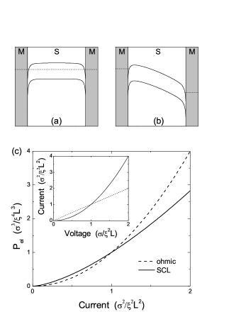
Figure 1 shows the system under consideration: a low-doped semiconductor between two ohmic contacts. Band diagrams are shown in Figs 1a,b for the case relevant to electron injection: the metal Fermi level contacts the semiconductor in the conduction band creating a large density of carriers in the near-interface region. Band-bending away from the metal/semiconductor interface creates a barrier for electron injection at zero bias. Under bias, a maximum in the potential is created near the injecting electrode, defining the so-called ”virtual cathode”rose . Modeling has demonstrated that in the presence of this virtual cathode, SCL transport dominates as soon as the applied bias exceeds a few grinberg1 . This leads to a current-voltage relationship as discussed further below. This relationship differs from the exponential characteristics usually considered for thermionic systemsmahan ; the transitions between the thermionic and SCL regimes and the role of Schottky barriers has been studied in detaildavids ; chandra , demonstrating that SCL dominates even when small Schottky barriers are present.
II Thermoelectric efficiency
To be specific, we consider the thermoelectric power generation efficiency of the system of Fig. 1, but the approach should apply to cooling as well. The efficiency of a thermoelectric material for power generation is given bysnyder
| (1) |
where is the thermoelectric power generated, is the electrical power dissipated, and is the thermal power supplied. Here and are the cold and hot side temperatures and is the local potential.
Usually, one considers a highly doped semiconductor of length between ohmic contacts. For a bias voltage , there is a linear drop of the potential along the channel due to the free-carrier screening; this leads to , giving and the dependence of the efficiency on snyder . For SCL transport, the transport equations need to be solved self-consistently with the Poisson equation due to the unscreened space-chargegrinberg ; in the simplest model with diffusive electronic transportgrinberg , this gives an electrostatic potential that depends on position as
| (2) |
This nonlinear spatial dependence of the potential leads to the current-voltage relationship grinberg
| (3) |
Thus, in the SCL regime, the current is no longer linear in , but is quadratic instead. The proportionality constant depends on the dimensionality of the material, and to some extent on the shape of the electrodes, as will be discussed further below.
The quadratic form of the behavior implies that ; the interest in this transport regime for thermoelectrics is illustrated in Fig. 1c, where for the ohmic and SCL regimes are compared. There, in the SCL regime is below that of the ohmic regime at sufficiently high voltage, suggesting a potentially new regime of operation for thermoelectrics. (The cross-over between ohmic and SCL transport occurs at , as shown in the Fig. 1c inset. This sets a condition for when ohmic contributions should be negligible compared to SCL transport.)
To derive the thermoelectric efficiency in this regime, we utilize the approach described in Ref. snyder . From the above equations we obtain for the local efficiency
| (4) |
where we used , and where the prefactor indicates that the efficiency is limited by the Carnot efficiency. The temperature depends on position through the heat equationleonard
| (5) |
The first term on the right hand side is the usual Thomson effect, while the second term is the local Joule heating in the material . This equation applies for SCL transport because both the electronic and phononic transport are diffusive, and thus both the electronic and phononic thermal conductivities are well defined (this has been demonstrated for SCL transport in nanowireskatzenmeyer ).
The total efficiency of a segment is obtained fromharman
| (6) |
Noticing that and assuming that the coefficients are independent of temperature and position we arrive at
| (7) |
Thus, the efficiency depends only on quantities evaluated at the cold and hot sidessnyder . To obtain these quantities we integrate the heat equation to get
| (8) |
which leads to
| (9) |
where
| (10) |
and
| (11) |
The variable is a dimensionless quantity equal to the ratio between the generated voltage and the maximum thermoelectric voltage that can be developed across the material. is a dimensionless parameter that replaces the factor from conventional ohmic materials. (Note that the average temperature does not directly appear in . However, we use the notation as a reminder that, as a first approximation, the quantities that enter should be evaluated at the average temperature across the material.)

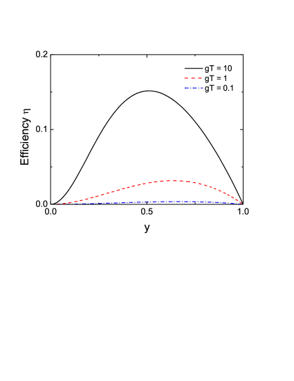
Figure 2 shows the dependence of the efficiency on from Eq. , indicating that positive efficiency is achieved in the range , with a maximum attained at an intermediate value. This behavior is similar to that obtained for conventional ohmic lossessnyder , but with a different functional dependence.
The maximum efficiency is obtained by maximizing with respect to to obtain
| (12) |
This equation provides the optimal that maximizes the efficiency:
| (13) |
where and . At this optimal the efficiency is given by
| (14) |
Thus, the efficiency only depends on and , much like ohmic materials where the dependence is on and .
Figure 3a shows the calculated efficiency as a function of for , indicating low efficiency at small and efficiencies approaching the Carnot efficiency at large . The two limiting cases of small and large can be obtained as
| (15) |
thus providing simple analytical expressions for these two regimes. The small expression provides a good estimate of the full curve up to about 1% efficiency, while the large approximation is valid for .

The inset in Fig. 3a shows the efficiency for a traditional ohmic material as a function of for , where gives about 10% efficiency. Since this is the current state-of-the-art in thermoelectric materials, we can use it as a comparison with the SCL regime; in that case one would need to achieve the same efficiency at this given . However, the efficiency depends significantly on , as shown in Fig. 3b for values of as high as 10. The curve for is well approximated by the small limit of Eq. , indicating a quadratic dependence on .
The full expression for depends on the parameter , which in turn depends on the dimensionality of the material under consideration; for bulkgrinberg , thin filmgrinberg , and nanowiretalin materials, it is given by
| (16) |
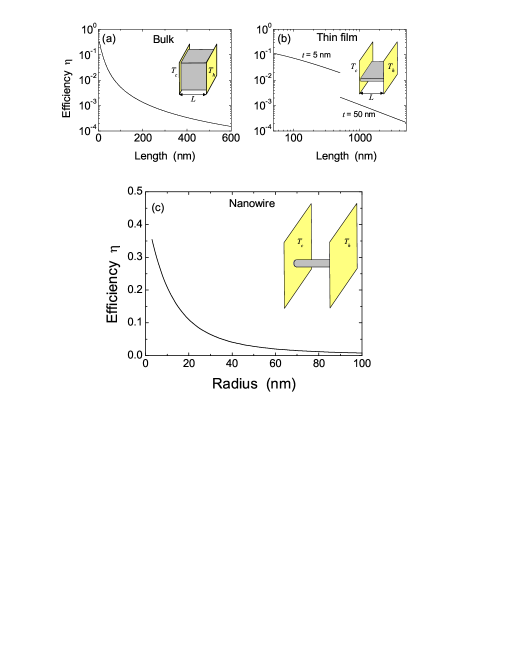
where is the permittivity, is the mobility, and is a numerical constant that depends on the shape of the electrodes, equal to 1 for planar contactsgrinberg . is the thickness of the thin film, while is the nanowire radius (see Fig. 4 for illustrations of the different geometries.) The expressions for the thin film and nanowire cases are applicable when and ; for larger values of and , crosses over to the bulk expressiontalin .
The factor also depends on the material parameters , , , and . Like traditional ohmic materials, high requires large , low and large ; but it also needs large , a criterion not usually required for high . This arises because large serves to screen the injected charge, and reduces the repulsive Coulomb interaction that opposes charge injection. This is beneficial because dielectric screening maintains the SCL transport regime, in contrast to free-carrier screening that would make the current ohmic.
Two advantages of the SCL regime are that the maximum values of and can be exploited. Indeed, ohmic materials are usually operated at high doping where both and are reduced from their maximum values. But at low doping attains a maximum at a valuegoldsmid while saturates to its intrinsic value . We can thus write the maximum value of as
| (17) |
where is a geometry-dependent factor that can be obtained from Eq. . We note that the factor depends linearly on , just like an ohmic material where ; however, the difference is that the mobility in is the high-doping mobility, which is smaller than .
III Practical estimates
To evaluate the practicality of the SCL approach for thermoelectric power generation, we apply the theory to the bulk, thin film, and nanowire geometries for K and = 300K. We consider GaAs at low doping as an example material since SCL has been observed in this materialallen , and because material properties are readily availableblakemore : at K and low doping, 1.35 eV, , cm, and 30 W/mK. Figure 4a shows the calculated efficiency for a bulk device as a function of the channel length . The efficiency is low unless is very small. The case of thin films (Fig. 4b) is slightly more promising with larger efficiencies at longer lengths, but this requires small film thicknesses. Also note that the large over the small lengths where reasonable efficiency is observed in Fig. 4a and 4b would lead to very large heat fluxes that further limit the usefulness of these geometries. Thus, for the bulk or thin film geometries to be useful, a much larger is needed so they can operate at longer lengths, and this would require other or new materials with better properties for SCL thermoelectrics.

The situation is significantly more favorable if one considers nanowires, as shown in Fig. 4c. In that case, SCL currents are enhanced due to the scaling ; in fact, becomes independent of length, and scales as , with being naturally small for nanowires. This leads to a large efficiency which exceeds the 10% value for nanowires less than 20nm in radius. This efficiency could be even larger if other effects predicted and measured for nanowires were included; for example, from Eq. , depends sensitively on the bandgap, which increases with decreasing diameter. Similarly, the thermal conductivity is reduced with decreasing nanowire diameter, which could also make larger. It should be noted that the electrical currents needed to achieve the efficiency plotted in Fig. 4c are less than a per nanowire and require voltages on the order of a volt, which is easily achieved without damaging the nanowires or the contactstalin .
IV Conclusion
In summary, we considered the efficiency of thermoelectric materials in the space-charge-limited regime and found that it depends on a single dimensionless parameter , in analogy with conventional ohmic materials. When applied to bulk, thin film and nanowire geometries, we find that nanowires are the most promising to harness SCL transport. This work provides a new path for improving the performance of thermoelectric materials, and suggests the exploration of new thermoelectric materials with properties conducive to SCL transport.
V Acknowledgement
Discussions with Peter Sharma and Doug Medlin are gratefully acknowledged. This project is supported by the Laboratory Directed Research and Development program at Sandia National Laboratories, a multiprogram laboratory managed and operated by Sandia Corporation, a wholly owned subsidiary of Lockheed Martin Corporation, for the United States Department of Energy’s National Nuclear Security Administration under Contract DE-AC04-94AL85000.
∗email:fleonar@sandia.gov
References
- (1) G. Mahan, J. Appl. Phys. 76, 4362 (1994).
- (2) A. Shakouri, Annu. Rev. Mater. Res. 41, 399 (2011).
- (3) G. S. Nolas, J. Sharp, and H. J. Goldsmid, Thermoelectrics Basic Principles and New Materials Developments (Springer, Berlin, 2001).
- (4) M. D. Ulrich, P. A. Barnes, and C. B. Vining, J. Appl. Phys. 90, 1625 (2001).
- (5) G. D. Mahan, J. O. Sofo, and M. Bartkowiak, J. Appl. Phys. 83, 4683 (1998).
- (6) G. D. Mahan, J. Appl. Phys. 87, 7326 (2000).
- (7) T. Zeng and G. Xhen, J. Appl. Phys. 92, 3152 (2002).
- (8) M. F. O’Dwyer, T. E. Humphrey, R. A. Lewis, and C. Zhang, J. Phys. D: Appl. Phys. 39, 4153 (2006).
- (9) M. A. Lampert and P. Mark, Charge Injection in Solids (Academic Press, New York, 1970).
- (10) A. Rose, Phys. Rev. 97, 1538 (1955).
- (11) A. A. Grinberg and S. Luryi, J. Appl. Phys. 61, 1181 (1987).
- (12) P. S. Davids, I. H. Campbell, and D. L. Smith, J. Appl. Phys. 82, 6319 (1997).
- (13) W. Chandra, L. K. Ang, and W. S. Koh, J. Phys. D: Appl. Phys. 42, 055504 (2009).
- (14) G. J. Snyder and T. S. Ursell, Phys. Rev. Lett. 91, 148301 (2003).
- (15) A. A. Grinberg, S. Luryi, M. R. Pinto, and N. L. Schryer, IEEE Trans. Electron Devices 36, 1162 (1989).
- (16) The heat equation for nanowires is discussed in F. Léonard, Appl. Phys. Lett. 98, 103101 (2011).
- (17) A. M. Katzenmeyer et al, IEEE Trans. Nanotech. 10, 92 (2011).
- (18) T. C. Harman and J. M. Honig, Thermoelectric and Thermomagnetic Effects and Applications (McGraw-Hill, New York, 1967).
- (19) A. A. Talin, F. Léonard, B. S. Swartzentruber, X. Wang, and S. D. Hersee, Phys. Rev. Lett. 101, 076802 (2008).
- (20) H. J. Goldsmid and J. W. Sharp, J. Electron. Mater. 28, 869 (1999).
- (21) J. W. Allen and R. J. Cherry, Nature 189, 297 (1961).
- (22) J. S. Blakemore, J. Appl. Phys. 53, R123 (1982).