Tunable Kondo physics in a carbon nanotube double quantum dot
Abstract
We investigate a tunable two-impurity Kondo system in a strongly correlated carbon nanotube double quantum dot, accessing the full range of charge regimes. In the regime where both dots contain an unpaired electron, the system approaches the two-impurity Kondo model. At zero magnetic field the interdot coupling disrupts the Kondo physics and a local singlet state arises, but we are able to tune the crossover to a Kondo screened phase by application of a magnetic field. All results show good agreement with a numerical renormalization group study of the device.
pacs:
73.63.Kv, 73.63.Fg, 73.23.Hk, 72.15.QmA quantum dot coupled to two leads can be considered as an experimental realization of the single-impurity Anderson model Anderson . When the dot contains a single unpaired electron, the Anderson model accurately describes how, below a characteristic temperature , correlated electron tunnelling between the quantum dot and the leads results in coherent screening of the electron spin Goldhaber ; Cronenwett ; Nygard . The combined system of electrons on the quantum dot and leads forms a spin singlet, a phenomenon known as the Kondo effect Hewson . Likewise, two tunnel-coupled quantum dots should amount to an experimental realization of the two-impurity Anderson model Alexander . Here the physics is much richer, particularly in the regime where each dot contains an unpaired electron. In this case, a competition now arises between the tendency of the conduction electrons on the leads to screen the spins on the quantum dots, and the antiferromagnetic exchange coupling between the two localized spins. The former favors formation of a Kondo singlet between each lead and the dot to which it is coupled, while the latter favors a local singlet state. The resulting groundstate of the system depends sensitively on the relative strength of the interactions, an understanding of which is important and believed to underlie the electronic properties of a wide range of strongly correlated materials, including spin glasses and heavy fermion compounds Hewson .
The essence of this competition is captured by the two-impurity Kondo model Jaya ; Jones1 ; Afflec92 ; Afflec95 , which describes the low-energy physics of the two-impurity Anderson model in the absence of charge transfer between the leads, and famously contains a quantum phase transition at the boundary of the local and Kondo singlet phases where . While this has attracted considerable experimental attention Jeong ; Craig ; Bork , observation of the transition has remained elusive. This is perhaps unsurprising as charge transfer between the leads, absent in the two-impurity Kondo model, is necessarily present in experiment if a conductance is measured. As is well known theoretically, this transforms the quantum phase transition into a crossover, such that the ground state of the system is always a Fermi liquid Afflec95 ; Jayatilaka ; although remnants of the transition are evident in a strong enhancement of the zero-bias conductance in the vicinity of Georges ; saka:2000 ; sela:2009 .
An understanding of the transport properties of a realistic two-impurity system, such as a double quantum dot (DQD), thus requires that charge transfer between the leads is taken into account. This is achieved in the present work, where we present a study of a tunable carbon nanotube DQD in the strongly correlated regime, and use a numerical renormalization group (NRG) study of the two-impurity Anderson model to describe the device. We show that in the charge regime where both dots have an unpaired electron, the ground state of the device is a local singlet phase with suppressed Kondo correlations. The ability to tune the exchange coupling and the Kondo scales allows one, in principle, to crossover from the local singlet to the Kondo screened phase. In our device the onset of charge fluctuations prevents the crossover being seen cleanly at zero magnetic field. We have, however, been able to observe it at finite magnetic field, consistent with recent theoretical predictions Jayatilaka .
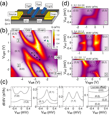
The device we consider is a single-walled carbon nanotube on a degenerately doped Si/SiO2 substrate contacted by Au contacts, see Fig. 1(a) epaps . A central gate is used to introduce a tunable tunnel barrier, separating the nanotube into two quantum dots, which can be individually addressed by two additional side gates. The stability diagram of the device is shown in Fig. 1(b). The effective electron number of each charge regime is indicated by the ordered pairs . The large-small-large alternation in the stability diagram reflects the two-fold spin degeneracy of the device, and allows us to establish unambiguously the parity of the electron number (even or odd). The orbital degeneracy of the nanotubes is broken, most likely as a result of mixing Liang ; Buitelaar1 .
From an analysis of the stability diagram we are able to extract the on-site charging energies meV for both dots, the electrostatic coupling energy meV and the interdot tunnel coupling meV. The widths of the Coulomb blockade peaks in the stability diagram allow an estimate of the coupling between the dots and the leads. In the non-interacting limit the full-width at half maximum is equal to , but the peaks are broadened by a further factor of by many-body scattering processes Block . Bearing this in mind, we obtain meV and meV for the right and left dot respectively. For these coupling strengths , so we might expect co-tunneling processes, and thus the Kondo effect, to be experimentally observable. To investigate the presence of Kondo correlations, we measured the differential conductance in all charge regimes, see Fig. 1(c) and 1(d). When both dots contain an even number of electrons, the Kondo effect is inoperative and conductance is suppressed and featureless around source-drain bias . On the other hand, when one of the quantum dots contains an odd number of electrons, we observe a pronounced zero-bias conductance peak. The evolution of the differential conductance as electrons are added to the right dot, keeping the effective electron number of the left dot fixed at , is shown in the top-most panel of Fig. 1(d). The characteristic appearance of a zero-bias peak when the electron number is odd is a clear indication of Kondo physics in the (0,1), (1,0), (1,2) and (2,1) charge regimes Goldhaber ; Cronenwett ; Nygard , the spin of the singly-occupied dot being effectively Kondo screened by the lead to which it is coupled.
The behavior, however, is markedly different in the center of the (1,1) charge regime where the electron number is odd for both dots. As shown in Fig. 1(c), the zero-bias conductance is suppressed and a double peak structure arises at finite bias Jeong ; Craig . The behavior we observe is characteristic of a strongly correlated DQD when where denote the Kondo scales for the left and right dots respectively. These energy scales are readily estimated using the parameters obtained above. In the center of the (1,1) charge regime the exchange coupling , which yields meV. The Kondo scales can be estimated roughly using the Haldane expression Haldane
| (1) |
where () is the level energy of dot relative to the zero-bias Fermi level of the leads. This yields meV and meV in the middle of the (1,1) charge regime, such that .
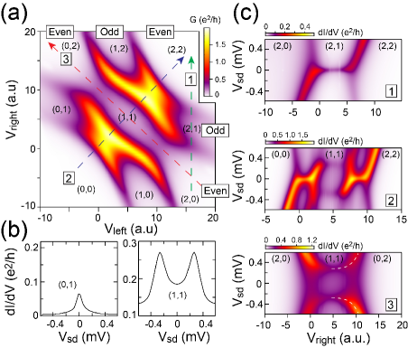
The above interpretation of the measurements is strengthened by an NRG study of our double quantum dot. The calculated stability diagram using the experimental parameters, see Fig. 2(a), reproduces all key features of the experiment and allows for a comparison between experiment and theory (for further details see supplementary material epaps ). Finite-bias conductances, NRG calculation of which is inevitably approximate (see epaps ), are also in good agreement. In particular the double peak structure in the (1,1) charge regime is reproduced in the calculations, see Fig. 2(b). It can be understood physically as a non-equilibrium Kondo effect Paaske . While the formation of a local singlet state suppresses Kondo correlations at zero-bias, interlead spin-flip tunneling becomes possible and Kondo correlations are partially restored when is comparable to the exchange energy separating the atomic-limit singlet ground state from its triplet excited states. As demonstrated below, a unique feature of double quantum dots is that and are all tunable by varying the dot level energies.
We discuss first the behavior along diagonal 2 in Fig. 1(b), for which the differential conductance is shown in Fig. 1(d), middle panel. Along this diagonal, the dot level energies are decreased while their difference (or detuning) remains zero. This allows us to tune the Kondo scales of the two quantum dots, as these strongly depend on the dot level energies, see Eq.(1). In the center of the (1,1) charge regime, the Kondo scales for both dots are at a minimum. Moving away from the center, the Kondo scales thus increase. However, before we can access the Kondo screened phase we reach the edge of the (1,1) charge regime, moving into a mixed-valence regime. Here charge fluctuations are significant, and a two-impurity Kondo model description is no longer valid. The inability to access the Kondo screened phase this way can be understood given that for our device , so to observe the crossover requires , which occurs only when , i.e. in the mixed-valence regime. A lower is therefore required in order to observe the crossover cleanly in this way. While we were able to control the tunnel coupling experimentally (see epaps ), sufficiently small values of it were not reached here.
We now focus on the behavior along diagonal 3 in Fig. 1(b) for which the differential conductance is shown in Fig. 1(d), bottom panel. Along this diagonal the detuning () is increased while is constant. As indicated by the dashed white line in Fig. 1(d) the peaks observed in the differential conductance move further apart as the magnitude of the detuning is increased and the conductance becomes highly asymmetric in bias. This increase in peak splitting is due to becoming larger with positive detuning as the (1,1) singlet state becomes closer in energy to the (0,2) singlet J . The ability to tune the exchange energy by varying the detuning is essential in spin-based quantum information processing schemes using quantum dots Chorley . Importantly, the present data shows that this tunability can also be used as a probe of Kondo physics.
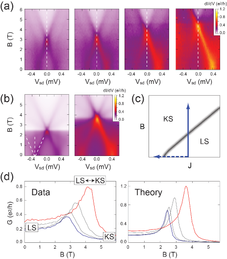
The consequences of varying the exchange are investigated further in Fig. 3 by application of a magnetic field () perpendicular to the nanotube axis, for various values of the detuning along diagonal 3 in the regime. At finite the observed zero-field peaks split into three components, Fig. 3(a) (of which the innermost peaks are most easily resolved, see Figs. 3(a,b)), consistent with a local singlet ground state and triplet excited state, separated by at . As is increased, the energy difference () between the singlet () and the lowest-energy triplet state, , decreases. At a field these states are near-degenerate. A strong zero-bias conductance peak is then observed, due to Kondo screening of the - pseudospin system PustKikoin ; PustGlazman ; Florens , here by two channels. [In our tunnel-coupled double QD both the and states arise from the charge configuration, in contrast to - crossings observed Nygard ; Paaske ; Zumbuhl ; Roch in single QDs with two ‘active’ levels, where the relevant singlet is a configuration with the lower dot level doubly occupied faraway , and consequent Kondo screening arises by a single effective channel PustKikoin .]
From the perspective of the two-impurity Anderson model, and its experimental realization in our device, this conductance peak is the signature of the finite-field crossover from a local singlet (LS) phase for , to a polarized Kondo screened (KS) phase for ; and amounts to a finite- continuation of the zero-field conductance peak at Jayatilaka ; Georges ; saka:2000 ; sela:2009 . For a L-R symmetric two-impurity Kondo model, it was recently shown Jayatilaka that the well known zero-field quantum phase transition between LS and KS phases, occurring at , extends into the -plane (Fig. 3(c)). The transition could thus be driven either by tuning through at zero-field, or by tuning through a critical at fixed . With interlead charge transfer and L-R asymmetry, both of which occur in our device, the transition line is of course broadened into a line of crossovers (Fig. 3(c)) with associated conductance peaks. For in particular, where the system at zero-field is deep in the LS phase, (and the Kondo screened phase for is naturally spin polarized, asymptotically approaching the free state). This behavior is observed clearly in Fig. 3(d). In the center of the (1,1) regime, meV (as estimated above) yields T, in very good agreement with the measured conductance peak in Fig. 3(d) epaps . As detuning increases, becomes larger as noted above, and is correspondingly seen to increase. The evolution of conductance as a function of magnetic field is in good agreement with the NRG calculations as shown in Fig. 3(b,d). The calculations also confirm (not shown) that the asymmetry in observed (Fig. 3(a)) in the differential conductance with increasing detuning, results from the asymmetry . For symmetric coupling strengths, or precisely at the center of the (1,1) charge regime where the system is electron-hole symmetric [e.g. the leftmost plot in Fig. 3(a)], no asymmetry is observed in the differential conductance.
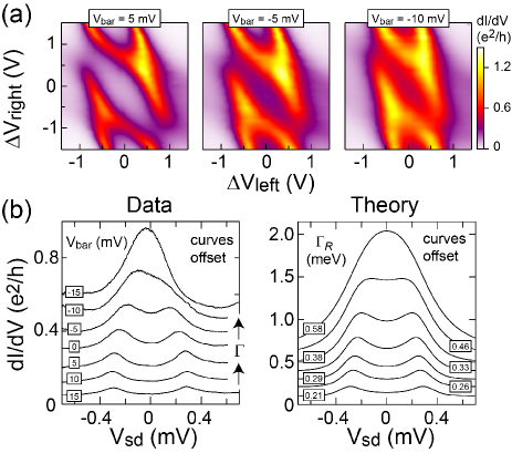
Finally, we show that by varying (see Fig. 1(a)) we can directly tune the coupling strengths between the quantum dots and their leads coupling . This is illustrated in Fig. 4(a) which shows that for decreasing , the conductance at the center of the (1,1) charge regime strongly increases. At the same time, the double peak structure, clearly observed for higher values of , gradually merges into one broad peak. This behavior can be understood as an increase in the coupling strengths , as illustrated by NRG calculations, see Fig. 4(b), and consistent with the increase in widths of the Coulomb blockade peaks in the stability diagrams. On increasing , and hence decreasing , the device becomes less strongly correlated and charge fluctuations consequently more significant, thereby eroding and ultimately destroying the double peak structure that is characteristic of the strongly correlated regime of the DQD.
In conclusion, we have investigated a tunable two-impurity Kondo system in a strongly correlated carbon nanotube DQD, in which the full range of charge regimes is accessible, and which amounts to a clear experimental realization of a two-impurity Anderson model. In the (1,1) regime, we have shown that the exchange and Kondo energy scales can be varied by tuning the dot energy levels or by varying the dot-lead tunnel couplings, providing the possibility of observing the crossover between local singlet and Kondo screened phases. While charge fluctuations in this device prevented observation of the crossover at zero field, we were able to observe it at finite field, indicated by enhanced zero-bias conductance. The work is readily extended to carbon nanotube DQDs coupled to superconducting Buitelaar2 or ferromagnetic Hauptmann leads. This allows experimental access to rich phase behavior controlled by the interplay between Kondo, exchange, and superconducting correlations, and further highlights the potential of carbon nanotube quantum dots to investigate correlated electron physics.
Acknowledgments.– We thank David Cobden and Jiang Wei for the carbon nanotube growth. M.R.B. is supported by the Royal Society, and D.E.L. acknowledges support from EPSRC through EP/I032487/1.
References
- (1) P.W. Anderson, Phys. Rev. 124, 41 (1961).
- (2) D. Goldhaber-Gordon, H. Shtrikman, D. Mahalu, D. Abusch-Magder, U. Meirav, and M.A. Kastner, Nature (London) 391, 156 (1998).
- (3) S.M. Cronenwett, T.H. Oosterkamp, and L.P. Kouwenhoven, Science 281, 540 (1998).
- (4) J. Nygård, D.H. Cobden, and P.E. Lindelof, Nature (London) 408, 342 (2000).
- (5) A.C. Hewson, The Kondo Problem to Heavy Fermions (Cambridge University Press, Cambridge, 1993).
- (6) S. Alexander and P. W. Anderson, Phys. Rev. 133, A1594 (1964); P. Gottlieb and H. Suhl, ibid. 134, A1586 (1964).
- (7) C. Jayaprakash, H.R. Krishnamurthy, and J.W. Wilkins, Phys. Rev. Lett. 47, 737 (1981).
- (8) B.A. Jones and C.M. Varma, Phys. Rev. Lett. 58, 843 (1987); Phys. Rev. B 40, 324 (1989).
- (9) I. Affleck and A. W. W. Ludwig, Phys. Rev. Lett. 68, 1046 (1992).
- (10) I. Affleck, A. W. W. Ludwig, and B.A. Jones, Phys. Rev. B 52, 9528 (1995).
- (11) H. Jeong, A.M. Chang, and M.R. Melloch, Science 293, 2221 (2001).
- (12) N.G. Craig, J.M. Taylor, E.A. Lester, C.M. Marcus, M.P. Hanson, and A.C. Gossard, Science 304, 565 (2004).
- (13) J. Bork et. al., Nature Phys. 7, 901 (2011).
- (14) F. W. Jayatilaka, M. R. Galpin and D. E. Logan, Phys. Rev. B 84, 115111 (2011).
- (15) A. Georges and Y. Meir, Phys. Rev. Lett. 82, 3508 (1999).
- (16) W. Izumida and O. Sakai, Phys. Rev. B, 62, 10260 (2000).
- (17) E. Sela and I. Affleck, Phys. Rev. Lett. 102, 047201 (2009).
- (18) See supplementary material at (url to be inserted) for details of device fabrication, and additional experimental data on the dependence of conductance on applied magnetic field, temperature and interdot and dot-lead tunnel coupling; together with details of the Hamiltonian used in the NRG calculations, and how the conductance is calculated.
- (19) W.J. Liang, M. Bockrath, and H. Park, Phys. Rev. Lett. 88, 126801 (2002).
- (20) M.R. Buitelaar, A. Bachtold, T. Nussbaumer, M. Iqbal and C. Schönenberger, Phys. Rev. Lett. 88, 156801 (2002).
- (21) F. B. Anders, D. E. Logan, M. R. Galpin and G. Finkelstein, Phys. Rev. Lett. 100, 086809 (2008); N. E. Bickers, Rev. Mod. Phys. 59, 845 (1987).
- (22) F.D.M. Haldane, Phys. Rev. Lett. 40, 416 (1978).
- (23) J. Paaske, A. Rosch, P. Wölfle, N. Mason, C.M. Marcus, and J. Nygård, Nature Phys. 2, 460 (2006).
- (24) In the (1,1) regime, , and thus increases with detuning .
- (25) S.J. Chorley et. al., Phys. Rev. Lett. 106, 206801 (2011).
- (26) M. Pustilnik, Y. Avishai and K. Kikoin, Phys. Rev. Lett. 84, 1756 (2000).
- (27) M. Pustilnik and L. I. Glazman, Phys. Rev. Lett. 85, 2993 (2000); Phys. Rev. B 64, 045328 (2001).
- (28) S. Florens et. al., J. Phys: Condens. Matt. 23, 243202 (2011).
- (29) D. M.Zumbühl, C. M. Marcus, M. P. Hanson and A. C. Gossard, Phys. Rev. Lett. 93, 256801 (2004).
- (30) N. Roch, S. Florens, V. Bouchiat, W. Wernsdorfer and F. Balestro, Nature 453, 633 (2008).
- (31) In our case by contrast, states such as or are higher in energy than the states close to the center of the charge regime, and thus irrelevant.
- (32) In general, varying the barrier gate voltage affects both the tunnel coupling and the coupling to the leads. For the charge configuration here the main effect is on the lead couplings.
- (33) M.R. Buitelaar, T. Nussbaumer, and C. Schönenberger, Phys. Rev. Lett. 89, 256801 (2002).
- (34) J.R. Hauptmann, J. Paaske, and P.E. Lindelof, Nature Phys. 4, 373 (2008).
Tunable Kondo physics in a carbon nanotube double quantum dot:
Supplementary Material
S. J. Chorley,1 M. R. Galpin,2 F. W. Jayatilaka,2 C.
G. Smith,1 D. E. Logan2 and M. R. Buitelaar1
1Cavendish Laboratory, University of
Cambridge, Cambridge CB3 0HE, United Kingdom
2Department of Chemistry, Physical and Theoretical Chemistry
Laboratory,
Oxford University, South Parks Road, Oxford OX1 3QZ,
United Kingdom
The following appendices comprise the supplementary material to Ref. Spaper, . We provide the following: (i) details of device fabrication; (ii) additional experimental data on the dependence of the double quantum dot (DQD) conductance on the applied magnetic field, temperature and interdot and dot-lead tunnel coupling; and (iii) details of the model Hamiltonian used in the numerical renormalization group (NRG) calculations, and how the conductance is calculated from the NRG.
I Device fabrication
Carbon nanotubes were synthesized by chemical vapor deposition using a procedure similar to Ref. SKong, . To form the catalyst particles, g/cm3 Fe(NO3).9H2O (Sigma-Aldrich) was sonicated in isopropanol. The bare Si/SiO2 substrate (300 nm thermal oxide) was dipped into the solution immediately after sonication and dried by air blowing. It was then heated to 900 ∘C in a 1" tube furnace under a hydrogen gas flow of 400 sccm, during which the iron nitrate was reduced to iron particles. Once at this temperature, 500 sccm of methane (containing natural isotope ratios) was added to the flow for 8 minutes. After the methane flow was stopped, the substrate was cooled under the same 400 sccm hydrogen flow. Alignment marks were defined by electron-beam lithography, and scanning electron microscopy and atomic force microscopy were used to locate the nanotubes in relation to these. Further steps of electron-beam lithography and evaporation contact the nanotubes with 20 nm thick, 300 nm wide gold ohmic contacts, separated by 700 nm, which also form the outer barriers of the quantum dots. The final electron-beam lithography layer writes the 100 nm wide and 100 nm spaced gates, which are made from two 1.2 nm layers of aluminum, oxidized in air and capped with a further 20 nm of titanium and 6 nm of gold. The source lead is grounded by the virtual earth of a current to voltage preamplifier, and the drain has a small variable dc bias applied. The chip is mounted on the cold finger of a 60 mK dilution refrigerator and connected to the measurement apparatus with filtered low-frequency lines.
II Magnetic field and temperature behavior
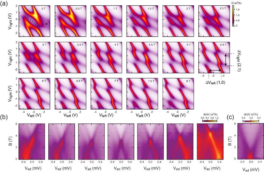
Figure S1(a) shows the evolution of the double quantum dot stability diagram with magnetic field in steps of 0.5 T. We first focus on the widths of the hexagons (1,0) and (2,1). In the atomic limit (no coupling between the dots and their leads) the width of the hexagon increases proportional to for a magnetic field applied perpendicularly to the nanotube axis, where we assume for nanotubes. In practice our device has a relatively strong coupling between the dot and leads, and a linear relation between the width of the hexagons and is a good approximation only in the limit of large magnetic field. Bearing this in mind, we obtain the coupling strengths (or lever arms) between the gate electrodes and the quantum dots, and extract charging energies meV for both quantum dots and an electrostatic coupling energy meV.
The differential conductance as a function of magnetic field is shown in Figs. S1(b) and (c) - which are an extension of Fig. 3 in the main text - for different positions in the stability diagram. Fig. S1(b) shows the differential conductance as a function of magnetic field for seven positions in the (1,1) charge region as indicated by the circles in the diagram in panel (a). Fig. S1(c) shows the differential conductance as a function of magnetic field in the center of the (2,1) charge region as indicated by the square in the diagram in panel (a). The maximum conductance in the center of the (1,1) charge region is observed at a magnetic field T as seen both in Fig. S1(a) and (b). The maximum conductance in the center of the (2,1) charge region is observed at T, as expected, with an approximately linear splitting of the Kondo resonance as the magnetic field is increased.
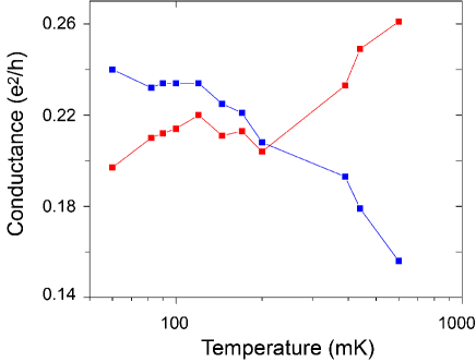
The temperature dependences of the zero-bias conductance in the centers of the (1,1) and (2,1) charge regions are shown in Fig. S2. They can readily be explained with reference to Fig. 1(c) of the main text, noting that the dominant effect of increasing temperature is to broaden the low-energy conductance peaks. In the center of the (1,1) region (red points) there is a gradual increase of zero-bias conductance with temperature, corresponding to a filling-in of the conductance dip in the third panel of Fig. 1(c). In the (2,1) region (blue points) by contrast, the broadening of the single conductance peak (2nd panel of Fig. 1(c)) with temperature results in a gradual decrease in the zero-bias conductance. NRG results for similar parameters (not shown) display the same qualitative trends.
III Varying dot-lead and dot-dot coupling strengths
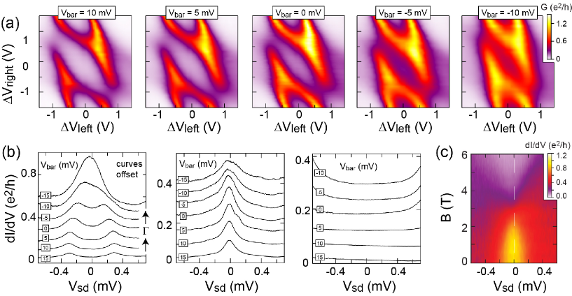
By varying the barrier gate voltage we were able to tune both the interdot coupling and the coupling between the dot and leads. Which of these two effects dominates varies between different electronic states, the microscopic details of which are not presently understood. Nevertheless, the effects are highly reproducible and can be used to investigate the competition between exchange and Kondo correlations on the quantum dots.
Figure S3 shows the stability and differential conductance in the center of the (1,1) charge region as is varied - an extension of Fig. 4 in the main text. In this case, the main effect of varying is an increase in the coupling to the leads. This is deduced from the increase in width (FWHM) of the Coulomb blockade peaks in the stability diagram as well as the increased width of the Kondo resonance observed in the (2,1) charge region, see middle panel of Fig. S3(b). The double peaks in the center of the (1,1) charge region broaden with decreasing to form a single broad peak centered around , interpreted as a crossover to the weakly correlated regime where , see main text.
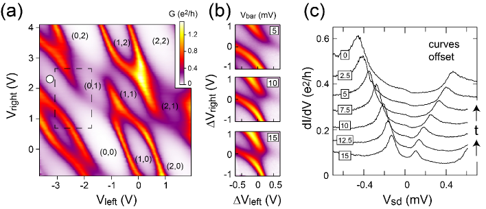
A different dependence on is observed for the neighboring ‘effective’ (1,1) charge region, see Fig. S4. As expected, a double peak structure is observed in the differential conductance. However, in this case, the interdot coupling is changed, resulting in a decrease of the exchange energy with increasing and correspondingly smaller peak splitting, see Fig. S4(c). The change in is also evident in the stability diagram, see Fig. S4(b), where it is observed as a decrease in the separation (and curvature) of the triple points. The smallest peak splitting in the differential conductance was observed for mV, see Fig. S4(c). No further decrease in was observed by increasing beyond this value (not shown).
IV Model Hamiltonian
The canonical model used to describe tunnel-coupled DQDs is the two-impurity Anderson model Salex:64 ; Sgott:64 ; Syama:79 ; Sjaya:82 . We take this as the basic model for our NRG calculations, and supplement it with an interdot Coulomb repulsion/electrostatic coupling term (), which inevitably exists, and which we find necessary to obtain good agreement between theory and the experimental stability diagram shown in Fig. 1(b).
The Hamiltonian, , consists of terms for the isolated leads and dots, and respectively, together with a hybridization term, , describing electron tunneling between dot- () and lead-. The leads, for which
| (1) |
consist of equivalent bands of non-interacting electrons with single-particle energies and spin (where creates a -spin electron in state of lead ). As usual for metallic leads Swils:75 ; Skris:80 ; Skris2:80 ; Sbull:08 , we take the leads to be flat bands with half-bandwidth . For the dots,
| (2) |
where is the number operator for -spin electrons on dot , and . is the single-particle level energy for dot-, the interdot tunnel coupling, the on-dot charging energy/Coulomb repulsion, and the interdot Coulomb interaction. The hybridization term coupling the dots to the leads is given by
| (3) |
with tunnel-coupling to lead-. The strength of hybridization to lead- is embodied in , where is the (uniform) total density of states of the lead, and the number of lead-orbitals ( in the continuum limit). The effect of a magnetic field is readily encompassed by adding , with the total -component of spin on the dots, the magnetic field strength, and the electron -factor. We have taken in comparing to experiment, but note that a slightly smaller value would lead to even better agreement between experiment and theory in Fig. 3 of the paper.
In our calculations we use the parameters and determined experimentally, and a temperature mK. Experimentally, the dot level energies are controlled by two gate voltages, and . One might naively anticipate but, as is physically natural given the experimental set-up (Fig. 1(a)), there is some ‘cross talk’ between the side gate voltages, and to obtain good agreement between experiment and theory it is necessary to include some dependence of on and of on . Specifically, we find
| (4) |
with giving the best agreement.
V NRG calculation of conductance
We use the full density matrix (FDM) formulation Spete:06 ; Sweic:07 of the NRG Swils:75 ; Skris:80 ; Skris2:80 (for a recent review see Ref. Sbull:08, ), keeping around 2000 states per iteration. To reduce discretization error, we average over different lead discretizations and calculate the dot Green functions via the self-energy method Sbull:98 . This enables us to work reliably with a relatively large discretization parameter of .
To calculate the zero-bias () conductance, , of the model at finite temperature, we use an exact Kubo-type current-current correlation function approach, derived via linear-response theory Ssaka:97 ; Ssaka:2000
| (5) |
where (with )
| (6) |
The correlation functions , which can be calculated directly via the FDM-NRG, are given by
| (7) |
where denotes an anticommutator and is the unit step function. The , defined by
| (8) |
are current operators (modulo constants), with the operator for the zero-orbital of the Wilson chain representation of lead Swils:75 ; Skris:80 ; Skris2:80 . At , the zero-bias conductance eqs.5-8 takes the simpler, physically intuitive form Sgeor:99
| (9) |
Here is the off-diagonal (or interdot) retarded Green function, , which may also be calculated via the FDM-NRG; and denotes the zero-bias Fermi level. Results for the conductance obtained this way agree very well (as they should) with those calculated using eqs.5-8 as .
At finite bias nothing exact can be said and, in practice, approximations must inevitably be made. Here we make the common approximation of bias-independent self-energies (which as judged by previous comparison to experiment Sgalp:10 ; Sande:08 ; Sloga:09 appears quite successful), and approximate the finite-bias conductance by
| (10) |
where is the Fermi function for lead , with chemical potentials and . The quantity () is a measure of how the voltage bias is partitioned between the leads; being perfectly symmetric, and or meaning the bias is applied entirely on one lead. We take throughout, this value being found to give the best agreement with the experimental data (in particular for the slopes of the Coulomb blockade peaks, which are known to depend on Slogan:JCP ; Swright:11 ).
References
- (1) S. J. Chorley, M. R. Galpin, F. W. Jayatilaka, C. G. Smith, D. E. Logan and M. R. Buitelaar (unpublished).
- (2) J. Kong, A. Cassell and H. Dai, Chem. Phys. Lett. 292, 567 (1998).
- (3) S. Alexander and P. W. Anderson, Phys. Rev. 133, A1594 (1964).
- (4) P. Gottlieb and H. Suhl, Phys. Rev. 134, A1586 (1964).
- (5) K. Yamada, Prog. Theor. Phys. 62, 901 (1979).
- (6) C. Jayaprakash, H. R. Krishnamurthy, and J. W. Wilkins, J. Appl. Phys. 53, 2142 (1982).
- (7) K. Wilson, Rev. Mod. Phys., 47, 773-840 (1975).
- (8) H. R. Krishnamurthy, J. W. Wilkins and K. G. Wilson, Phys. Rev. B, 21, 1003-1043 (1980).
- (9) H. R. Krishnamurthy, J. W. Wilkins and K. G. Wilson, Phys. Rev. B, 21, 1044-1083 (1980).
- (10) R. Bulla, T. A. Costi and T. Pruschke, Rev. Mod. Phys., 80, 395 (2008).
- (11) R. Peters, T. Pruschke and F. B. Anders, Phys. Rev. B, 74, 245114 (2006).
- (12) A. Weichselbaum and J. von Delft, Phys. Rev. Lett., 99, 076402 (2007).
- (13) R. Bulla, A. C. Hewson and T. Pruschke, J. Phys.: Condens. Matter, 10, 8365-8380 (1998).
- (14) W. Izumida, O. Sakai, and Y. Shimizu, J. Phys. Soc. Jpn. 66, 717 (1997).
- (15) W. Izumida and O. Sakai, Phys. Rev. B, 62, 10260 (2000).
- (16) A. Georges and Y. Meir, Phys. Rev. Lett., 82, 3508-3511 (1999).
- (17) M. R. Galpin, F. W. Jayatilaka, and D. E. Logan, Phys. Rev. B 81, 075437 (2010).
- (18) F. B. Anders, D. E. Logan, M. R. Galpin, and G. Finkelstein, Phys. Rev. Lett. 100 086809 (2008).
- (19) D. E. Logan, C. J. Wright, and M. R. Galpin, Phys. Rev. B 80, 125117 (2009).
- (20) D. E. Logan and M. R. Galpin, J. Chem. Phys. 130, 224503 (2009).
- (21) C. J. Wright, M. R. Galpin and D. E. Logan, Phys. Rev. B 84, 115308 (2011).