symmetric electronics
Abstract
We show both theoretically and experimentally that a pair of inductively coupled active LRC circuits (dimer), one with amplification and another with an equivalent amount of attenuation, display all the features which characterize a wide class of non-Hermitian systems which commute with the joint parity-time operator: typical normal modes, temporal evolution, and scattering processes. Utilizing a Liouvilian formulation, we can define an underlying -symmetric Hamiltonian, which provides important insight for understanding the behavior of the system. When the -dimer is coupled to transmission lines, the resulting scattering signal reveals novel features which reflect the -symmetry of the scattering target. Specifically we show that the device can show two different behaviors simultaneously, an amplifier or an absorber, depending on the direction and phase relation of the interrogating waves. Having an exact theory, and due to its relative experimental simplicity, -symmetric electronics offers new insights into the properties of -symmetric systems which are at the forefront of the research in mathematical physics and related fields.
pacs:
11.30.Er, 05.60.-k, 45.05.+x1 Introduction
Among the many recent developments in systems, the application of pseudo-Hermitian ideas into the realm of electronic circuitry not only promises a new generation of electronic structures and devices, but also provides a platform for detailed scrutiny of many new concepts within a framework of easily accessible experimental configurations. A first example of this was the demonstration in Ref. [1] that a pair of coupled circuits, one with amplification and the other with equivalent amount of attenuation, provided the simplest experimental realization of a symmetric system. With a normal mode structure where all dynamical variables are easily measured in the time domain, extensions of the circuit approach will provide a valuable testing ground for further developments into more sophisticated structures. Moreover, the -circuitry approach suggested also opens new avenues for innovative electronics architectures for signal manipulation from integrated circuits to antenna arrays, and allows for direct contact with cutting edge technological problems appearing in (nano)-antenna theory, split-ring resonator arrays, and meta-materials.
Examples of -symmetric systems range from quantum field theories and mathematical physics [2, 3, 4, 5] to atomic [6, 7], solid state [8, 9, 10] and classical optics [11, 12, 13, 14, 15, 16, 17, 18, 19]. A -symmetric system can be described by a phenomenological ”Hamiltonian” which may have a real energy spectrum, although in general is non-Hermitian. Furthermore, as some parameter that controls the degree of non-Hermiticity of changes, a spontaneous symmetry breaking occurs. At this point, , the eigenfunctions of cease to be eigenfunctions of the -operator, despite the fact that and the -operator commute [2]. This happens because the -operator is anti-linear, and thus the eigenstates of may or may not be eigenstates of . As a consequence, in the broken -symmetric phase the spectrum becomes partially or completely complex. The other limiting case where both and share the same set of eigenvectors corresponds to the so-called exact -symmetric phase in which the spectrum is real. This result led Bender and colleagues to propose an extension of quantum mechanics based on non- Hermitian but -symmetric operators [2, 3]. The class of non-Hermitian systems with real spectrum has been extended by other researchers in order to include Hamiltonians with generalized (antilinear) symmetries [20].
While the applicability of these ideas in the quantum framework is still being debated, optical systems provide a particularly fertile ground where -related concepts can be realized [11] and experimentally investigated [13, 14]. In this framework, symmetry demands that the complex refractive index obeys the condition . -synthetic materials can exhibit several intriguing features. These include among others, power oscillations and non-reciprocity of light propagation [11, 14, 16], absorption enhanced transmission [13], and unidirectional invisibility [18]. Despite these efforts and the consequent wealth of theoretical results associated with -structures, until very recently only one experimental realization of a system with balanced gain and loss has been reported [14]. These authors studied the light propagation in two coupled symmetric waveguides where the spontaneous -symmetry breaking “phase transition” [21] was indirectly confirmed. The analysis relied on the paraxial approximation which under appropriate conditions maps the scalar wave equation to the Schrödinger equation, with the axial wavevector playing the role of energy and with a fictitious time related to the propagation distance along the waveguide axis.
This observation led us recently to propose a new set-up based on active LRC circuits where the novel features of - symmetric structures can reveal themselves and can be studied both theoretically and experimentally in great detail. The system consists of a pair of coupled electronic oscillators, one with gain and the other with loss. This ”active” dimer, is implemented with simple electronics, and allow not only for a direct observation of a spontaneous -symmetric “phase transition” from a real to a complex eigenfrequency spectrum but also for its consequences in the spatio-temporal domain. At the same time the equivalent scattering system, where a localized symmetric structure is connected to one or two transmission line (TL) leads allow us to access the validity of recent theoretical predictions [17, 22, 23, 24, 25, 26, 27, 28].
This paper presents our recent results pertaining to the electronics. We begin with a general discussion of electronics in the context of symmetric systems in section 2. Then in section 3 we examine the normal mode structure of the simplest such circuit, the dimer. We experimentally demonstrate how it displays all the novel phenomena encountered in systems with generalized -symmetries. Section 4 discusses the unique aspects of dynamics exhibited by the dimer, particularly upon passage from the exact to broken phase. In section 5 we investigate the simplest possible scattering situation where the dimer is coupled to a single TL, and derive a non-unimodular conservation relation connecting the left and right reflectances. A direct consequence of this relation is the existence of specific frequencies for which the system behaves either as a perfect absorber or as an amplifier, depending on the side (gain or loss) to which the TL is coupled. In section 6 we demonstrate theoretically and experimentally that a two-port -symmetric electronic cavity can act as a simultaneous coherent perfect absorber (CPA)-amplifier. Our circuit is the electronic equivalent of a CPA-Laser device which was recently proposed in the optics framework, and constitutes the first experimental realization of such devices. Finally, section 7 presents several issues involving practical implementation of circuits, along with some related experimental details. Our conclusions are given in section 8.
2 electronics
One of the most convenient advantages of an electronic approach is that, at least in the low frequency domain, where the wavelength is significantly greater than the dimensions of the circuit, all spatial symmetry considerations can be reduced to a matter of network topology defined through the application of Kirchoff’s laws. Physical symmetry is irrelevant as long as the network has the desired node topology and the connecting elements are appropriately valued. Analogous to the familiar case of a -symmetric potential, the parity operation is equivalent to the interchange of labels corresponding to pairs of associated circuit components.
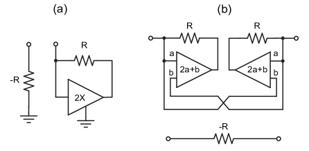
For simplicity, we will restrict our discussion to the usual fundamental physical devices: resistors, capacitors and inductors. Only the resistor, due to it’s dissipative nature, requires modification upon time-reversal where we include generic Ohmic elements with either positive or negative resistance. Negative resistance represents the simplest conceptual inclusion of amplification into electronics since Kirchoff’s laws can be used without modification. Fig. 1 illustrates how simple linear amplifiers can be configured to achieve negative resistance. The schematic implementation in (a) results in a single, ground-referenced node, while that in (b) shows a true two-terminal configuration. The former is of greatest utility due to it’s simplicity and the pervasiveness of ground nodes (defining a common zero potential) in typical circuits. Section 7 discusses further details of the experimental negative resistance converters.
Theoretical analysis of circuits including negative resistance elements, however, requires respecting a subtle condition: any two terminal circuit structure reducing to a pure negative resistance will be undefined unless the structure is placed in parallel with a capacitance. This conclusion results from the divergence of the pole associated with parallel combinations (with negative ) in the limit of . This pole only arises if parallel capacitance is initially considered, so is hidden, and often overlooked in the consideration of negative resistance circuits. It is inconsequential with normal, positive resistance, where it’s sign corresponds to exponential decay. For example, the standard series circuit, though it appears to have a mathematically well behaved solution for negative , is invalid in that realm due to the hidden pole. Our choice of the parallel configurations was dictated by this consideration.
Thus, for a -symmetric circuit incorporating these basic elements, it is necessary that (1) all reactive elements either have representation in parity-associated network pairs, or connect parity inverted network nodes, (2) all Ohmic elements are paired with opposite sign, and (3) each negative Ohmic element has an associated parallel capacitance, or AC equivalent, as part of the circuit. Valid -circuits of arbitrary complexity can be built up using these simple rules, though their stability needs to be independently determined. In principle, the long-wave approximation could be relaxed with an appropriate inclusion of waveguide connections, however, this would return geometry into the mix of considerations.
3 dimer modes
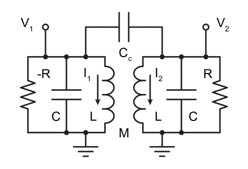
Figure 2 shows the -symmetric dimer, the simplest configuration with a non trivial (more than one mode) pseudo-Hermitian spectrum. Both capacitive and mutual inductive coupling are included for generality, although the experimental results presented throughout this work are exclusively one or the other. The gain side on the left of Fig. 2 is indicated by and was implemented using the configuration of Fig. 1(a). The loss on the right is achieved with a conventional resistance of the same value, resulting in the gain/loss parameter for this system. Further details of the experimental circuit are given in section. 7.
Kirchoff’s laws for the dimer with both mutual inductance coupling and capacitive coupling between the oscillators are given for the gain side (Eq. (1)) and loss side (Eq. (2)).
| (1) | |||
| (2) |
Eliminating the currents from the relations, scaling frequency and time by , and taking and gives the matrix equation:
| (3) |
At this point, it is obvious that the system is symmetric: swapping the indices and changing the sign of leaves the equations unchanged. This linear, homogeneous system has four normal mode frequencies, as required to fulfill any arbitrary initial condition for voltage and current, given by
| (4) |
with the symmetry breaking point identified as
| (5) |
and the upper critical point by
| (6) |
Note that the given forms explicitly show all of the relationships among the critical points and the real and imaginary parts of the frequencies. The exact phase, , is characterized by four purely real eigenfrequencies coming in two pairs of positive () and negative () values, while in the broken phase below the upper critical point, the eigenfrequencies are coming in complex conjugate pairs with non-vanishing real parts, and above , as two purely imaginary complex conjugate pairs. The broken phase of the dimer is unstable, in that it is ultimately dominated by an exponentially growing mode.
The normal modes in the exact phase are characterized by equal magnitudes for the voltage oscillations in the gain and loss sides, which in the , real part convention allowed by the real eigenfrequencies, are given by
| (7) |
with a phase of the loss side
| (8) |
As the gain/loss parameter traverses the exact region, , the phase progresses from the in- and out-of-phase configuration of a Hamiltonian coupled oscillator, to a mode coalescence at with with the real frequency
| (9) |
Examination of the inductor currents,
| (10) |
reveal phase shifts, relative to the corresponding voltages, that advance on the gain side and retard on the loss side within either mode. This is as required for the net transfer of electrical energy from the gain side to the loss side as the gain/loss parameter increases. This evolutionary behavior is helpful in understanding the spectral and dynamical behavior of the dimer.
An alternate analysis of the dimer is also accomplished by recasting Kirchoff’s laws, Eqs. (1) and Eq. (2) into a “rate equation” form by making use of a Liouvillian formalism
| (11) |
where , , and with . This formulation opens new exciting directions for applications [29] of generalized -mechanics [20] as it can be interpreted as a Schrödinger equation with non-Hermitian effective Hamiltonian . This Hamiltonian is symmetric with respect to generalized transformations [29], i.e. , where
| (12) |
and is the Pauli matrix, is the identity matrix, and denotes the operation of complex conjugation. By a similarity transformation [29],
| (13) |
can be related to a transposition symmetric, symmetric Hamiltonian , where . The matrix is then
| (14) |
where , and . The frequencies and normal modes within this framework are identical to Eqs. (4,10).
These normal mode properties can be measured in our electronic dimer by simultaneous observation of the node voltages and of Fig. 2. Our set-up allows detailed analysis for gain/loss parameters on either side of the -phase transition point. In the exact phase, time series samples are captured with the dimer slightly unbalanced to marginally oscillate the mode of interest. Beyond the critical point, a transient sample is obtained dominated by the exponentially growing mode. Details are given in section 7.
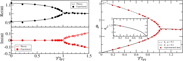
In Fig. 3 we report measurements for the dimer frequencies (left) and inter-component phases (right) compared with the theoretical expressions, Eq. (4) and Eq. (8) respectively, for the values and . The symmetry imposes the condition that the magnitude of the two voltage components are equal to one-another in the exact phase. This property is also experimentally observed. For , the phases corresponding to the symmetric and antisymmetric combination are and , respectively. When is subsequently increased and the system is below the threshold, the eigenstates are not orthogonal and their phases can be anywhere (depending on ) in the interval .
The value of phase difference at the spontaneous -symmetric breaking point can be calculated analytically and it is given by the expression:
| (15) |
We note that in the limit of we get , corresponding to a ”circular” polarization of the eigenmode. The opposite limit of results to corresponding to ”linear” polarization.
4 dimer dynamics
The signatures of -symmetry and the transition from the exact phase to the broken phase are similarly reflected in the temporal behavior of our system. Eq. (11) can be solved either analytically or via direct numerical integration in order to obtain the temporal behavior of the capacitor charge and the displacement current in each of the two circuits of the -symmetric dimer. As an example of the dimer state evolution, we consider an initial displacement current in one of the circuits with all other dynamical variables zero.
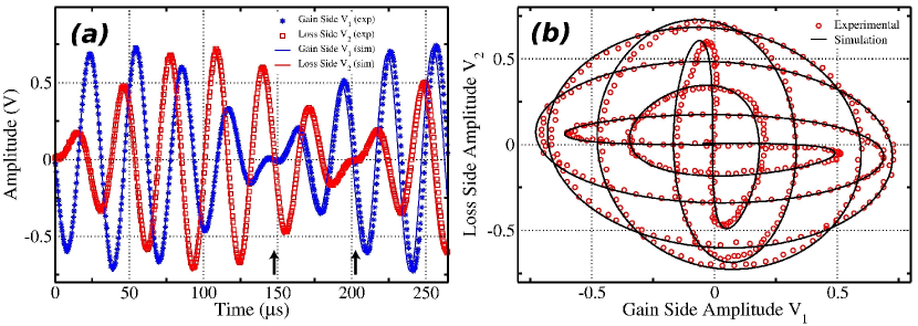
In Fig. 4 we present some typical measurements for the temporal behavior of circuit voltages along with the corresponding numerical result. We consider a dimer configuration with and (i.e. inductive coupling only). In the left panel of Fig. 4a, we show and for an initial condition having with all other dynamical variables zero. The right panel shows the same data as a Lissajiou plot, with the initial condition trajectory leaving the origin with decreasing, and stationary. Agreement between the experiment (circles) and the simulations (lines) is observed, illustrating that, in spite of the presence of dissipative elements and non-orthogonal states, the beat superposition associated with real frequencies occurs. There is, however, a subtle distinction: Since energy is not conserved, the beat is asymmetric between the gain side and the loss side nodal times, with oscillatory activity spending more time between gain side nodal points as energy grows to a significantly larger size before decaying and growing between the loss side nodal points. However, unlike traditional coupled-oscillator beats, instead of “slashing” between both sides during the course of the beats, a growth and decay energy dance occurs with both sides more or less equally represented except in the vicinity of the nodal points. This behavior is a direct result of the non-orthogonal phase relationships that become more pronounced as . A Hamiltonian dimer would exhibit a perfect half-beat offset between the left and right voltage beat envelopes.
We have also traced these energy dance features by studying the time-dependence of the total capacitance energy:
| (16) |
With the initial condition used in the experiment, we expect power oscillations which are due to the unfolding of the non-orthogonal eigenmodes [2, 11, 16, 14]. This universal feature is evident in the temporal behavior of as can be seen in Fig. 5. On the other hand, for the dynamics is unstable and grows exponentially with a rate given by the maximum imaginary eigenvalue (see Fig. 5).
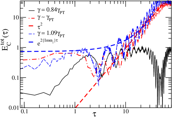
The most interesting behavior appears at the spontaneous -symmetry breaking point . At this point the matrix has a defective eigenvalue. In this case, the evolution can be calculated from the Jordan decomposition of as . Having in mind the form of the exponential of a Jordan matrix, it follows immediately that linear growing terms appear in the evolution of the charge vector [30]. This results in a quadratic increase of the capacitance energy i.e. . Although all systems typically becomes very sensitive to parameters near a critical point, we are able to control the circuit elements sufficiently well to observe the approach to the predicted behavior of the energy. This time range is limited by the dynamic range of our circuit linearity, as discussed in section 7
5 The Janus faces of -symmetric scattering
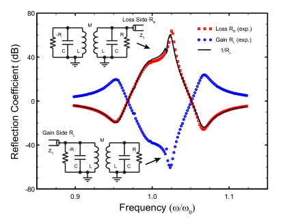
We report our initial scattering studies with the following two reciprocal geometries: In the first case, a transmission line (TL) is attached to the left (amplified) circuit of the dimer load while in the second case, the TL is connected to the right (lossy) circuit of the load (see lower and upper insets of Fig. 6 respectively). Experimentally, the equivalent of a TL with characteristic impedance could be attached to either side of the dimer at the circuit voltage node in the form of a resistance in series with a variable frequency voltage source. The right and left traveling wave components associated with the TL would be deduced from the complex voltages on both sides of . With the voltage on the circuit, and the voltage on the synthesizer side of the coupling resistor , the right (incoming) wave has a voltage amplitude and the left (reflected) wave has a voltage amplitude . The voltage source defines the phase of the incoming wave.
At any point along a TL, the current and voltage determine the amplitudes of the right and left traveling wave components [31]. The forward and backward wave amplitudes, and and the voltage and current at the left or right TL-dimer contacts satisfy the continuity relation
| (17) |
which connect the wave components to the currents and voltages at the TL-dimer contact points. Note that with this convention, a positive lead current flows into the left circuit, but out of the right circuit, and that the reflection amplitudes for left or right incident waves are defined as and respectively.
Application of Kirchoff’s laws at the TL leads allow us to find the corresponding wave amplitudes and reflection. For this analysis, we assume the wave convention. For example, the case of the left-attached lead in the lower inset of Fig. 6 gives
| (18) | |||
where is the dimensionless TL impedance, and are the current amplitudes in the left or right inductors. These are equivalent to the simple dimer form Eq. (1) and Eq. (2) with the addition of the contact current and the opposite sign convention for more appropriate for the traveling wave analysis. Similar equations apply for the right-attached case shown in the upper inset of Fig. 6. We are interested in the behavior of the reflectance , as the gain/loss parameter , and the frequency changes.
For -symmetric structures, the corresponding scattering signals satisfy generalized unitarity relations which reveal the symmetries of the scattering target. Specifically, in the single-port set up this information is encoded solely in the reflection. To unveil it, we observe that the lower set-up of Fig. 6 is the -symmetric replica of the upper one. Assuming therefore that a potential wave at the left lead (lower inset) has the form (we assume and in Eq. (17)), we conclude that the form of the wave at the right lead associated with the upper circuit of Fig. 6 is . Direct comparison leads to the relation
| (19) |
where are the left/right reflection phases. Note that Eq. (19) differs from the more familiar conservation relation , which applies to unitary scattering processes as a result of flux conservation. In the latter case left and right reflectances are equal. Instead in the -symmetric case we have in general that [32].
For the specific case of the -symmetric dimer, we can further analytically calculate the exact expression for the reflection coefficients. From Eqs. (5) we have
| (20) | |||
In the limiting cases of the reflection amplitude becomes and thus unitarity is restored.
In the main panel of Fig. 6 we plot the reflection coefficients of Eq. (5) for the two scattering configurations shown in the sub-panels. The measured reflectances , and satisfy the generalized conservation relation as expected from Eq. (19). The slight deviation from reciprocity in the vicinity of large reflectances can be attributed to nonlinear effects.
A peculiarity of our results is the appearance of a singularity frequency point for which , while a reciprocal point for which is also evident. The corresponding are found from Eq. (5) to be
| (21) |
Therefore, our experiment demonstrates that a -symmetric load is a simple electronic Janus device that for the same values of the parameters acts as a perfect signal absorber as well as a signal amplifier, depending on the side (gain or loss) that the TL is coupled to the dimer.
6 Two-port coherent perfect absorber-amplifier
Recent theoretical studies in the optics framework [17] have suggested that a two-port -symmetric cavity can act as a simultaneous coherent perfect absorber (CPA)-laser. In this section we provide the first experimental realization of this proposal using a two-port configuration of our -symmetric electronic dimer, and demonstrate it’s action as simultaneous CPA-amplifier. We consider the capacitively coupled case, with as previously defined, to demonstrate the independence of the generic behavior from the coupling mechanism. Following steps similar to the single-port case, Kirchoff’s laws lead to the following set of equations:
| (23) | |||
| (24) |
The above equations can be written in a more elegant form by making use of the transfer matrix formulation:
| (31) |
where the transfer matrix elements are , , , and , with . One can further express the spectral transmission and reflection coefficients for left (L) and right (R) incidence in terms of the transfer matrix elements as [26, 27]
| (32) |
where we have used the identity that .
An alternative formulation of the transport problem utilizes the so-called scattering matrix which connects incoming to outgoing waves and its elements can be written in terms of the transmission/reflection coefficients. Specifically
| (39) |
Using the scattering matrix language one can derive conditions in order our -symmetric structure to act either as an amplifier or as a perfect absorber. For a laser oscillator without an injected signal, the boundary conditions apply, which imply from Eq. (39) the condition [27]. In contrast, for a perfect absorber the boundary conditions, , corresponding to zero reflected waves, hold. From Eq. (39) this implies , while the amplitudes of the incident waves must satisfy the condition . In general, the condition for an amplifier/laser system, is not satisfied simultaneously with the condition for a perfect absorber. However for any -symmetric structure, one can show from Eq. (31) that the matrix elements of satisfy the relation [17]. As a result, a real exists, that satisfies the amplifier/laser condition simultaneously with the absorber condition (). Hence the two-port -symmetric dimer can behave simultaneously as a perfect absorber and as an amplifier. This property can be explored using an overall output coefficient defined as [17]
| (40) |
Note that in the case of a single-port scattering set-up discussed earlier in this section, the -function collapses to the left/right reflectances. We can further simplify the above expression using Eq. (31), together with the property . We get
| (41) |
At the singularity frequency point and for a generic ratio , the -function diverges as and the circuit acts as an amplifier/laser. If on the other hand, we assume that (perfect adsorbtion condition), we get
| (42) | |||||
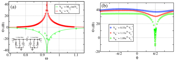
In the context of electronics, the two port simultaneous laser/absorber properties are manifest as a delicate balance of the driven, marginally stable circuit. The singular behavior of the theoretical in Fig. 7(a), solid curves, illustrate that at the Janus frequency the injected signals can result in either amplification or complete attenuation, depending on the relative amplitude and phase of the injected signals. The perfect absorption condition is particularly sensitive to the injection parameters: the deviation of the experimental data, Fig. 7(a) dots, is characteristic of component imbalance of less than . In fact, the minimally absorbing experimental points near the dip in the attenuation curve of Fig. 7(a) can only be obtained by an independent determination of the minimal reflectance condition at each frequency. Fig. 7(b) shows this extreme sensitivity to the phase of the right input signal near and illustrates our current experimental limits to the observation of the Janus condition.
7 Practical considerations
Although the fundamental theoretical aspects of electronic circuits is straightforward, it is important to realize that all physical electronic elements deviate from their ideal intended function in two distinctly different ways. First, all have unintentional or stray impedances – resistive and reactive components – that can become significant as frequency changes. Second, all components, particularly amplifiers, are subject to linearity limits.
The experimental dimer, equivalent to that shown in Fig. 2 with either the inductive or capacitive coupling, consists of a pair of coupled circuits, one with amplification in the form of the negative resistance, and the other with equivalent attenuation. The circuit was shown in Ref. [1] to be a simple realization of the -symmetric dimer. Each inductor is wound with turns of #28 copper wire on diameter PVC forms in a loose bundle for an inductance of . The coils are mounted coaxially with a bundle separation adjusted for the desired mutual inductance . The isolated natural frequency of each coil is .
The actual experimental circuit includes several additions to that of Fig. 2 acknowledging the physical realities mentioned above. First, a resistive component associated with coil wire dissipation is nulled by an equivalent Ohmic gain component applied in parallel to each coil. A discussed in section 2, it is not possible to directly apply a series Ohmic gain for this compensation. This is our dominant deviation from ideal behavior, however, we have determined from simulation that compensating for this series loss by a parallel gain has negligible impact on the ideal behavior.
Second, additional LF356 op-amps, also used for the negative resistance converter of Fig. 1(a), are used for voltage followers to buffer the voltages and of Fig. 2, allowing for a less intrusive capture with the Tektronix DPO2014 oscilloscope used for signal acquisition.
Finally, small capacitance and gain trims are included to aid in circuit balancing.
Our linearity is constrained by the LF356 op-amps in the negative impedance converters of Fig. 1a. At the operating frequency, the limits were consistent with the supply voltage used for the circuit. In fact, the op-amp linearity limited the overall operation frequency of the dimer: higher frequency op-amps are available, but their linearity and input impedance suffer.
The linear nature of our system allows an exact balance of the symmetry only to the extent that component drift over a time scale necessary to perform a measurement is negligible. In the exact phase, real system modes are not perfectly achievable: in time, any physical linear system ultimately either shrinks to zero or exponentially grows to the physical linearity limit. In the case of our dimer, component precision and drift dictate the accuracy of the balance to approximately , and all data was obtained respecting the linearity limits and associated transient time scales.
Experimental practice allows for only a marginal determination gain/loss balance. The chosen gain/loss parameter is set by the loss-side resistance of Fig. 2, typically in the range for this work. The gain-side and capacitance balance are set with the help of the gain and capacitance trims. In the exact phase, not too close to , the system is trimmed for simultaneous marginal oscillation of both modes with growth or decay times greater than , where data is then obtained. The imaginary frequency component is then zero to within .
Very close to the critical point, attempts to trim the dimer to the marginal configuration result in either (the gain too small), or a chaotic interplay of the two modes with the op-amp nonlinearity if the gain is larger. This behavior serves as one indication that the critical point has been exceeded. In the vicinity of and beyond, the capacitance trim is kept fixed at its asymptotic value, and the gain trim is numerically set to compensate for any measured deviation of the gain side chosen from the desired value. The exponential growth or decay rate of transient data obtained then directly gives us the imaginary component. Beyond the point, the exponentially growing mode always dominates.
At this point, these experimental techniques ultimately impact the limits to which the theory is applicable, particularly in the vicinity of the symmetry breaking point where small imbalances can drastically impact the dynamics. We anticipate that, due to the stabilizing nature of resistive loads in the form of transmission lines, the dimer will provide many opportunities for incorporation into scattering configurations.
8 Conclusions
The -symmetric dimer opens a new direction towards investigating novel phenomena and functionalities of -symmetric systems in the spatio-temporal domain via electronic circuits. This minimal example, which is experimentally simple and mathematically transparent, displays all the universal phenomena encountered in systems with generalized -symmetries. The direct accessibility to all the dynamical variables of the system enables insight and a more thorough understanding of generic -symmetric behavior. In addition, we envision new opportunities for inclusion of electronics into structures including (nano)-antenna configurations, metamaterials, or microresonator arrays with electronic control over directional signal transmission capabilities and real-time manipulation in the spatio-temporal domain.
Acknowledgments– We acknowledge support by an AFOSR No. FA 9550-10-1-0433 grant, by an NSF ECCS-1128571 grant, and by an Wesleyan Project grant.
References
References
- [1] J. Schindler, Ang Li, Mei C. Zheng, F. M. Ellis, T. Kottos, Phys. Rev. A 84, 040101(R) (2011).
- [2] C. M. Bender and S. Boettcher, Phys. Rev. Lett. 80, 5243 (1998); C. M. Bender, Rep. Prog. Phys. 70, 947 (2007).
- [3] C. M. Bender, S. Boettcher, P. N. Meisinger, J. Math. Phys. 40, 2201 (1999).
- [4] C. M. Bender, D. C. Brody, and H. F. Jones, Phys. Rev. Lett. 89 270401 (2002).
- [5] C. M. Bender, D. C. Brody, H. F. Jones, and B. K. Meister, Phys. Rev. Lett. 98, 040403 (2007).
- [6] M. Hiller, T. Kottos, A. Ossipov, Phys. Rev. A 73, 063625 (2006).
- [7] E. M. Graefe, H. J. Korsch, A. E. Niederle, Phys. Rev. Lett. 101, 150408 (2008); M. K. Oberthaler et. al, Phys. Rev. Lett. 77, 4980 (1996).
- [8] O. Bendix, et. al, Phys. Rev. Lett. 103, 030402 (2009); C. T. West, T. Kottos, T. Prosen, ibid. 104, 054102 (2010).
- [9] O. Bendix et al., J. Phys. A: Math. Theor. 43, 265305 (2010)
- [10] Y. N. Joglekar et. al, Phys. Rev. A 82, 030103(R) (2010).
- [11] K. G. Makris et. al, Phys. Rev. Lett. 100, 103904 (2008); Z. H. Musslimani et. al, ibid. 100, 030402 (2008).
- [12] S. Longhi, Phys. Rev. Lett. 103, 123601 (2009).
- [13] A. Guo, et al., Phys. Rev. Lett. 103, 093902 (2009).
- [14] C. E. Ruter et. al, Nat. Phys. 6, 192 (2010).
- [15] H. Ramezani et. al, Phys. Rev. A 82, 043803 (2010).
- [16] M. C. Zheng et. al, Phys. Rev. A 82, 010103 (2010).
- [17] S. Longhi, Phys. Rev. A 82, 031801(R) (2010); Y. D. Chong, L. Ge, A. D. Stone, Phys. Rev. Lett. 106, 093902 (2011).
- [18] Z. Lin, et. al, Phys. Rev. Lett 106, 213901 (2011).
- [19] A. A. Sukhorukov, Z. Xu, Y. S. Kivshar, Phys. Rev. A 82, 043818 (2010).
- [20] A. Mostafazadeh, J. Math. Phys. 44, 974 (2003).
- [21] We use the term “phase transition” not in the standard thermodynamic sense but rather in the frame of -literature (see for example [2]).
- [22] S. Longhi, Phys. Rev. Lett. 105, 013903 (2010).
- [23] Y. D. Chong, L. Ge, A. D. Stone, Phys. Rev. Lett. 106, 093902 (2011); L. Ge, Y. D. Chong, A. D. Stone, arXiv: 1112.5167 (2011).
- [24] Z. Lin, et. al, Phys. Rev. Lett 106, 213901 (2011)
- [25] H. Schomerus, Phys. Rev. Lett. 104, 233601 (2010).
- [26] F. Cannata, J.-P. Dedonder and A. Ventura, Ann. of Phys. 322, 397 (2007).
- [27] A. Mostafazadeh, Phys. Rev. Lett. 102, 220402 (2009); Phys. Rev. A 80, 032711 (2009); J. Phys. A 42, 125303 (2009).
- [28] Y. D. Chong et. al, Phys. Rev. Lett. 105, 053901 (2010).
- [29] H. Ramezani, J. Schindler, F. M. Ellis, U. Günther, Tsampikos Kottos, Bypassing the bandwidth theorem with symmetry, submitted (2012).
- [30] S. K. Godunov, Ordinary Differential Equations with Constant Coefficients (Am. Math. Society, 1997).
- [31] Z. Lin, J. Schindler, F. M. Ellis, Tsampikos Kottos, Experimental Observation of the Janus faces of -symmetric scattering, Phys. Rev. A 85, 050101(R) (2012)
- [32] Z. Ahmed, Schrödinger transmission through one-dimensional complex potentials, Phys. Rev. A 64, 042716 (2001).