Proximity-effect-induced superconductivity in topological insulator-related material Bi2Se3
Abstract
We have studied the electron transport properties of topological insulator-related material Bi2Se3 near the superconducting Pb-Bi2Se3 interface, and found that a superconducting state is induced over an extended volume in Bi2Se3. This state can carry a Josephson supercurrent, and demonstrates a gap-like structure in the conductance spectra as probed by a normal-metal electrode. The establishment of the gap is not by confining the electrons into a narrow space close to the superconductor-normal metal interface, as previously observed in other systems, but presumably via electron-electron attractive interaction in Bi2Se3.
pacs:
74.45.+c, 73.40.-c, 74.50.+r, 85.25.CpThrough proximity effect (PE) between a superconductor and a normal metal PE_review , pairing correlation between electrons is delivered from the superconducting side to the normal-metal side. PE has been intensely studied over several decades. It is believed that a PE-affected normal metal would remain resistive unless an energy gap is established to prevent the electrons from scattering non-superconducting01 ; non-superconducting02 . According to McMillan McMillan , this energy gap could be established either through electron-electron (e-e) attractive interaction, or by confining the electrons into a narrow space close to the S-N interface (i.e., in a confined S-N structure), where S and N denote superconductor and normal metal, respectively. From the experimental side, the existence of a PE-induced gap PE_gap01 ; PE_gap02 ; PE_gap03 ; PE_gap04 ; JiaJinFeng and the ability of carrying a supercurrent PE_gap04 have long been verified in confined S-N structures. However, in open S-N structures where the electrons in the normal metal are not necessarily confined near the interface, neither the existence of a PE-induced supercurrent-carrying state nor the existence of an energy gap has been verified experimentally by using independent probes/contacts, only a gap-like structure (i.e., not a true superconducting gap) was observed via a tunneling measurement PE_gap05 .
Recently, particular attention has been paid to the proximity effect between an -wave superconductor and a topological insulator (TI) TI1 ; TI2 ; TI3 . An unconventional superconducting state resembling a spinless superconductor is expected to occur at the S-TI interface. And the vortex cores of that state are believed to host Majorana fermions based on which topological quantum computation can be realized MF1 ; MF2 ; MF3 . To explore these novel phenomena experimentally, one would first need to identify the existence of a PE-induced superconducting state at the S-TI interface. So far, a supercurrent has been observed in S-TI-S type of devices such as Al-Bi2Se3-Al Al-Bi2Se3 , W-Bi2Se3-W W-Bi2Se3 , Pb-Bi2Te3-Pb Pb-Bi2Te3 , and Nb-Bi2Te3 Nb-Bi2Te3 . However, since a supercurrent in S-N-S devices can be carried not only by a PE-induced superconducting state, but also by phase-dependent Andreev bound states PE_review ; SNS01 ; SNS02 , with these results we cannot identify the existence of an independent superconducting state in the PE-affected region. Recently, a superconducting energy gap was observed in ultra-thin Bi2Se3 films grown on a superconducting NbSe2 substrate JiaJinFeng . It proves that a PE-induced superconducting state can be formed in Bi2Se3 films when the electrons there are confined to be close to the S-TI interface, similar to those reported in the early literature PE_gap01 ; PE_gap02 ; PE_gap03 ; PE_gap04 . But it would still be interesting to investigate whether a superconducting state can be established in the TI side without the structural confinement to the electrons. And if yes, how far this state could survive away from the S-TI interface.
Here, we report the observation of a PE-induced zero-resistance state in Bi2Se3 over an extended distance of m away from the Pb-Bi2Se3 interface. The critical supercurrent of the zero-resistance state exhibits a Fraunhofer diffraction pattern against magnetic field. Moreover, a gap-like structure has also been observed in the PE-affected region. The results suggest that the PE-affected region can be regarded as a weak and independent superconductor.
Bi2Se3 flakes were exfoliated onto SiO2-Si substrates from a high-quality single crystal. Those with thickness of 100 nm were selected out and further fabricated into devices using a standard e-beam lithography technique. All of the metal films were deposited via magnetron sputtering. The Pb film were deposited lastly, to avoid otherwise being baked at 180∘C during the fabrication of other electrodes, a process which might alloy the Pb-Bi2Se3 interface Pb-Bi2Te3 .
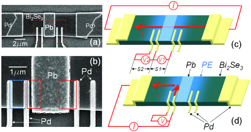
Figure 1 (a) and (b) show the scanning electron microscope (SEM) images of a typical device used in this experiments. A superconducting Pb film was deposited at the center of the Bi2Se3 flake, and two large Pd electrodes were deposited at each end of the flake. Between the Pb film and each of the large Pd electrodes, two small Pd electrodes were deposited, one located close to the Pb film (100 nm away) and the other about 1 m away. These Pd electrodes allow us to perform four-terminal resistance measurement in the PE-affected area on the Bi2Se3 flake, and also to probe the local electronic density of states (DOS) there. We have investigated two devices of this type and obtained very similar results. Investigations on three more devices with a slightly different alignment of Pd electrodes also gave a consistent conclusion. In the following we present the data taken from the device shown in Fig. 1 (a).


Two different measurement configurations were employed, as respectively illustrated in Figs. 1(c) and (d). In order to measure the four-terminal resistance of the PE-affected region, we pass a current through Bi2Se3 crystal from the large Pd electrodes at the two ends. Then the resistance of sections S1 and S2 was measured via corresponding Pd electrodes. While probing the electronic DOS of the PE-affected region, the contact resistance of a small Pd electrode near the Pb film was measured by using a three-terminal configuration. All measurements were carried out in a top-loading dilution refrigerator with a base temperature of 15 mK. Lock-in amplifiers were used, with an ac excitation current of 50 nA and at 30.9 Hz. A Keithley 2400 source-meter was used to drive the superconducting magnet, to guarantee a precise control of magnetic field at milli-Gauss level.
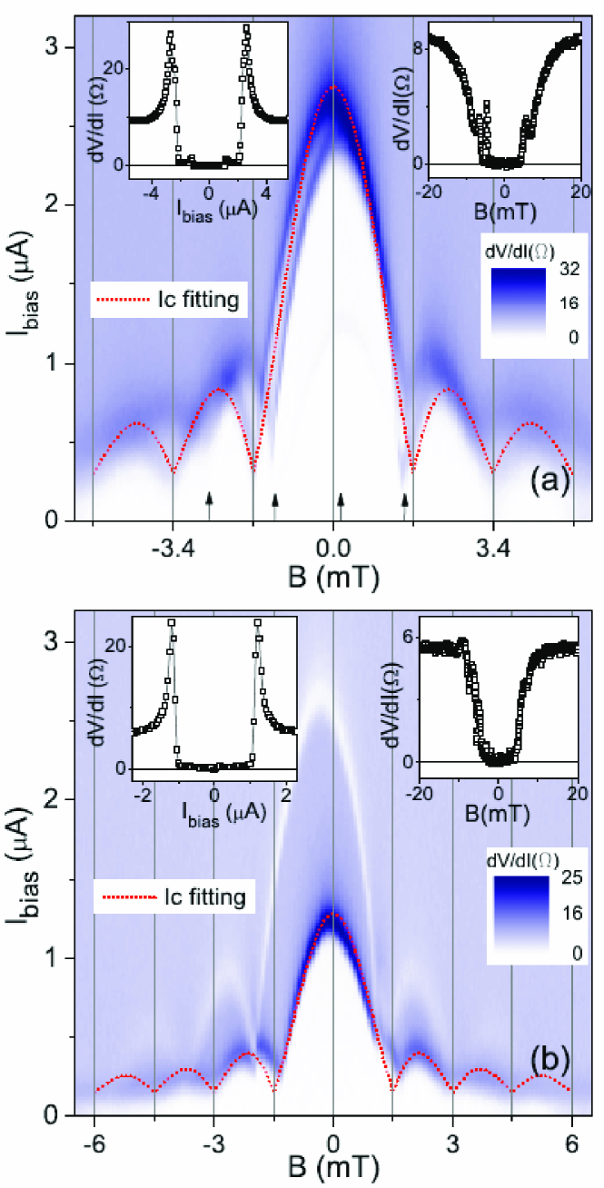
In Figs. 2 (a) and (b) we show the 2D mappings of data as a function of both magnetic field and dc bias current for sections S1 and S2, respectively. The zero magnetic field is determined according to the symmetry of the main structure of the data, which is slightly shifted for different sections, presumably due to local flux pining in the Pb film. A zero-resistance superconducting state was found at low temperatures, represented by the white areas. This state can be destructed by increasing bias current and/or magnetic field, as shown in the insets of Figs. 2(a) and (b). The critical supercurrents vary with applied magnetic field, following a Fraunhofer diffraction pattern. In Fig. 2(a), we can see two sets of Fraunhofer patterns superimposed onto each other, with slightly different periods, as evident in the positions of the pattern minima indicated by the grid lines and the arrows, respectively. We would tentatively ascribe these two sets of patterns to the two S1 sections with different areas at the two sides of the Pb film.
The Fraunhofer pattern shown in Fig. 2(b) was measured across S2. In this region, the induced superconducting state is not as strong as in S1 because of its farther distance from the Pb-Bi2Se3 interface. Therefore, its critical supercurrent is smaller. Because the whole device is at a mesocopic scale, a strong echo from the superconducting transition of S1 can be seen as a thin-white curve in the 2D plot for S2. Similarly, a faint echo from the transition of S2 can also be recognized in Fig 2(a), and is best seen in the left inset of Fig. 2(a) where the conductance undergoes small but sudden increases at A, as marked by the down arrows.
The data can be phenomenologically fitted to a Fraunhofer-like diffraction pattern:
where is the magnetic flux through some effective area, is the flux quanta, and represents the contribution from a part of PE-induced superconducting area which is not included in the effective area causing the oscillation, but is shunted to it. The non-uniform distribution of the PE-induced superconductivity Pb-Bi2Te3 , hence the supercurrent density, might also play a role. The fitting curves are shown in Figs. 2(a) and (b) as red dotted lines. We have =2.45 A and =0.3 A for the fitting in Fig. 2(a), and =1.13 A and =0.15 A for the fitting in Fig. 2(b).
From the fittings we can calculate the effective area of the sections: , where is the period of the Fraunhofer-like pattern. For example, the two periods of 1.7 mT and 1.38 mT shown in Fig. 2(a) correspond to effective areas of 1.22 and 1.50 , respectively, as tentatively ascribed to the two red rectangles in Fig. 1(b). These effective areas appear to be larger than the actual openings between the Pb film and Pd electrodes because of flux compressing and penetration at the edge of the superconducting Pb film. The period of 1.5 mT in Fig. 2(b) corresponds to an effective area of 1.38 , as represented by the blue rectangle in Fig. 1(b). Flux compressing is less pronounced for S2 because this section is located farther from the Pb film. There are more evidences (data not shown) demonstrating that there exist multiple sets of Fraunhofer diffraction patterns, whose periods correspond to some characteristic areas defined by different pairs of normal-metal electrodes. The underline mechanism of this phenomenon is, however, not obvious and warrants further investigations.

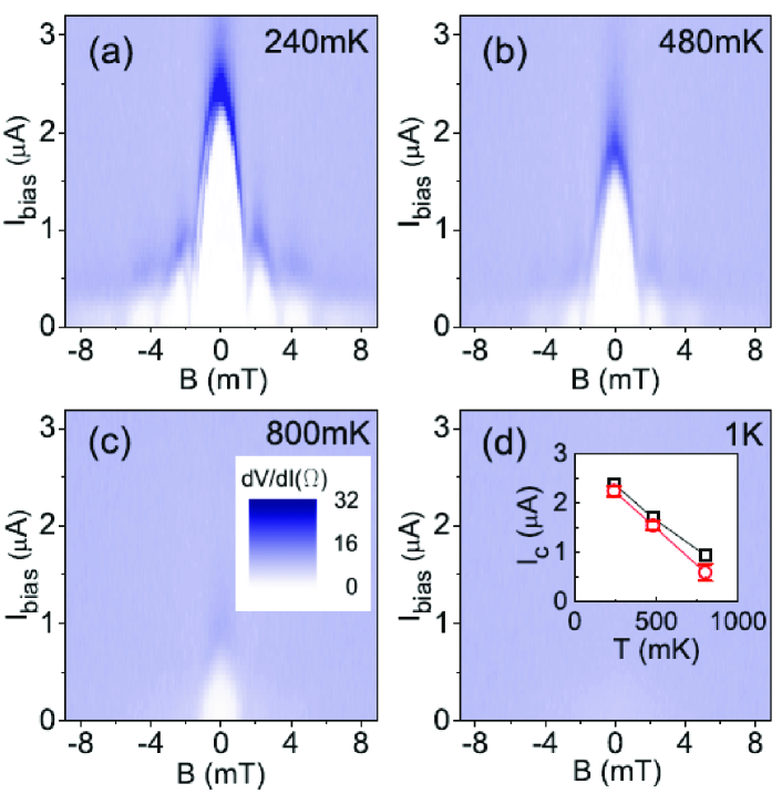
In Fig. 3 we show the 2D plots of the data for S1 measured at different temperatures. The Fraunhofer pattern becomes blurry as temperature increases, and being featureless at =1 K. The zero-field peak height decreases linearly with increasing temperature, as shown in the inset of Fig. 3(d). Similar behavior was also observed on S2 (data not shown), where the data become featureless above =800 mK.

The observed Fraunhofer-like field dependent envelops unambiguously imply that the supercurrents between the Pb and Pd electrodes, and even between two normal-metal Pd electrodes, are all Josephson supercurrents. It also guarantees that the white areas within the envelops represent a superconducting state.
As mentioned in the introduction, in order to sustain a supercurrent in the PE-affected region, there must exist an energy gap; pair correlation alone is not sufficient non-superconducting01 ; non-superconducting02 . According to the theory McMillan , electrons in a PE-affected normal metal must either have an attractive interaction or experience a confinement in order to establish the energy gap. In a recent experimentAu-Al , the synergetic effects of electron confinement and attractive interaction have been revealed by scanning tunneling spectrum studies in Au-Al bi-layer structures. For our device, the Bi2Se3 crystal is long enough (10 m) along the lateral direction from the Pb-Bi2Se3 interface, thus no obvious confinement to the electrons exists. We therefore speculate that the e-e attractive interaction in Bi2Se3 plays a crucial role for the establishment of the gap, and hence the superconducting state, in the PE-affected region.
It has to be noted that, similar to many other experiments on Bi2Se3, the crystal used here is not an intrinsic topological insulator. The Fermi level is shifted into the conduction band due to disorders (mainly Se vacancies) in the sample, so that both the surface states and the bulk states could be involved in/contribute to the proximity effect. Although it is rather unusual that in this experiment the PE-affected region could develop to a distance as far as one micron, which might be attributed to the novelty of the surface states, we are unable to give a definite evidence for this point. On the contrary, our previous work Pb-Bi2Te3 shows that a strong proximity effect develops along the thickness direction of the Bi2Te3 crystal, in addition to along the surface directions of the crystal. Given the fact that Bi2Te3 is very similar to Bi2Se3 in terms of superconducting PE, we conclude that bulk electrons should play an important role in the observed proximity effect, regardless the contribution of the surface electrons.
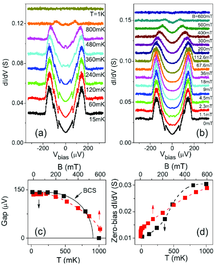
In order to detect the expected superconducting gap in the PE-affected region, we measured the conductance spectra of a small Pd contact 95 nm away from the Pb-Bi2Se3 interface. A three-terminal resistance measurement was performed using the configuration shown in Fig. 1(d). The conductance spectrum, namely the bias voltage dependence of differential conductance, was taken at different temperatures and in different magnetic fields. The results are shown in Figs. 4(a) and (b). The normal-state resistance of the contact is 33.7 . Although it is not in the tunneling limit, according to many experimental studies on S-N junctions S-N-beyond-tunneling , the measured conductance spectrum should partially reflects the DOS of the electrons beneath the contact.
From Fig. 4(a), it is evident that a gap-like structure develops below a critical temperature 1 K, which is much lower than the superconducting transition temperature =7.2 K of Pb. 1 K is also the onset temperature of the Fraunhofer patterns shown in Fig. 3, suggesting a close connection between these two phenomena, behind which is the formation of a PE-induced superconducting phase. Plotted in Fig. 4(c) is the gap value of this phase as a function of temperature. The solid black line is a best fit of the data to the BCS theory. It yields 911 mK.
The gap-like structure disappears in magnetic fields higher than the critical field of the superconducting Pb film, which is about 600 mT for this device [see Fig. 4(b)].
For curves taken in zero magnetic field, there are some jumps inside the gap. While we do not know the origin of these jumps, we speculate that they might arise from some mesoscopic processes with trajectories threaded by magnetic flux, because they are quickly suppressed by raising magnetic field to 1.1 mT. It should be noted that the jumps are not subgap conductance peaks caused by multiple Andreev reflections, which are usually seen in S-N-S junctions.
For the curve taken at 15 mK and in zero field, the peak position of the gap-like structure is 144 V, being only 9.5% of the gap value of Pb. This result confirms our previous result obtained on Sn-Bi2Se3 junctions Sn-Bi2Se3 , where a small gap-like structure occurs at about 1/3 of the gap energy of Sn. It seems to be common that a gap-like structure is induced in the PE-affected regions, with a gap value significantly smaller than that of the maternal superconductor.
Question remains as whether the observed gap-like structure in the conductance spectrum represents a true superconducting gap, since a non-zero subgap conductance (in this experiment, it is about 36% of the normal-state value at 15 mK) could be attributed either to Andreev reflection at the contact BTK , or to a gap-like structure caused by pair correlation in the PE-affected region PE_gap05 ; Usadel01 ; Usadel02 ; Usadel03 . Although the appearance of a supercurrent in our current experiments strongly suggest the existence of a true energy gap, more conclusive data should be obtained via future measurements in the tunneling limit. If a PE-induced gap does exist, Andreev reflection will be greatly suppressed at sufficiently low temperatures in the tunneling limit, resulting in a well-defined gap structure and with a near-zero subgap conductance. Otherwise if the measured gap-like structure is caused by pair correlation, the subgap conductance will remain to be non-zero at low temperatures.
In summary, we have demonstrated that an extended volume in Bi2Se3, up to m away from the Pb-Bi2Se3 interface, can be induced to superconducting through the proximity effect. This superconducting state can carry a Josephson supercurrent, whose critical value oscillates with magnetic field in a Fraunhofer diffraction patten. Since there is no confinement to the electrons in the PE-affected region of Bi2Se3 in our devices, the superconducting gap there, which is needed for stabilizing the induced superconducting state and as has emerged in the measured conductance spectra, is presumably established by e-e attractive interaction in Bi2Se3.
Acknowledgements.
We would like to thank T. Xiang, S. P. Zhao, Z. Fang, X. Dai, C. Ren, L. Shan and X. C. Xie for stimulative discussions. This work was supported by the National Basic Research Program of China from the MOST under the contract No. 2009CB929101 and 2011CB921702, by the NSFC under the contract No. 11174340 and 11174357, and by the Knowledge Innovation Project and the Instrument Developing Project of CAS.References
- (1) B. Pannetier and H. Courtois, J. Low Temp Phys. 118, 599 (2000).
- (2) Yu. V. Nazarov and T. H. Stoof, Phys. Rev. Lett. 76, 823 (1996).
- (3) T. H. Stoof and Yu. V. Nazarov, Phys. Rev. B 53, 14496 (1996).
- (4) W. L. McMillan, Phys. Rev. 175, 537 (1968).
- (5) C. J. Adkins and B. W. Kington, Phys. Rev. 177, 777 (1969).
- (6) S. M. Freaks and C. J. Adkins, Phys. Lett. A 29, 382 (1969).
- (7) J. R. Toplicar and D. K. Finnemore, Phys. Rev. B 16, 2072 (1977).
- (8) A. Kastalsky, L. H. Greene, J. B. Barner and R. Bhat, Phys. Rev. Lett. 64, 958 (1990).
- (9) M.-X. Wang, et al., Science 336, 52 (2012).
- (10) S. Guéron, H. Pothier, N. O. Birge, D. Esteve, and M. H. Devoret, Phys. Rev. Lett. 77, 3025 (1996).
- (11) I. O. Kulik, Sov. Phys. JETP 57, 1745 (1969).
- (12) J. Bardeen and J. L. Johnson, Phys. Rev. B 5, 72 (1972).
- (13) M. Z. Hasan and C. L. Kane, Rev. Mod. Phys. 82, 3045 (2010)
- (14) X.-L. Qi and S.-C. Zhang, Rev. Mod. Phys. 83, 1057 (2011).
- (15) J. E. Moore, Nature 464, 194-198 (2010)
- (16) L. Fu and C. L. Kane, Phys. Rev. Lett. 100, 096407 (2008).
- (17) L. Fu and C. L. Kane, Phys. Rev. B 79, 161408 (2009).
- (18) J. Nilsson, A. R. Akhmerov, and C. W. J. Beenakker, Phys. Rev. Lett. 101, 120403 (2008).
- (19) B. Sacépé, J. B. Oostinga1, J. Li, A. Ubaldini, N. J. G. Couto, E. Giannini and A. F. Morpurgo, Nature Comm. 2, 575 (2011).
- (20) D.-M. Zhang, J. Wang, A. M. DaSilva, J. S. Lee, H. R. Gutierrez, M. H. W. Chan, J. Jain, and N. Samarth, Phys. Rev. B 84, 165120 (2011).
- (21) F.-M. Qu et al., Sci. Rep. 2, 339 (2012).
- (22) M. Veldhorst et al., Nat. Mater. 11, 417 (2012).
- (23) M. Wolz, C. Debuschewitz, W. Belzig, and E. Scheer, Phys. Rev. B 84, 104516 (2011).
- (24) for example, see A. Kastalsky, A. W. Kleinsasser, L. H. Greene, R. Bhat, F. P. Milliken and J. P. Harbison, Phys. Rev. Lett. 67, 3026 (1991).
- (25) F. Yang et al., Phys. Rev. B 85, 104508 (2012).
- (26) G. E. Blonder, M. Tinkham and T. M. Klapwijk, Phys. Rev. B 25, 4515 (1982).
- (27) K. D. Usadel, Phys. Rev. Lett. 25, 507 (1970).
- (28) J. Rammer and H. Smith, Rev. Mod. Phys. 58, 323 (1970).
- (29) W. Belzig, C. Bruder, and G. Schön, Phys. Rev. B 54, 9443 (1996).