Application of Time Projection Chambers with GEMs and Pixels to WIMP Searches and Fast Neutron Detection
Abstract
We present work on the detection of neutral particles via nuclear recoils in gas-filled Time Projection Chambers (TPCs). We employ Gas Electron Multipliers (GEMs) to amplify the signal and silicon pixel electronics to detect the avalanche charge. These technologies allow ionization in the target gas to be detected with low noise, improved position and time resolution, and high efficiency. We review experimental results obtained in previous years, and report on ongoing simulation studies and construction of the first prototype at the University of Hawaii. We also present prospects of using such detectors to perform direction-sensitive searches for WIMP dark matter and fast neutron from fissionable material.
keywords:
Time Projection Chambers (TPC) , Pixel Electronics , Gas Electron Multipliers (GEM)1 Introduction
1.1 Time Projection Chambers
Time Projection Chambers (TPCs) [1], originally invented in 1976, have been used for many years for particle tracking in high energy physics experiments. Typically the readout of the ionization in the chamber is achieved with a large array of wires on one end which must be both electrically and mechanically stable. As proposed in [2], we are attempting to update the readout of the TPC with a modern scalable solution. We replace the wire array with the ATLAS FE-I3 pixel chip [3]. Here we are able to leverage the development done by ATLAS to implement a fully realized system (including triggering and readout) with a well established production chain. Large numbers of these chips can be used in arrays to read out large volume TPCs. This is discussed in Section 3. We also employ Gas Electron Multipliers (GEMs) [4], which avalanche (amplify) the ionized electrons, to achieve high efficiency, even for single electrons.
1.2 Physics Motivation
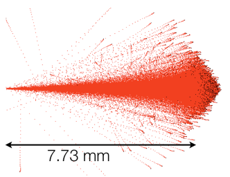
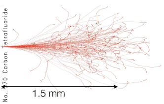
Because of the excellent spacial () and timing () resolution of the ATLAS pixel chip, we should be able to reconstruct relatively short tracks in three dimensions. Therefore, this type of detector should be effective for detecting neutral particles via the tracks produced in elastic scattering off the nuclei of the gas. These types of interactions can be used to detect particles such as neutrons or perhaps weakly interacting dark matter particles (WIMPs). Figure 1, shows nuclear recoils simulated with SRIM [5] for neutrons and WIMPs. The additional ability of the chip to measure the total charge should also enable us to determine the incoming direction of the particle.
One striking signature of dark matter would be the twelve hour directional oscillation of the WIMP recoils as the Earth rotates [6]. There is also interest to use such a detector to replace based neutron detectors used to detect nuclear material. Though not discussed here, similar TPCs are being proposed to study beam backgrounds at the Super KEKB accelerator in Japan.
2 Detector Prototypes
2.1 First Generation
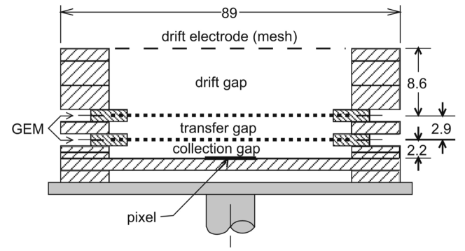
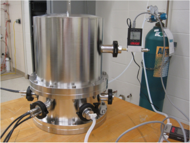
The construction of the first generation prototype was led by J. Kadyk at Lawrence Berkeley National Laboratory (LBNL) [2]. This prototype consists of a small drift gap with a drift electrode (consisting of a wire mesh) above and two layers of GEMs and the pixel chip below, Figure 2. This apparatus is contained within a vacuum vessel filled with a target gas. Several gases were studied (, , and ), and more work will be done to optimize the gas for WIMPs or neutrons, but the results shown are with in a ratio of 70/30 at 1 ATM.
2.1.1 ATLAS FE-I3 Pixel Chip
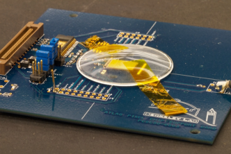
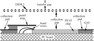
The ATLAS FE-I3 pixel chip (currently used in the ATLAS detector) was developed at LBNL over a 7 year period. It has an active area of 7.2 mm x 10.8 mm, with 2880 pixels of dimensions 50 x 400 arranged into 18 columns and 160 rows. The chip has very low noise, less than 120 electrons per pixel. The chip is self-triggering (with an adjustable trigger threshold) and has a readout integration time of 400 ns. In with a drift field 1 kV/cm, this equates to 10 mm.
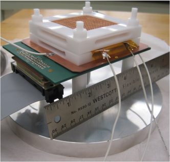
Because of the requirements of TPCs, some slight modifications of the standard ATLAS pixel chip test board, Figure 3a, are needed. The pixel sites on the FE-I3 chip were plated with either gold or aluminum to help maintain a uniform electric field and to help prevent surface charge from from building on the semiconductor. The board was redesigned to move the surface mounted readout electronics to the back of the board, and a copper collection pad and guard strip were also added, see Figure 3b.
2.1.2 Gas Electron Multipliers (GEM)
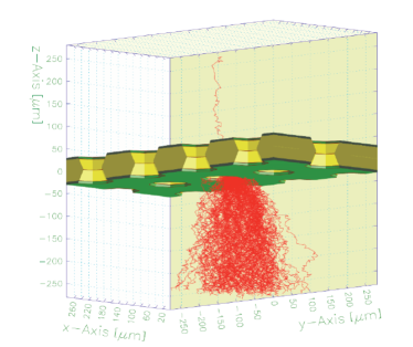
The GEMs, purchased from CERN, are 5 cm x 5 cm x 60 , and composed of a kapton layer between two thin sheets of copper. This structure is then chemically pierced with a hole spacing of 140 and 100% active area [8]. They reliably provide a gain of up to 300 in , however when operating the top GEM at 500 V and bottom GEM at 400 V we obtain a gain of 40000. Figure 4a shows a simulated avalanche of a single electron with a GEM bias of 500 V.
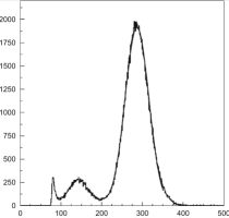
The gain of the GEMs is measured by placing an source in the vessel. The copper collection pad is used to collect the avalanche gain of the primary ionization from the source X-rays. This signal is recorded with a pulse height analyzer that was calibrated using a pulse generator. An example spectrum can be seen in Figure 4b. The primary peak corresponding to the 5.9 keV X-ray emission has a full-width-at-half-max (FWHM) of approximately 24%. The escape peak is also well resolved.
2.1.3 Cosmic Ray Data
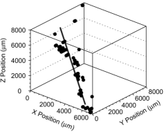
A large sample of cosmic ray events were collected with the LBNL prototype. Figure 5a shows one of these cosmic ray candidate track. For these events the drift field was set to 1 kV/cm, the gain was set to 9000, and the pixel threshold was set to 1800 electrons. Table 1 shows the x-z-y results for the cosmic ray sample.
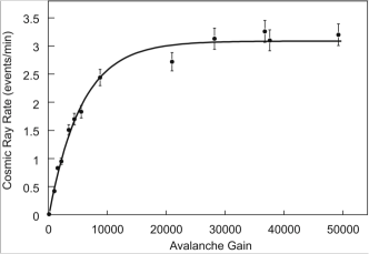
We then changed the pixel threshold and varied the GEM gain to test the detection efficiency with cosmic rays. Figure 5b shows the detection rate as a function of gain for a pixel threshold of 5000 electrons. The plot plateaus at a gain value consistent with a few times trigger threshold. This is consistent with all electrons being detected from the cosmic tracks.
| Fit Residual () | Diffusion () | () | |
| 170 | 110 | 130 | |
| 130 | 110 | 70 | |
| 240 | 190 | 150 |
2.1.4 University of Hawaii, Micro
2.2 Second Generation
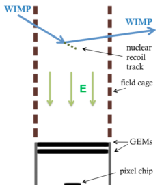
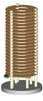
The Second Generation of the detector is a simple extension of the First Generation prototype. The main limitation of the first prototype is its small active volume, thus we simply remove the drift electrode and replace it with a 30 cm field cage, Figure 7a. Figure 7b, shows a computer aided design (CAD) [9] drawing of the proposed Second Generation prototype. During this phase of development we will begin to optimize the detector differently for dark matter searches () and for neutron detection (Directional Neutron Observer, DiNO).
3 Future Plans
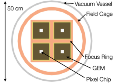
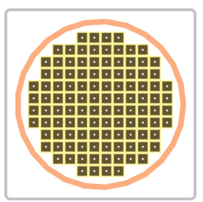
The ATLAS collaboration has continued the development of pixel chips for future upgrades. The next chip, FE-I4 [10], will be 2 cm x 2 cm. It will be paired with larger GEMs, 10 cm x 10 cm, enabling instrumentation of a larger volume. This will be implemented with the USBPIX readout developed at Bonn University [11]. This USB based readout system will further simplify the readout of multiple pixel chips. We are also working on a mechanism to focus the drifting electrons which will enable us to instrument a large volume at a lower cost. This work will be published elsewhere but is currently incorporated in the design of /DiNO.
With all (or even some) of these improvements, and a larger detector we may be able to detect dark matter. Figure 8 shows the proposed cellular design to be used in /DiNO, where each cell is similar to Figure 7a. Several layers, constructed as in Figure 8b, can be used to increase the active volume.
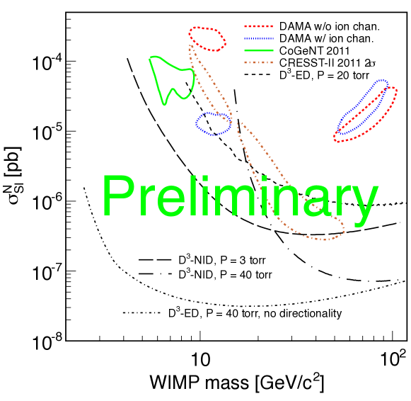
Figure 9, shows the expected limit for several different running scenarios. This plot includes a scenario where we use ion drift rather than electron drift [15]. This seems quite promising because of the reduction in diffusion, but we have not explored this experimentally yet. The electron drift (ED) limits and negative ion drift (NID) limits are calculated for and respectively. Both assume a one year of exposure to a detector with three of active volume constructed of nine layers, each with a 33.33 cm drift distance. This shows we may have sensitivity to areas of interest found by CRESST-II [12], DAMA/LIBRA [13], and CoGeNT [14]. While our ability to run at these low pressures have yet to be demonstrated, this study does suggest our possible discovery potential. Further information on our simulations can be found in [16].
4 Conclusions
While TPCs have been used for decades in high energy physics, we are developing a new variation that utilizes their strengths, large detector volume, and increases the precision and efficiency with the use of pixels and GEMs. The LBNL prototype has shown the detector design works well with cosmic rays. We have outlined a clear path to a larger detector, and have shown via simulation we may have sensitivity to discover or exclude a wide range of dark matter models.
Other projects, like the DMTPC collaboration [17], are using TPC for directional dark matter searches. We believe our use of the FE-I3 pixel chip will provide superior spacial and energy resolution. Since the TIPP conference, the University of Hawaii group has joined the DMTPC collaboration with hope of leveraging the expertise of both groups.
References
- [1] J. N. Marx, D. R. Nygren, The Time Projection Chamber, Phys.Today 31N10 (1978) 46. doi:10.1063/1.2994775.
- [2] T. Kim, M. Freytsis, J. Button-Shafer, J. Kadyk, S. Vahsen, et al., Readout of TPC tracking chambers with GEMs and pixel chip, Nucl.Instrum.Meth. A589 (2008) 173–184. doi:10.1016/j.nima.2008.02.049.
- [3] I. Peric, L. Blanquart, G. Comes, P. Denes, K. Einsweiler, et al., The FEI3 readout chip for the ATLAS pixel detector, Nucl.Instrum.Meth. A565 (2006) 178–187. doi:10.1016/j.nima.2006.05.032.
- [4] F. Sauli, GEM: A new concept for electron amplification in gas detectors, Nucl.Instrum.Meth. A386 (1997) 531–534. doi:10.1016/S0168-9002(96)01172-2.
- [5] M. D. Z. James F. Ziegler, Jochen P. Biersack, SRIM: The Stopping and Range of Ions in Matter, Lulu Press Co., 2009.
- [6] S. Ahlen, N. Afshordi, J. Battat, J. Billard, N. Bozorgnia, et al., The case for a directional dark matter detector and the status of current experimental efforts, Int.J.Mod.Phys. A25 (2010) 1–51. arXiv:0911.0323, doi:10.1142/S0217751X10048172.
- [7] R. Veenhof, GARFIELD, recent developments, Nucl.Instrum.Meth. A419 (1998) 726–730. doi:10.1016/S0168-9002(98)00851-1.
- [8] A. Bressan, J. Labbe, P. Pagano, L. Ropelewski, F. Sauli, Beam tests of the gas electron multiplier, Nucl.Instrum.Meth. A425 (1999) 262–276. doi:10.1016/S0168-9002(98)01406-5.
- [9] M.-S. K. G.E. Farin, J. Hoschek, Handbook of Computer Aided Geometric Design, NORTH-HOLLAND, 2002.
- [10] M. Garcia-Sciveres, D. Arutinov, M. Barbero, R. Beccherle, S. Dube, et al., The FE-I4 pixel readout integrated circuit, Nucl.Instrum.Meth. A636 (2011) S155–S159. doi:10.1016/j.nima.2010.04.101.
-
[11]
ATLAS and Bonn University,
USBpix
- USB based readout system for ATLAS FE-I3 and FE-I4 (July 2011).
URL http://icwiki.physik.uni-bonn.de/twiki/bin/view/Systems%/UsbPix - [12] G. Angloher, M. Bauer, I. Bavykina, A. Bento, C. Bucci, et al., Results from 730 kg days of the CRESST-II Dark Matter Search, arXiv:1109.0702.
- [13] R. Bernabei, P. Belli, F. Cappella, R. Cerulli, C. Dai, et al., New results from DAMA/LIBRA, Eur.Phys.J. C67 (2010) 39–49. arXiv:1002.1028, doi:10.1140/epjc/s10052-010-1303-9.
- [14] C. Aalseth, P. Barbeau, J. Colaresi, J. Collar, J. Leon, et al., Search for an Annual Modulation in a P-type Point Contact Germanium Dark Matter Detector, Phys.Rev.Lett. 107 (2011) 141301. arXiv:1106.0650.
- [15] C. J. Martoff, R. Ayad, M. Katz-Hyman, G. Bonvicini, A. Schreiner, Negative ion drift and diffusion in a TPC near 1 bar, Nuclear Instruments and Methods in Physics Research A 555 (2005) 55–58. arXiv:arXiv:physics/0406114, doi:10.1016/j.nima.2005.08.103.
- [16] I. Jaegle, et al., Simulation of the directional dark matter detector and directional neutron observer, CYGNUS 2011 Proceedings: EAS Pub. Series.
- [17] G. Sciolla, J. Battat, T. Caldwell, B. Cornell, D. Dujmic, et al., The DMTPC detector, PoS IDM2008 (2008) 002. arXiv:0811.2922.
