Cooling of photoexcited carriers in graphene by internal and substrate phonons
Abstract
We investigate the energy relaxation of hot carriers produced by photoexcitation of graphene through coupling to both intrinsic and remote (substrate) surface polar phonons using the Boltzmann equation approach. We find that the energy relaxation of hot photocarriers in graphene on commonly used polar substrates, under most conditions, is dominated by remote surface polar phonons. We also calculate key characteristics of the energy relaxation process, such as the transient cooling time and steady state carrier temperatures and photocarriers densities, which determine the thermoelectric and photovoltaic photoresponse, respectively. Substrate engineering can be a promising route to efficient optoelectronic devices driven by hot carrier dynamics.
I Introduction
Upon fast excitation of graphene carriers with light or other means, the dynamics of the resulting
non-equilibrium carrier distribution evolve on a fast time scale and has been extensively studied both experimentallySun et al. (2008); Dawlaty et al. (2008); Kampfrath et al. (2005); Breusing et al. (2009, 2011); Newson et al. (2009); Choi et al. (2009); Wang et al. (2010); George et al. (2008); Kumar et al. (2009); Ishioka et al. (2008); Seibert et al. (1990); Winnerl et al. (2011) and theoreticallyWinzer et al. (2010); Kim et al. (2011); Malic et al. (2011). The relaxation involves an initial fast evolution towards quasi-thermal distribution on a femtosecond timescale via electron-electron collisionsHertel and Moos (2000); Lui et al. (2010); Winzer et al. (2010); Kim et al. (2011), followed by energy transfer to phonons on a longer picosecond timescale.
The conversion of the excess energy of these photoexcited carriers
into electrical current before they lose this energy to the phonon baths represents one of the key challenges to
efficient optoelectronic device.
In this paper, we study the energy relaxation pathways of the
photoexcited carriers via different inelastic scattering channels.
Energy relaxation processes in graphene due to intrinsic optical and acoustic
phonons have already been studiedBistritzer and MacDonald (2009); Tse and Sarma (2009); Kubakaddi (2009); Kim et al. (2011). High energy optical phonon emission
by hot carriers is responsible for the subpicosecond fast cooling processSun et al. (2008); Dawlaty et al. (2008); Sun et al. (2012),
followed by cooling via the acoustic modes. The latter is a slow process, that creates
an electron-phonon cooling bottleneckBistritzer and MacDonald (2009).
Here, we focus on an extrinsic mechanism for cooling of photoexcited carriers in graphene
via the remote surface polar phonon modes (SPP) of the substrate and compare their efficiency
under different conditions with those of the internal phonon modes.
In polar substrates such as SiO2, a non-vanishing fluctuating electric field is generated by
the propagating surface phonon modesAshcroft and Mermin (1976).
The interactions of these SPP modes with charged carriers in the conduction channel
was first explored in the context of
inversion layer of semiconductor-oxide interfaceWang and Mahan (1972); Hess and Vogl (1979); Fischetti et al. (2001).
They have also been studied in other material systems such
as carbon nanotubesPetrov and Rotkin (2006); Perebeinos et al. (2009); Chandra et al. (2011),
where close proximity between charged carriers and
the underlying substrate renders the SPP-phonon scattering more prominent.
Similarly, in graphene, SPP was found to limit electronic transport propertiesMeric et al. (2008); Chen et al. (2008); Fratini and Guinea (2008); Perebeinos and Avouris (2010); Konar et al. (2010); Li et al. (2010); Price et al. (2012); Schiefele et al. (2012); Zou et al. (2010); Dasilva et al. (2010).
Recently, the SPP coupling with graphene plasmons
was also probed experimentally through infrared spectroscopyLiu and Willis (2010); Fei et al. (2011); Chen et al. (2012).
In this work, we found irrespectively of the mechanism i.e. thermoelectric or photovoltaic,
that SPP limits the overall strength of the steady state photoresponse on common substrates,
and our results suggest that elimination of the SPP cooling channel can lead to an order
of magnitude enhancement in the photoresponse.
In Sec. II, we present the general theory, where details of the models for the electron cooling power via the different phonon baths are presented in the Appendix. We present the results of our calculation of the cooling powers in Sec. III A and discuss their relative contribution in detail, as a function of doping and electronic/lattice temperatures. In Sec. III B, we apply the above models to the study of the cooling dynamics of hot carriers due to continuous or pulsed light excitations. We calculate key experimental observables such as the transient cooling time, and steady state quantities such as the non-equilibrium electronic temperatures, excess photocarriers density and the out-of-plane thermal conductivity for graphene on common substrates.
II Theory and Models
Transition probability for emission and absorption of phonons with a particular phonon bath is described by the Fermi’s golden rule,
| (1) |
where is the phonon momentum, is the Bose-Einstein distribution and are the transition matrix elements related to the coupling with phonon bath , to be defined below. For brevity, summation shall be implicit hereafter. The cooling power is computed numerically by accounting for the transfer of electronic energy to the lattice during each scattering event i.e. . Therefore the net cooling power is calculated viaConwell (1967); Manion et al. (1987); Bistritzer and MacDonald (2009); Kubakaddi (2009),
| (2) | |||||
where and are the lattice and electron temperatures respectively, and the electron distribution function is described by , and we define a composite Fermi-Boson distribution function as,
| (3) |
As indicated by experimentsSun et al. (2008); Dawlaty et al. (2008); Lui et al. (2010), the electronic system
is thermalized by the electron-electron interactions which occur at much
faster timescale than the electron-phonon processes we are calculating here.
Hence, it is appropriate to simply assume that
follows the Fermi Dirac distribution function, i.e.
where
and is the chemical potential, controlled by chemical doping
or electrical gating in experiments.
It is apparent that the composite electron-phonon distribution function
becomes zero when , hence zero cooling power.
In this work, we are interested in the energy exchange of electrons with the different phonon baths i.e. intrinsic acoustic phonons (AP), optical phonons (OP) and surface phonon polaritons (SPP). Vibrations of the substrate ions with the opposite charge polarity produce an electric field which decays exponentially away from the surface. Carriers in the nearby graphene can feel this electric field and be scattered by the SPP phonon. The decay length of the electric field is determined by the momentum transfer in the electron-phonon scattering event. For typical carrier density in graphene, the relevant momentum transfer is of the order of nm-1, such that a substantial coupling strength is expected for graphene placed at van der Waals distance of away from the substrate. The transition matrix elements, , for electron interaction with AP, OP and SPP phonons are well-known in the literaturesHwang and Sarma (2008); Lazzeri et al. (2005); Ando (2006a); Fratini and Guinea (2008); Fischetti et al. (2001); Perebeinos and Avouris (2010). We therefore defer their discussions to the Appendix, with the parameter set summarized in Table 1. We shall focus on the key results in what follows.
III Results and discussions
III.1 Competing cooling pathways
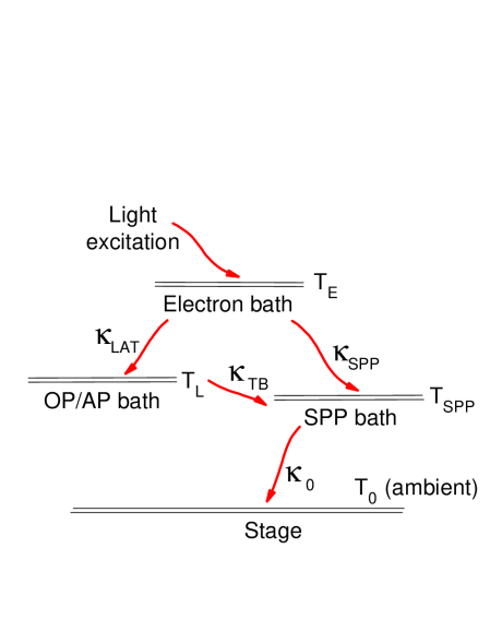
We begin with a simple illustration of the possible cooling pathways
for photoexcited carriers in graphene in Fig. 1.
Each thermal bath can be characterized by their respective temperatures ,
and are in general different from the ambient temperature .
The heat exchange between these thermal baths can
be described by the thermal conductivity, ,
defined as the ratio between the power exchange
per unit temperature difference i.e. .
In general, the different phonon baths can each establish a
different temperature upon interactions with the electrons (see also discussion in Sec. III.2).
In this work, we shall assume a common temperature for
all these phonon baths, denoted simply as the lattice temperature .
For a typical SiO2 substrate thickness of nm,
varies in a range MW/KmMW/Km2,
where SiO2 film thermal conductivity is W/mKYamane et al. (2002).
The interface thermal conductance of graphene on SiO2 substrate
has been measured using various experimental techniquesBalandin (2011); Chen et al. (2009); Freitag et al. (2009); Mak et al. (2010); Koh et al. (2010),
with values ranging from MW/KmMW/Km2.
On the theory front, several approaches have been employed
to estimate this interface thermal conductanceOng and Pop (2010); Persson and Ueba (2010a, b); Volokitin and Persson (2011); Petrov and Rotkin (2012),
which varies from MW/KmMW/Km2.
As illustrated in Fig. 1, energy transfered from
electrons to the internal phonon baths
is conducted to the underlying substrate
through a phonon-limited . between carbon surface
and SiO2 substrate has been estimated from molecular dynamics
and is MW/Km2Ong and Pop (2010), and can depend
also on the surface roughness.
Alternatively, energy can be transfered directly to the
substrate via the SPP phonons, i.e. ,
and can depend sensitively on doping.
For an undoped graphene, is on the order of MW/Km2
while is even smaller,
as we will see later in the discussion.
In this section, we discuss how these cooling pathways
depend on the various experimental conditions.
Detailed balance condition of in- and out-scattering processes requires that
vanishes under equilibrium condition i.e. .
In the theory, this is ensured by the composite Fermi-Boson distribution function .
The energy exchange efficiency with these various phonon baths depends upon, among other factors,
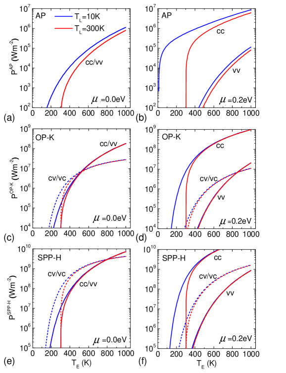
the doping and electronic/lattice temperatures. Using the models described in Sec. II,
we calculate due to the various phonon baths for intrinsic/doped graphene
under cold/hot (defined at K respectively) lattice temperature as shown in Fig. 2.
First, we discuss results on intrinsic graphene, see Fig. 2(a,c,e), which can be understood
on the basis of scattering phase space arguments.
For cold neutral graphene, Pauli blocking limits the electronic transitions involved to mainly interband processes.
Hence, under near equilibrium condition i.e. being small,
we observed that the cooling power is mainly dominated by interband processes by optical and SPP modes.
Increasing the electronic temperature alleviates Pauli blocking,
and allows for intraband processes to take place.
As increases further, we observe that intraband cooling begins to dominate over the interband counterpart.
The efficiency of energy exchange can be explained by
the electron-phonon occupation number, quantified by
the composite distribution function defined in Eq. 3. For inelastic processes,
one can show that is independent of when .
This is as reflected in Fig. 2 for and .
On the other hand, for quasi-elastic acoustic phonons, the cooling power is proportional instead.
The results on doped graphene are shown in Fig. 2(b,d,f).
Contrary to the intrinsic case, Pauli blocking promotes intraband electronic
transitions over interband processes in doped graphene.
In addition, ,
with larger cooling power for the majority carriers.
At moderate doping of eV, their cooling power
differs by more than an order of magnitude.
The reduced electron-hole symmetry upon doping also leads to smaller
interband cooling power.
Quasi-elasticity of acoustic phonon scattering results in
a phase space restriction in the scattering, with a Bloch-Grneisen temperature
determined by the dopingHwang and Sarma (2008); Efetov and Kim (2010), i.e. , in contrast to normal metals.
This increase in phase space in conjunction with Pauli blocking
greatly enhances the cooling power due to AP over the optical phonon baths.
In fact, for moderate K, dominates over all other mechanisms
for cold graphene.
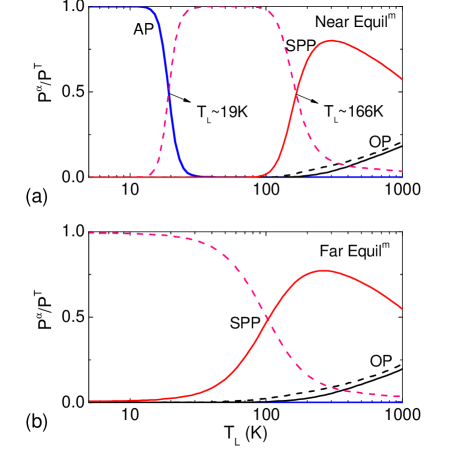
The lattice temperature, , also plays an important role in the
competing cooling pathways. Fig. 3 compares the fractional cooling powers / for intrinsic graphene,
where .
To obtain a quantitative estimate, we include in-plane screening of the SPP scattering potential in graphene.
The screening is incorporated through a standard procedureFerry and Goodnick (1997)
.
For simplicity, we employed the static screening dielectric function , which
in the long-wavelength limit assumes a simple formAndo (2006b) ,
where =
and is graphene density-of-states. is the Fermi distribution function
and is a function of the electronic temperature.
We analyze the results in two non-equilibrium temperature limits, namely “near equilibrium” (K) and “far from equilibrium” (K) conditions. Fig. 3a considers the condition of “near equilibrium”. At low , AP dominates cooling. Increasing populates the low-energy SPP mode, which begins to overtake the cooling power at a temperature of K. This transition temperature increases with doping e.g. is K at a doping of eV. The low energy SPP mode is overtaken by its high-energy mode at K. A downturn in the high-energy SPP cooling power is observed, due to larger screening at higher temperatures. Eventually, the optical phonons overtake the SPP for temperatures larger than K. Fig. 3b considers the condition of “far from equilibrium”. In this case, the SPP dominates the cooling power for all , except at temperature K where optical phonons begin to overtake it.
III.2 Cooling dynamics
We are interested in the role played by these various phonon baths on the cooling dynamics of photoexcited carriers,
more specifically, the temporal evolution of .
The acoustic and optical phonon baths can each establish a
different temperature upon interactions with the electrons, but processes such as
anharmonic phonon-phonon scattering serve to thermalize them on a picosecond time scaleKampfrath et al. (2005); Bonini et al. (2007); Song et al. (2008); Yan et al. (2009).
In this work, we shall assume a common lattice temperature ,
but acknowledge that in experiments with ultrafast pump-probe, this will not hold true.
On the other hand, under continuous light excitation, coupling to the heat sink
via the supporting substrate substantially cools the lattice
temperature to within a few degrees Kelvin of the ambient temperature
under usual photoexcitation conditionsFreitag et al. (2012).
Typically, under low/moderate excitation power levels used in our studies.
In this regard, the relatively small differences among the various phonon baths can be safely ignored.
Hot carriers dynamics can be probed through optical measurementsShah (1992); Sun et al. (2008); Dawlaty et al. (2008); Kampfrath et al. (2005). Following a pulsed light excitation, the temporal evolution of carrier relaxation, quantified by its electronic temperature , can be measured using differential transmission spectroscopy. The electron dynamics are usually described by , and can be estimated withSong et al. (2011a),
| (4) |
where is the electron specific heat
and is the energy density of graphene.
In this work, is computed numerically. However, we note that
for , increases linearly with , i.e.
.
Having computed the total cooling power in Sec. III,
can be obtained directly from Eq. 4.
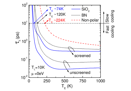
Fig. 4 plots the cooling time, , for neutral graphene at K.
It is calculated for common substrates such as SiO2, BN and non-polar substrate
such as diamond. At very hot electron temperatures, i.e. K,
is given by a relatively constant sub-picosecond
cooling time.
This is in agreement with experimentsSun et al. (2012).
The constancy of suggests the decay
characteristics typical during the initial fast cooling process.
As cools down, the cooling bottleneck due to AP begins to set in,
leading to much slower cooling times.
The transition temperature into this slow cooling regime varies
with the choice of substrate as indicated in Fig. 4.
This transition temperature is dictated by the lowest
frequency SPP mode of the substrate.
Unscreened results, which overestimate the SPP cooling power, yield much
shorter cooling lifetimes than experimentally reportedSun et al. (2012).
We also note that inclusion of disorder assisted coolingSong et al. (2011a),
might enhance the decay rate, especially in the slow cooling regime.
The optoelectronic response in graphene, photovoltaicXia et al. (2009); Lee et al. (2008); Park et al. (2009)
or thermoelectricGabor et al. (2011); Xu et al. (2009); Sun et al. (2012), is also a measure of the
energy transport of these hot carriers.
These experiments are usually performed under a continuous light
illumination of an electrostatic junction.
Their relative contribution depends on the electrostatic junction characteristics,
doping, and even extrinsic factors such as electron-hole puddlesSong et al. (2011b).
Nevertheless, at steady state, the photovoltaic current is proportional to the
photo-generated excess carrier density, , via
where is the carrier mobility and the local electric field.
The thermoelectric response, on the other hand, is proportional to the
local elevated temperature, =, via
where is the Seebeck coefficient of the two junction
and is the device conductivity.
Here, we discuss estimates of and .
Under steady state condition,
| (5) |
where is the laser power absorbed by graphene, and
is the heat dissipation via the metallic contacts, if any.
In the absence of contacts, all heat dissipation is
via the supporting substrate. At steady state,
.
Eq. 5 is then solved self-consistently
in conjunction with charge conservation i.e.
=, arriving at steady state values for and .
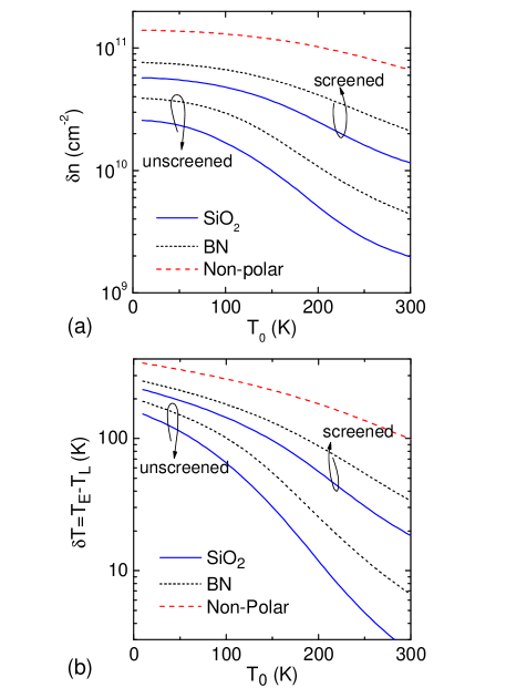
The photoexcited carrier density, , and the elevated temperature,
are plotted in Fig. 5(a-b) respectively,
assuming typical experimental values of W/m2 and
MW/Km2.
Both and decrease with increasing ambient temperature ,
due to more efficient cooling as phonon occupation increases.
For SiO2, cm-2 and K
under room temperature condition, of the same order typically seen in measurementFreitag et al. (2012).
Increasing doping increases the scattering phase space for intraband processes and lead to
more efficient electronic cooling into the phonon baths, as shown
in Fig. 2. As a result, both and
decrease with increasing doping.
We also estimate the heat dissipation via contacts phenomenologically with
where is
the distribution function before light excitation.
First, we consider the simple ballistic limit where is just the
device lifetime given by , where is the length of the device and m/s is the Fermi velocity.
Here, we assume a typical ps. We found that including only
leads to few-fold decrease in the quantitative results presented in Fig. 5 (not shown).
In the realistic case where the carrier transport is in the diffusive
dominated regime, would be even smaller, by a factor
of , where is the carrier’s mean free path.
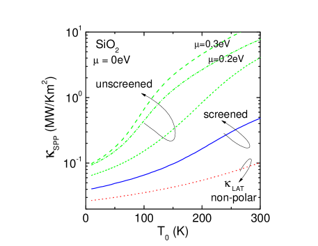
Fig. 5 also suggests an order of magnitude enhancement in the optoelectronic response of graphene, by suppressing the SPP heat dissipation through a non-polar substrate, such as diamond-like carbonWu et al. (2011), or by suspending graphene. In fact, the amount of heat transfer to the substrate via the electron coupling with the SPP can be quantified by an out-of-plane thermal conductance , defined as . This quantity sets the lower limit on the interfacial thermal conductance and it is plotted in Fig. 6. At room temperature, MW/Km2 for undoped graphene, and can increases with doping to order of MW/Km2, see also Ref. Petrov and Rotkin (2012). For typical photocurrent experiments, is typically , and transport is in the diffusive regime. Here, the in-plane electronic thermal conductivity, , can be estimated from the Wiedemann Franz relation. We found that our estimated value of is significantly larger than for typical experimental situations. This suggests that out-of-plane heat dissipation via SPP dominates over the in-plane electronic heat conduction. The former leads to an increased temperature of the graphene lattice. This result reconciles with recent experimentFreitag et al. (2012), which reveals significant lattice heating upon laser excitation. From the experimentFreitag et al. (2012), we can estimate an out-of-plane thermal conductance of MW/Km2. This value is consistent with our estimated . In fact, alone is orders of magnitude smaller than the experiment as shown in Fig. 6.
IV Conclusions
Our results point to the limiting role played by remote substrate phonons in the energy relaxation of hot
photocarriers. In particular, we have shown that the steady state photoresponse in graphene is controlled by the inelastic scattering. The photovoltaic current is proportional to the photo-generated excess carrier density. The thermoelectric contribution, on the other hand, is proportional to the elevated electron temperature. Our results show that irrespective of the mechanism, the SPP phonons limits the overall strength of the photocurrent response on polar substrates. We predict that a choice of a non-polar substrate will lead to an order of magnitude enhancement in graphene photoresponse. Therefore, substrate engineering presents a promising route to efficient optoelectronic devices driven by hot carrier dynamics.
Acknowledgements: TL acknowledges use of a computing cluster provided by Network for Computational Nanotechnology, partial funding from INDEX-NRI and in part by the NSF under Grant No. NSF PHY05-51164 (KITP). We thank F. Xia, H. Yan, F. Guinea, E. Hwang and X. Xu for useful discussions.
Appendix A Acoustic phonon
We consider first the energy exchange with the acoustic phonon (AP) bath. The total matrix element for electron-acoustic phonon scattering due to the two acoustic phonon modes, i.e. and , is given byHwang and Sarma (2008); Perebeinos and Avouris (2010),
| (6) |
where is the acoustic deformation potential, taken to be eV in our calulations, which is very
similar to the recent ab-initio calculations of eVKaasbjerg et al. (2012).
We note that the electron-phonon matrix element for these two acoustic modes have
different angular dependencies with transition matrix elementsPietronero et al. (1980); Kaasbjerg et al. (2012),
which became negated after summing themPietronero et al. (1980).
is graphene effective sound velocity defined asPerebeinos and Avouris (2010) ,
where km/s, km/s and km/s.
is graphene mass density taken to be kg/m2.
The acoustic phonon is then described by an effective Debye linear dispersion .
Since , is typically much smaller than other energy scale in the problem.
The acoustic phonon scattering is thus approximated to be elasticBistritzer and MacDonald (2009) i.e. .
The cooling power can then be written as,
| (7) | |||||
Under the assumption , we have
| (8) |
Making use of the relations , we then obtain a simplified form for the cooling power,
| (9) |
Contributions from interband processes, , are forbidden due to energy-momentum conservations.
Appendix B Optical phonons
Next, we discuss energy exchanges with high energy dispersionless optical phonon (OP) modes i.e. , and . We consider first the electron-phonon coupling of long-wavelength optical phonon modes, and . Their sum is expressed asLazzeri et al. (2005); Ando (2006a),
| (10) |
where eV is the
optical-phonon deformation potential with a coupling constant of eV,
and meV.
We note that the electron-phonon matrix element for these two optical modes have
different angular dependencies with transition matrix elementsLazzeri et al. (2005); Ando (2006a)
i.e. where denotes conduction/valence bands,
which again became negated after summing them.
We consider first the intraband cooling power, written as,
| (11) | |||||
In similar fashion, the interband cooling power is written as,
| (12) |
where is the Heaviside function.
For zone edge phonon modes, only the transverse contributes to carrier scattering, and the matrix element isLazzeri et al. (2005),
| (13) |
where eV and meV. The cooling power is similar to the phonons case, except a factor of smaller due to the angular dependence.
Appendix C Surface polar phonons
The surface polar phonons coupling is given byFratini and Guinea (2008); Fischetti et al. (2001); Perebeinos and Avouris (2010),
| (14) |
where is the free space permittivity and is the separation between
graphene and the substrate. The magnitude of the polarization field
is given by the Frohlich coupling parameter, .
In common SiO2 dielectrics, there are two dominant surface optical phonon modes
having energies meV and meV,
with Frohlich coupling meV and meV respectivelyPerebeinos and Avouris (2010).
We consider first the intraband cooling power, written as,
| (15) | |||||
The phonon momentum has the constraint . Under typical conditions, the factor . Linearizing , the intraband cooling power then becomes,
| (16) |
where and
| (17) | |||||
where are the complete elliptic integrals of first and second kind. In similar fashion, the interband cooling power is written as,
| (18) | |||||
where .
References
- Sun et al. (2008) D. Sun, Z. K. Wu, C. Divin, X. Li, C. Berger, W. A. de Heer, P. N. First, and T. B. Norris, Phys. Rev. Lett. 101, 157402 (2008).
- Dawlaty et al. (2008) J. M. Dawlaty, S. Shivaraman, M. Chandrashekhar, F. Rana, and M. G. Spencer, Appl. Phys. Lett. 92, 042116 (2008).
- Kampfrath et al. (2005) T. Kampfrath, L. Perfetti, F. Schapper, C. Frischkorn, and M. Wolf, Phys. Rev. Lett. 95, 187403 (2005).
- Breusing et al. (2009) M. Breusing, C. Ropers, and T. Elsaesser, Phys. Rev. Lett. 102, 086809 (2009).
- Breusing et al. (2011) M. Breusing, S. Kuehn, T. Winzer, E. Malic, F. Milde, N. Severin, J. P. Rabe, A. Knorr, and T. Elsaesser, Phys. Rev. B 83, 153410 (2011).
- Newson et al. (2009) R. W. Newson, J. Dean, B. Schmidt, and H. M. van Driel, Opt. Exp. 17, 2326 (2009).
- Choi et al. (2009) H. Choi, F. Borondics, D. A. Siegel, S. Y. Zhou, M. C. Martin, A. Lanzara, and R. A. Kaindl, Appl. Phys. Lett. 94, 172102 (2009).
- Wang et al. (2010) H. Wang, J. H. Strait, P. A. George, S. Shivaraman, V. B. Shields, M. Chandrashekhar, J. Hwang, F. Rana, M. G. Spencer, C. S. Ruiz-Vargas, et al., Appl. Phys. Lett. 96, 081917 (2010).
- George et al. (2008) P. A. George, J. Strait, J. Dawlaty, S. Shivaraman, M. Chandrashekhar, F. Rana, and M. G. Spencer, Nano Lett. 8, 4248 (2008).
- Kumar et al. (2009) S. Kumar, M. Anija, N. Kamaraju, K. S. Vasu, K. S. Subrahmanyam, A. K. Sood, and C. N. R. Rao, Appl. Phys. Lett. 95, 191911 (2009).
- Ishioka et al. (2008) K. Ishioka, M. Hase, M. Kitajima, L. Wirtz, A. Rubio, and H. Petek, Phys. Rev. B 77, 121402 (2008).
- Seibert et al. (1990) K. Seibert, G. C. Cho, W. Kütt, H. Kurz, D. H. Reitze, J. I. Dadap, H. Ahn, M. C. Downer, and A. M. Malvezzi, Phys. Rev. B 42, 2842 (1990).
- Winnerl et al. (2011) S. Winnerl, M. Orlita, P. Plochocka, P. Kossacki, M. Potemski, T. Winzer, E. Malic, A. Knorr, M. Sprinkle, C. Berger, et al., Phys. Rev. Lett. 107, 237401 (2011).
- Winzer et al. (2010) T. Winzer, A. Knorr, and E. Malic, Nano Lett. 10, 4839 (2010).
- Kim et al. (2011) R. Kim, V. Perebeinos, and P. Avouris, Phys. Rev. B 84, 075449 (2011).
- Malic et al. (2011) E. Malic, T. Winzer, E. Bobkin, and A. Knorr, Phys. Rev. B 84, 205406 (2011).
- Hertel and Moos (2000) T. Hertel and G. Moos, Phys. Rev. Lett. 84, 5002 (2000).
- Lui et al. (2010) C. H. Lui, K. F. Mak, J. Shan, and T. F. Heinz, Phys. Rev. Lett. 105, 127404 (2010).
- Bistritzer and MacDonald (2009) R. Bistritzer and A. H. MacDonald, Phys. Rev. Lett. 102, 206410 (2009).
- Tse and Sarma (2009) W. K. Tse and S. D. Sarma, Phys. Rev. B 79, 235406 (2009).
- Kubakaddi (2009) S. S. Kubakaddi, Phys. Rev. B 79, 075417 (2009).
- Sun et al. (2012) D. Sun, G. Aivazian, A. M. Jones, J. S. Ross, W. Yao, D. Cobden, and X. Xu, Nat. Nano. 7, 114 (2012).
- Ashcroft and Mermin (1976) N. W. Ashcroft and D. N. Mermin, Solid State Physics (Harcourt Brace College, New York) p. 27 (1976).
- Wang and Mahan (1972) S. Q. Wang and G. D. Mahan, Phys. Rev. B 6, 4517 (1972).
- Hess and Vogl (1979) K. Hess and P. Vogl, Solid State Comm. 30, 807 (1979).
- Fischetti et al. (2001) M. V. Fischetti, D. A. Neumayer, and E. A. Cartier, J. Appl. Phys. 90, 4587 (2001).
- Petrov and Rotkin (2006) A. G. Petrov and S. V. Rotkin, JETP Lett. 84, 156 (2006).
- Perebeinos et al. (2009) V. Perebeinos, S. V. Rotkin, A. G. Petrov, and P. Avouris, Nano Lett. 9, 312 (2009).
- Chandra et al. (2011) B. Chandra, V. Perebeinos, S. Berciaud, J. Katoch, M. Ishigami, P. Kim, T. F. Heinz, and J. Hone, Phys. Rev. Lett. 107, 146601 (2011).
- Meric et al. (2008) I. Meric, M. Y. Han, A. F. Young, B. Ozyilmaz, P. Kim, and K. L. Shepard, Nature Nano 3, 654 (2008).
- Chen et al. (2008) J. H. Chen, C. Jang, S. Xiao, M. Ishigami, and M. S. Fuhrer, Nature Nano 3, 206 (2008).
- Fratini and Guinea (2008) S. Fratini and F. Guinea, Phys. Rev. B 77, 195415 (2008).
- Perebeinos and Avouris (2010) V. Perebeinos and P. Avouris, Phys. Rev. B 81, 195442 (2010).
- Konar et al. (2010) A. Konar, T. Fang, and D. Jena, Phys. Rev. B 82, 115452 (2010).
- Li et al. (2010) X. Li, E. A. Barry, J. M. Zavada, M. B. Nardelli, and K. W. Kim, Appl. Phys. Lett. 97, 232105 (2010).
- Price et al. (2012) A. S. Price, S. M. Hornett, A. V. Shytov, E. Hendry, and D. W. Horsell, arXiv: 1202.3394 (unpublished) (2012).
- Schiefele et al. (2012) J. Schiefele, F. Sols, and F. Guinea, arXiv: 1202.2440 (unpublished) (2012).
- Zou et al. (2010) K. Zou, X. Hong, D. Keefer, and J. Zhu, Phys. Rev. Lett. 105, 126601 (2010).
- Dasilva et al. (2010) A. M. Dasilva, K. Zou, J. K. Jain, and J. Zhu, Phys. Rev. Lett. 104, 236601 (2010).
- Liu and Willis (2010) Y. Liu and R. F. Willis, Phys. Rev. B 81, 081406 (2010).
- Fei et al. (2011) Z. Fei, G. O. Andreev, W. Bao, L. M. Zhang, A. S. McLeod, C. Wang, M. K. Stewart, Z. Zhao, G. Dominguez, M. Thiemens, et al., Nano Lett. 11, 4701 (2011).
- Chen et al. (2012) J. Chen, M. Badioli, P. A. Gonzalez, S. Thongrattanasiri, F. Huth, J. Osmond, M. Spasenovic, A. Centeno, A. Pesquera, P. Godignon, et al., arxiv: 1202.4996 (2012).
- Conwell (1967) E. M. Conwell, Solid State Physics Supplement (Academic, New York) (1967).
- Manion et al. (1987) S. J. Manion, M. Artaki, M. A. Emanuel, J. J. Coleman, and K. Hess, Phys. Rev. B 35, 9203 (1987).
- Hwang and Sarma (2008) E. H. Hwang and S. D. Sarma, Phys. Rev. B 77, 115449 (2008).
- Lazzeri et al. (2005) M. Lazzeri, S. Piscanec, F. Mauri, A. C. Ferrari, and J. Robertson, Phys. Rev. Lett. 95, 236802 (2005).
- Ando (2006a) T. Ando, J. Phys. Soc. Jpn. 75, 124701 (2006a).
- Geick et al. (1966) R. Geick, C. H. Perry, and G. Rupprecht, Phys. Rev. 146, 543 (1966).
- Yamane et al. (2002) T. Yamane, N. Nagai, S. Katayama, and M. Todoki, J. Appl. Phys. 91, 9772 (2002).
- Balandin (2011) A. A. Balandin, Nature Mat. 10, 569 (2011).
- Chen et al. (2009) Z. Chen, W. Jang, W. Bao, C. N. Lau, and C. Dames, Appl. Phys. Lett. 95, 161910 (2009).
- Freitag et al. (2009) M. Freitag, M. Steiner, Y. Martin, V. Perebeinos, Z. Chen, J. C. Tsang, and P. Avouris, Nano Lett. 9, 1883 (2009).
- Mak et al. (2010) K. F. Mak, C. H. Lui, and T. F. Heinz, Appl. Phys. Lett. 97, 221904 (2010).
- Koh et al. (2010) Y. K. Koh, M.-H. Bae, D. G. Cahill, and E. Pop, Nano Lett. 10, 4363 (2010).
- Ong and Pop (2010) Z.-Y. Ong and E. Pop, Phys. Rev. B 81, 155408 (2010).
- Persson and Ueba (2010a) B. N. J. Persson and H. Ueba, Euro. Phys. Lett. 91, 56001 (2010a).
- Persson and Ueba (2010b) B. N. J. Persson and H. Ueba, J. Phys. C. 22, 462201 (2010b).
- Volokitin and Persson (2011) A. I. Volokitin and B. N. J. Persson, Phys. Rev. B 83, 241407 (2011).
- Petrov and Rotkin (2012) A. G. Petrov and S. V. Rotkin, to be published (2012).
- Efetov and Kim (2010) D. K. Efetov and P. Kim, Phys. Rev. Lett. 105, 256805 (2010).
- Ferry and Goodnick (1997) D. K. Ferry and S. M. Goodnick, Transport in nanostructures, Cambridge University Press (1997).
- Ando (2006b) T. Ando, J. Phys. Soc. Jpn 75, 074716 (2006b).
- Bonini et al. (2007) N. Bonini, M. Lazzeri, N. Marzari, and F. Mauri, Phys. Rev. Lett. 99, 176802 (2007).
- Song et al. (2008) D. Song, F. Wang, G. Dukovic, M. Zheng, E. D. Semke, L. E. Brus, and T. F. Heinz, Phys. Rev. Lett. 100, 225503 (2008).
- Yan et al. (2009) H. Yan, D. Song, K. F. Mak, I. Chatzakis, J. Maultzsch, and T. F. Heinz, Phys. Rev. B 80, 121403(R) (2009).
- Freitag et al. (2012) M. Freitag, T. Low, F. Xia, and P. Avouris, arxiv: 1202.5342 (unpublished) (2012).
- Shah (1992) J. Shah, Hot carrier in semiconductor nanostructures, Academic London (1992).
- Song et al. (2011a) J. C. W. Song, M. Y. Reizer, and L. S. Levitov, arXiv: 1111.4678v1 (unpublished) (2011a).
- Xia et al. (2009) F. Xia, T. Mueller, Y. M. Lin, A. V. Garcia, and P. Avouris, Nat. Nano. 4, 839 (2009).
- Lee et al. (2008) E. J. Lee, K. Balasubramanian, R. T. Weitz, M. Burghard, and K. Kern, Nat. Nano. 3, 486 (2008).
- Park et al. (2009) J. Park, Y. H. Ahn, and C. Ruiz-Vargas, Nano. Lett. 9, 1742 (2009).
- Gabor et al. (2011) N. M. Gabor, J. C. W. Song, Q. Ma, N. L. Nair, T. Taychatanapat, K. Watanabe, T. Taniguchi, L. S. Levitov, and P. Jarillo-Herroro, Science 334, 648 (2011).
- Xu et al. (2009) X. Xu, N. M. Gabor, J. S. Alden, A. M. va der Zande, and P. L. McEuen, Nano Lett. 10, 562 (2009).
- Song et al. (2011b) J. C. W. Song, M. S. Rudner, C. M. Marcus, and L. S. Levitov, Nano Lett. 11, 4688 (2011b).
- Wu et al. (2011) Y. Wu, Y. M. Lin, A. A. Bol, K. A. Jenkins, F. Xia, D. B. Farmer, Y. Zhu, and P. Avouris, Nature 472, 74 (2011).
- Kaasbjerg et al. (2012) K. Kaasbjerg, K. S. Thygesen, and K. W. Jacobsen, Phys. Rev. B 85, 165440 (2012).
- Pietronero et al. (1980) L. Pietronero, S. Strassler, H. R. Zeller, and M. J. Rice, Phys. Rev. B 22, 904 (1980).