Nonlocal transport near the charge neutrality point in a two-dimensional electron-hole system
Abstract
Nonlocal resistance is studied in a two-dimensional system with a simultaneous presence of electrons and holes in a 20 nm HgTe quantum well. A large nonlocal electric response is found near the charge neutrality point (CNP) in the presence of a perpendicular magnetic field. We attribute the observed nonlocality to the edge state transport via counter propagating chiral modes similar to the quantum spin Hall effect at zero magnetic field and graphene near Landau filling factor .
pacs:
71.30.+h, 73.40.QvTopological insulators have an insulating gapped phase in the bulk and conducting edge modes, which propagate along the sample periphery kane ; bernevig ; hasan ; qi ; konig ; buhmann . All two-dimensional topological insulators (2DTI) can be divided into two classes: the integer quantum Hall effect (QHE) state prange and the quantum spin Hall effect (QSHE) state hasan , where the transport is described by the chiral/helical edge modes in the presence/absence of magnetic field B respectively. The chiral modes in QHE are robust to disorder due to magnetic field induced time reversal (TR) symmetry breaking halperin and propagate over macroscopic distances. A single pair of helical edge states in quantum spin Hall effect with an opposite spin polarization is also expected to be robust to nonmagnetic disorder due to preservation of TR symmetry maciejko . The quantum Hall effect state can be realized in any 2D metal in a strong perpendicular magnetic field, while the quantum spin Hall state exists in 2D systems with strong spin orbit interaction at B=0. The QSH state was first discovered in HgTe/CdTe quantum wells konig ; buhmann .

An unambiguous way to prove the presence of edge state transport mechanism in a 2DTI are the nonlocal electrical measurements. The application of the current between a pair of the probes creates a net current along the sample edge, and can be detected by another pair of the voltage probes away from the dissipative bulk current path. Note that the physics of the nonlocality in the QHE regime and in the QSHE systems is different. Figure 1 illustrates various transport mechanisms realized in different 2DTIs. In the QHE regime the nonlocal resistance arises from the suppression of electron scattering between the outermost edge channels and backscattering of the innermost channel via the bulk states buttiker ; mcEuen ; dolgopolov . It may occur only when the topmost Landau level (LL) is partially occupied i.e at , and the scattering via bulk states is allowed. The transport measurements roth ; gusev2 in HgTe quantum wells at B=0 reported unique nonlocal conduction properties due to the helical edge states.
It is worth noting that transport properties of HgTe quantum wells depend strongly on the well width. As the quantum well width becomes slightly larger than the ”critical” width, approximately equal to 6.3 nm, the energy spectrum becomes inverted and one gets a quantum spin Hall insulator. For still higher values of the well width the quantum well energy spectrum experiences further transformation. A calculation of the energy spectrum of a wide 20 nm HgTe QW, has been performed in Ref.[19] taking into account the strain caused by HgTe/CdTe lattice mismatch. It has been found that the strain leads to a small overlap of the conductance and valence band resulting in the formation of a semimetal. The strained 20nm HgTe QW is the semimetal with the zero gap so it does not have the quantum spin-Hall effect in contrast to 8nm HgTe samples. The transport in such a bipolar system at the charge neutrality point and in a strong magnetic field is in many respects qualitatively similar to the quantum Hall effect in graphene. For example, the resistance was found to increase very strongly with B while the Hall resistivity turns to zero gusev . We attributed the observed resistance growth to a percolation of the snake-type trajectories.
In this Letter we present an experimental study of the nonlocal resistance in a 2D bipolar system in undoped 20 nm wide HgTe quantum wells with an inverse band structure and (001) olshanetsky surface orientations. We find the nonlocal resistance increasing significantly with magnetic field near the charge neutrality point. We explain the observed large nonlocal resistance using the transport model with counter propagating chiral edge modes similar to the QSHE at B=0 and graphene at .

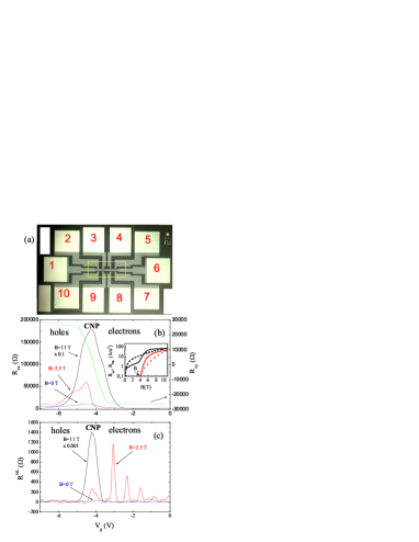
The quantum wells with the (001) surface orientations and the width of 20 nm were prepared by molecular beam epitaxy. A detailed description of the sample structure has been given in kvon ; gusev ; olshanetsky . The top view of a typical experimental sample is shown in Figure 2a. The sample consists of three wide consecutive segments of different length (), and 8 voltage probes. The ohmic contacts to the two-dimensional gas were formed by the in-burning of indium. To prepare the gate, a dielectric layer containing 100 nm and 200 nm was first grown on the structure using the plasmochemical method. Then, the TiAu gate was deposited. The density variation with gate voltage was . The magnetotransport measurements in the described structures were performed in the temperature range 1.4-70 K and in magnetic fields up to 11 T using a standard four point circuit with a 3-13 Hz ac current of 1-10 nA through the sample, which is sufficiently low to avoid the overheating effects. Several devices from the same wafer have been studied.
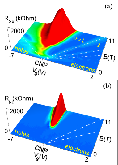
Figures 2b and c show the results obtained in the representative sample. Sweeping the gate voltage from 0 to negative values will depopulate the electron states and populate the hole states. At there is a coexistence of electrons and holes with close densities. The density of the carriers at the CNP without magnetic field was , the corresponding mobility was for electrons and holes. These parameters were found from comparison of the Hall and the longitudinal magnetoresistance traces with the Drude theory for transport in the presence of two types of carriers kvon ; olshanetsky . The local resistance peak corresponding to the CNP increases to 1800 at 11 T, whereas the peaks corresponding to higher Landau levels remain below 10 . Surprisingly, the nonlocal resistance measured in configuration (I=3,9;V=4,8), i.e. where the current flows between contacts 3,9 and the voltage is measured between contacts 4 and 8 in Figure 2 a, grows from zero at B=0 to 1400 a B=11 T and becomes comparable with the local resistance at the CNP. The peaks in on the electron side of the CNP in Figure 2 c remain practically the same up to B=11 T and can be attributed to the well known nonlocality of the quantum Hall effect edge state transport mcEuen ; dolgopolov . We don’t see such peaks on the hole side, because the hole mobility is much smaller than electron mobility. Insert to Fig.2b shows and at the CNP as a function of the magnetic field. We can see that the nonlocal magnetoresisance is strongly enhanced above the critical magnetic field . Figure 3 shows the local (a) and nonlocal (b) resistance in the voltage-magnetic field plane. One can see the evolution of both resistances with magnetic field and density close to the CNP. Nonlocal resistance has a comparable amplitude, similar peak position, but a narrower width.
The classical ohmic contribution to the nonlocal effect is given by for narrow strip geometry where L is the distance between the voltage probes, and is the strip width pauw . For our geometry we estimate for both zero and nonzero magnetic field. Therefore we can exclude the classical explanation of the observed nonlocality at finite B while it can possibly account for the absence of a noticeable nonlocality at B=0. We have measured the nonlocal response in other geometries, for example, (I=3,9;V=5,6), and found that the signal is almost independent of the contact configuration.
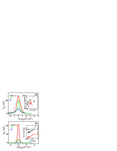
We have also examined the local and nonlocal responses near the CNP as a function of temperature with B fixed at 11 T (Fig.4 a,b). We see that both resistances increase with the temperature decreasing. We find that the profile of the and temperature dependencies does not fit the activation law , where is the activation gap (insert to Figure 4a), below . A similar behaviour has been reported in our previous study for the local response in the QHE regime at Landau filling factor near the charge neutrality point in samples with (013) surface orientation gusev . Note, however, that the nonlocal resistance is found to be more sensitive to temperature than the local resistance: the peak in disappears completely above 60 K.
Generally a nonlocal response occurs naturally in a 2D system with the edge state transport. For example in the integer quantum Hall state all current is carried by the chiral edge states, while electrons in the bulk region are localized. Note that the bulk conductivity is shunted by the edge transport and therefore . This agrees well with our observation of the nonlocal resistance peaks values in the quantum Hall effect regime on the electron side of the CNP (figure 2 c) but disagrees with the behaviour of the nonlocal resistance near the CNP.

Another example of the edge state transport is the 2D topological insulator. Our samples have a wider width of 20 nm and demonstrate properties of the semimetal rather than topological insulator. The zero magnetic field behavior of our 20 nm QWs differs from that of 8 nm wide HgTe quantum wells: the 2DTI in an 8 nm QW shows a large nonlocality, while in the 2D semimetal the nonlocal response is zero (figure 2c). Application of magnetic field induces a transition from the helical to the chiral edge states and so suppresses nonlocality in the 2DTI gusev2 . In the 2D semimetal, on the contrary, magnetic field may result in an opposite effect - an enhancement of the nonlocal resistance due to the edge state contribution to transport.

In the rest of the Letter we will focus on the explanation of the giant nonlocal magnetoresistance observed in our 20 nm wide HgTe quantum wells with 2D semimetal.
The transport in a 2D semimetals in a strong magnetic field is equivalent to the QHE state near the CNP in graphene within a spin-first splitting scenario abanin1 . The magnetic field creates a pair of gapless counter propagating edge states. The sharp peak in the local and nonlocal resistivities near CNP with a coexistence of electrons and holes can be explained in terms of a model including simultaneously the edge states and bulk transport and taking into account the backscattering both between the edge states (described by one single phenomenological parameter ) and a bulk-edge state coupling (described by a phenomenological parameter ).
Fig.4 shows the modeled behaviour of the local and nonlocal resistance as a function of the density. Transport coefficient obtained from the edge+bulk transport model supplementary reproduces the several essential features of the experimental results. In particular the large peak in the local and nonlocal resistance is mostly due to the edge transport at the CNP. The suppression of the peaks away from the CNP is due to a short circuiting of the edge transport by the bulk conductivity. The experimental peak of the local resistance is wider than predicted. This discrepancy is not understood: it may reflect a specific distribution of the Landau level density of states in the tails. In particular non-Gaussian tails of the density of states of the Landau levels were found by many groups in QHE experiments prange . As we mentioned above in our previous study we measured quantum Hall effect in samples with different surface orientation (113) and large overlap between electron and hole bands gusev . We attribute the resistance growth at the CNP to a percolation of the snake-type trajectories along lines in the bulk. The bulk conductivity can thus be governed by snake states. Generally it has been argued that the electrons on the tails of the Gaussian density of states of the LL are localized prange in the quantum Hall regime. In our simplified model we did not consider the effects of the localization, however, we may argue here, that snake states are delocalized and may contribute to the bulk conductivity near the CNP.
The temperature dependence of the local and nonlocal resistance at the CNP is modeled by the thermal broadening of the Gaussian Landau level width for electrons and holes supplementary . Such broadening is well known from the temperature dependence of the integer Quantum Hall effect transition. In particular, it has been observed that at high temperatures above 10 K prange . Note that the nonlocal resistance is completely suppressed above 60 K (figure 4 b) due to a thermally excited bulk conductivity which shunts the edge state transport at high temperature. The model also reproduces rapid growth of the local and nonlocal resistances with magnetic field and threshold-like behaviour of with B shown in the insert to Fig.2b. However, this model is much too simple to adequately describe the shape of the magnetoresistance. In particular the local magneoresistance demonstrates the different regimes with different transport mechanisms. Further theoretical and experimental work would be needed in order to distinguish between all these regimes. Model predicts even stronger nonlocal effect for smaller bulk-edge coupling constant g and further increase of the local and non-local resistivity for more intensive backscattering between edges (larger parameter ). Critical magnetic field in the threshold behavior of depends on the Landau level broadening- for larger parameters A and B nonlocal resistance is short circuiting, and is shifted to the stronger magnetic field.
Recently it has been suggested that spin diffusion may give rise to nonlocal effects due to a large spin diffusion length, which can be used for separation of the SHE and the Ohmic contribution abanin . Such giant flavor-Hall effect has been predicted for semimetals and materials with a Dirac-like energy spectrum and observed in graphene abanin3 ; abanin2 . We would like to emphasize that despite the similarity of our results and those obtained in graphene abanin2 there are, nevertheless, several essential differences. The main difference is that the nonlocality in graphene has been detected at low magnetic field and high temperatures, which points to a quasiclassical origin of this effect. In contrast, the nonlocality in our system is observed at low temperatures and high magnetic field, i.e. in the QHE regime. However, we expect that the spin Hall effect mechanism may probably be valid in a HgTe-based 2D semimetal system of a mesoscopic size.
In conclusion, we have observed a large nonlocal resistance in a 20 nm HgTe quantum well, containing simultaneously electrons and holes in the presence of a perpendicular magnetic field at the CNP. The nonlocal signal measured between nonlocal voltage contacts separated from the current probes by 250 is comparable in magnitude to the local resistance. We compare our results to a transport model that takes into account the combination of the edge state and the bulk transport contributions and the backscattering within one edge as well as bulk-edge coupling. The model reproduces many of the key features of the data, in particular the density and temperature dependence of the local and nonlocal resistivity.
We thank O.E.Raichev for helpful discussions. A financial support of this work by FAPESP, CNPq (Brazilian agencies), RFBI grant N12-02-00054- and RAS programs ”Fundamental researches in nanotechnology and nanomaterials” and ”Condensed matter quantum physics” is acknowledged.
References
- (1) C. L. Kane and E. J. Mele, Phys. Rev. Lett. 95, 146802 (2005).
- (2) B. A. Bernevig, T. L. Hughes, and S. C. Zhang, Science 314, 1757 (2006).
- (3) M. Z. Hasan, C. L. Kane, Rev.Mod.Phys. 82, 2045 (2010); X-L. Qi, S-C. Zhang, Rev.Mod.Phys. 83, 1057 (2011).
- (4) X-L. Qi, S-C. Zhang, Phys.Today, Phys. Today 63(1), 33 (2010).
- (5) M. König et al, Science 318, 766 (2007).
- (6) H.Buhmann, Journal. Appl.Phys.,109, 102409 (2011).
- (7) The Quantum Hall Effect, 2nd Ed., edited by Richard E. Prange and Steven M. Girvin (Springer-Verlag, New York, 1990).
- (8) B. I. Halperin, Phys. Rev. B 25, 2185 (1982).
- (9) J. Maciejko, T.L.Hughes, and S-C. Zhang, Annu. Rev. Condens.Matter Phys., 2, 31 (2011).
- (10) M. Büttiker, Phys. Rev. Lett. 57, 1761 (1986).
- (11) P.L.McEuen, A. Szafer, C.A.Richter, B.W.Alphenaar, J.K.Jain, A.D.Stone, R.G.Wheeler, R.N.Sacks, Phys. Rev. Lett. 64, 2062, (1990).
- (12) V.T.Dolgopolov, A.A.Shashkin, G.M.Gusev , Z.D.Kvon, Pis’ma Zh.Eksp.Teor.Fiz., 58, 461 (1991) (JETP Lett., 53, 484 (1991)).
- (13) A. Roth et al, Science 325, 294 (2009).
- (14) G. M. Gusev et al, Phys. Rev. B 84, 121302(R), (2011).
- (15) C. Xu, J.E.Moore, Phys. Rev. B 73, 045322 (2006).
- (16) C.Wu, B.A.Bernevig, S-C.Zhang, Phys. Rev. Lett. 96, 106401 (2006).
- (17) Z. D. Kvon, E. B. Olshanetsky, D. A. Kozlov, et al., Pis’ma Zh. Eksp. Teor. Fiz. 87, 588 (2008) [JETP Lett. 87, 502 (2008)].
- (18) G. M. Gusev et al, Phys. Rev. Lett. 104, 166401, (2010).
- (19) E.B.Olshanetsky, Z.D.Kvon, N.N.Mikhailov, E.G.Novik, I.O.Parm, S.A.Dvoretsky, Sol.State Commun., to be published.
- (20) D.A. Abanin et al, Phys. Rev. Lett. 98, 196806 (2007).
- (21) L. J. van der Pauw, Philips Tech. Rev. 20, 220 (1958).
- (22) See in Supplemental Material at Phys.Rev.Lett. details on the model taking into account the edge and bulk contribution to the total current in semimetal near CNP.
- (23) D. A. Abanin, A. V. Shytov, L. S. Levitov, and B. I. Halperin, Phys. Rev. B 79 035304 (2009).
- (24) I.V. Gornyi, A. D. Mirlin, D.G.Polyakov, Phys. Rev. B 75, 085421 (2007).
- (25) D. A. Abanin, R.V. Gorbachev, K. S. Novoselov, A. K. Geim, and L. S. Levitov, Phys. Rev. Lett. 107, 096601 (2011).
- (26) D. A. Abanin et al, Science 332 328 (2011).