Gate-controlled Persistent Spin Helix State in Materials with
Strong Spin-Orbit Interaction
Abstract
In layered semiconductors with spin-orbit interaction (SOI) a persistent spin helix (PSH) state with suppressed spin relaxation is expected if the strengths of the Rashba and Dresselhaus SOI terms, and , are equal. Here we demonstrate gate control and detection of the PSH in two-dimensional electron systems with strong SOI including terms cubic in momentum. We consider strain-free InGaAs/InAlAs quantum wells and first determine a ratio for non-gated structures by measuring the spin-galvanic and circular photogalvanic effects. Upon gate tuning the Rashba SOI strength in a complementary magneto-transport experiment, we then monitor the complete crossover from weak antilocalization via weak localization to weak antilocalization, where the emergence of weak localization reflects a PSH type state. A corresponding numerical analysis reveals that such a PSH type state indeed prevails even in presence of strong cubic SOI, however no longer at .
pacs:
71.70.Ej, 72.25.Fe, 72.25.Rb, 73.20.Fz, 73.21.Fg, 73.63.Hs, 78.67.DeAn electron moving in an electric field experiences, in its rest frame, an effective magnetic field pointing perpendicularly to its momentum. The coupling of the electron’s spin to this magnetic field is known as spin-orbit interaction. The ability to control the corresponding magnetic field, and thereby spin states, all electrically in gated semiconductor heterostructures Nitta97 ; Engels97 is a major prerequisite and motivation for research towards future semiconductor spintronics. However, on the downside, the momentum changes of an electron moving through a semiconductor cause sudden changes in the magnetic field leading to spin randomization. Hence, suppression of spin relaxation in the presence of strong, tunable SOI is a major challenge of semiconductor spintronics.
In III-V semiconductor heterostructures two different types of SOI exist: i) Rashba SOI Rashba60 , originating from structure inversion asymmetry (SIA), is linear in momentum with a strength that can be controlled by an electric gate; ii) Dresselhaus SOI Dresselhaus55 due to bulk inversion asymmetry (BIA), which gives rise to a band spin splitting, given by -linear and -cubic contributions footnote0 . The strength of the linear in term (where is a material parameter) can hardly be changed as it stems from crystal fields. These various spin-orbit terms in layered semiconductors are described by the Hamiltonian with Rashba and Dresselhaus terms
| (1) | |||||
| (2) |
with the Pauli spin matrices Fabian .
If the -cubic terms can be neglected, a special situation emerges if Rashba and Dresselhaus SOI are of equal strength: . Then spin relaxation is suppressed Averkiev1999p15582 ; Schliemann03 . A co-linear alignment of Rashba and Dresselhaus effective magnetic fields gives rise to spin precession around a fixed axis, leading to spatially periodic modes Schliemann03 referred to as persistent spin helix (PSH) Bernevig06 and reflecting the underlying symmetry in this case. The PSH is robust against all forms of spin-independent scattering. This favorable situation where spin relaxation is suppressed while the spin degree of freedom is still susceptible to electric fields has led to various theoretical proposals for future spintronics settings Schliemann03 ; Cartoixa03 ; Nitta2012 that are based on adjusting by tuning through an electric gate.
Experimentally, the existence of the PSH has been demonstrated by means of transient spin-gating spectroscopy Koralek09 in ungated GaAs/AlGaAs quantum wells. While the weak -cubic SOI in this experiment barely affects the PSH formation, the important question arises whether a PSH type state will generally survive in materials with strong SOI where finite -cubic terms gain importance, in particular for heterostructures at higher charge carrier densities. Also, compared to the linear case, much less is known theoretically Glazov06 ; Stanescu07 ; Duckheim10 ; Luffe11 about the robustness of the PSH in this general case.
In this Letter we demonstrate in two independent, transport and optical, experiments the formation of a PSH state in a material with strong SOI, InGaAs quantum wells. On the one hand, we consider quantum corrections to the magneto-conductance to detect the PSH: While SOI generally leads to spin randomization and thereby to weak antilocalization (WAL) Knap96 , systems with linear SOI obeying , where spins are not rotated along closed back-scattered trajectories, should exhibit weak localization (WL) Pikus95 ; Zaitsev05 ; Glazov06 ; Kettemann11 . By electrically tuning the Rashba SOI in InGaAs samples we monitor a crossover from WAL to WL and back, thereby identifying a PSH type state even in the presence of -cubic SOI footnote1 . In order to get independent information on the ratio we performed complementary measurements for the same QW employing the spin-galvanic (SGE) Ganichev2 ; Belkov08 and circular photogalvanic (CPGE) Ganichev3 effects that are insensitive to certain cubic spin-orbit terms. Comparison with the weak localization experiments hence enables us to extract information on the role of the cubic terms. In a corresponding numerical analysis we show that a PSH type state indeed remains for finite cubic SOI. However, this happens at even if is renormalized by -cubic SOI.
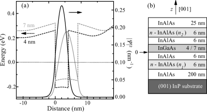
We experimentally investigate the PSH state in strain-free (001)-grown quantum well (QW) structures hosting a two-dimensional electron gas (2DEG). The QWs were designed to achieve almost equal linear Rashba and Dresselhaus coefficients, and , at zero gate voltage. Since is usually much smaller than in InGaAs 2DEGs Faniel11 , we needed to enhance and to reduce the built-in Rashba SOI. Since in QW structures , we designed sufficiently narrow QWs of width nm and 7 nm. Furthermore, was designed to be small at zero gate bias by preparing symmetric InGaAs QWs by placing two Si doping layers with densities and into the InAlAs barriers, each placed 6 nm away from the QW [see Fig. 1(b)]. Here, the higher doping level on the top side of the QW compensates the surface charges. Figure 1(a) shows the resulting conduction band structure and the electron distribution of the 4 nm and 7 nm QW structures. For the gate control of the PSH state, the epitaxial wafers were processed into m m Hall bar structures with an gate insulator and a Cr/Au top gate.

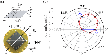
The photocurrent experiments were carried out with terahertz radiation of a pulsed laser JETP1982 with peak power of 5 to 10 kW, controlled by a reference photon drag detector JTPL1985 . Our laser generates single 100 ns pulses with a repetition rate of 1 Hz and wavelengths 90.5, 148 or 280 m. The corresponding photon energies are 13.7, 8.4 and 4.4 meV, respectively, much smaller than energy gap and subband separation. Therefore, the absorption is due to indirect transitions only within the lowest conduction subband. The configuration used for the spin-galvanic effect experiments is sketched in Fig. 2(a). For these measurements the samples were irradiated by circularly polarized light along the growth direction (-axis), and an external magnetic field with strengths up to 1 T was applied along the [100]-axis. The light generates a nonequilibrium spin polarization which, by means of the in-plane magnetic field, can be rotated into the QW plane. A spin-galvanic current , flowing due to asymmetric spin relaxation Ganichev2 , was measured [see Fig. 2(a)] via the voltage drop across a 50 load resistor. For these experiments, carried out at temperatures K and 296 K, the ungated samples, made of the same batches as the Hall bar structures, were used.
Figure 2(b) shows the signal of the spin-galvanic effect measured at room-temperature for the 4 nm QW along different in-plane directions, determined by the angle with respect to the fixed in-plane magnetic field . The current component, , parallel to the magnetic field is driven by the Rasba spin splitting, while the perpendicular component, is caused by the Dresselhaus SOI Ganichev2 ; Ganichev3 . The data presented in Fig. 2(b) can be well fitted by , with . This ratio is related to that between the linear Rashba and Dresselhaus SOI strengths, . The renormalized coefficient is described by Eq. (4) below.

The room-temperature results indicate that our ungated 4 nm QW samples are in a regime where the formation of a PSH is expected. At 5 K we find for the same sample showing a weak temperature dependence of this ratio. For the 7 nm QW with smaller we find similarly and at 296 and 5 K, respectively. Alternatively, the ratio between SOI strengths can also be extracted analyzing photocurrents arising from the circular photogalvanic effects Ganichev3 . We obtain a ratio for the ungated 4 nm sample at room temperature, in line with our SGE analysis.
The renormalized coefficient arises when decomposing in Eq. (2) [with ] into Iordanskii94
| (3) |
with
| (4) | |||||
| (5) |
Here and denote unit vectors. The measured photocurrents are related to the first-order harmonics ( and ) in the Fourier expansion of the nonequilibrium electron distribution function only Ganichev2 ; Ganichev3 . Consequently, the photocurrent is proportional to the linear Rashba term , see Eq. (1), and renormalized Dresselhaus term , see Eq. (4), but it is insensitive to the third harmonic of the cubic SOI term given by Eq. (5).
In a second, complementary, transport experiment we measured the quantum correction to the magneto-conductivity in the gated Hall bar structures in the presence of an external magnetic field , pointing perpendicularly to the QW plane Sch08 . At 1.4 K, various magneto-conductivity profiles were recorded for different strengths of the Rashba SOI by varying the gate voltage .
The carrier density , the mobility and the mean free path were extracted from sheet resistivity and periodicity of the Shubnikov-de Haas oscillations giving for the 4 nm (7 nm) sample () cm-2, (27000) cm2/Vs and (0.83) m at V and K.
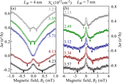
Figures 3(a) and (b) show the measured magneto-conductance profiles at different gate voltages for the 4 nm and 7 nm wide QWs, respectively. On the one hand, for the 7 nm QW, only WAL characteristics are observed, which get enhanced with increasing . On the other hand, most notably, the magneto-conductance for the 4 nm QW near changes from WAL to WL characteristics and back again to WAL upon increasing from 3.23 to 4.23 cm-2. The occurrence of WL (at cm-2) reflects suppressed spin relaxation, and the observed sequence WAL-WL-WAL unambiguously indicates that – even in presence of strong -cubic SOI – a PSH condition is fulfilled in the WL region.
Since the band profiles of the 4 nm and 7 nm wide quantum wells are very similar (see Fig. 1) we expect comparable values of the Rashba SOI. The difference in the bias dependence of the magneto-conductance of the two devices we hence ascribe to the different Dresselhaus SOI strengths . While for the 7 nm sample at zero bias the difference between and a small is too large to get tuned to comparable values, the larger of the 4 nm QW enables gate voltage tuning of to meet the condition for PSH formation, , associated with the occurrence of the WL peak.


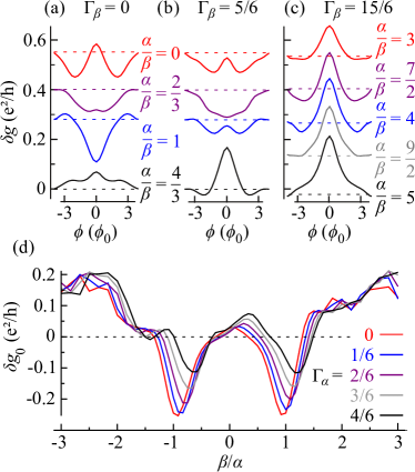
While the photocurrent experiments are insensitive to the third harmonic of the cubic term, Eq. (5), and thus reveal the ratio , the transport experiment probes spin randomization due to the entire SOI contribution, Eqs. (1) and (2). Hence the key question remains, namely: What is the general condition for the appearance of a PSH state, respectively WL, replacing the one, , for the linear case? To answer this question, and for an in-depth analysis of the transport experiments, we systematically studied the numerically computed crossover from WAL to WL in the magneto-conductance of disordered conductors under variation of the quantities treated as independent parameters in our model (thus neglecting the connection of and in realistic systems with fixed ). Our tight-binding calculations are based on an efficient recursive Green function algorithm Wimmer08 within the Landauer formalism. We consider a diffusive, two-dimensional phase-coherent mesoscopic conductor with periodic boundary conditions perpendicular to the transport direction. We employ the full SOI Hamiltonian, Eqs. (1) and (2), plus the contribution from an external perpendicular -field. While we cannot model the parameters of the 2D bulk experiment, since we are numerically limited to energy scales smaller than the realistic Fermi energies, we chose system sizes as well as energies and SOI strengths such that the ratio of the relevant parameters are comparable to experiment. These parameters consist of the ratios and which quantify the relative strength in the Hamiltonian (1,2) of cubic and linear SOI at a given Fermi momentum . By averaging over typically 100 disorder realizations we then computed the quantum (WL and WAL) correction by subtracting the average conductance at magnetic fields where coherent backscattering is suppressed from the average magneto-conductance , with being the magnetic flux through the system generated by the field .
Our main numerical results are summarized in Fig. 4. Panels (a,b) show magneto-conductance profiles for various ratios of for (a) vanishing and (b) finite . For the linear case, panel (a), we find, as expected, a WAL-WL-WAL crossover with pronounced WL dip for reflecting the PSH. For finite cubic SOI strength, , our numerics support the experimental findings [see Fig. 3(a)] that the crossover prevails, although with less pronounced WL dip. A rough estimate for the experiments with nm leads to , which is close to the numerical . Figure 4(c) is the numerical counterpart of Fig. 3(b), and predicts the absence of weak localization in a regime of increased and , where the factor by which is increased matches the value when the experiment at 4 nm [Fig. 3(a)] is compared to 7 nm [Fig. 3(b)]. Moreover, the strongest WL signal appears no longer at . In order to explore a refined condition for PSH behavior, we present in Fig. 4(d) as a function of for fixed and stepwise increasing values of from to . All curves display regimes of both WL and WAL behavior. We find two trends for increasing cubic SOI: (i) The WL dips diminish indicating the onset of spin relaxation, i.e., breaking of the exact PSH symmetry of the linear case. (ii) The conductance minima (WL) arising at for are linearly shifted towards larger values of with growing . We find a shift that differs from the shift entering into in Eq. (4). Hence our numerical analysis indicates that the condition for PSH formation deviates from common assumption . While often neglected, the cubic Dresselhaus terms (5) not only speed up spin relaxation but furthermore move the PSH point in three-dimensional SOI parameter space. This can also explain the small difference in the carrier density for observed WL-like behavior in transport () and for for the photocurrents () and suggests a refined condition for PSH-type behavior in the presence of -cubic terms.
In conclusion, we have demonstrated the existence and gate control of a PSH state in an InGaAs/InAlAs QW structure with strong, -cubic SOI by precise engineering the Rashba and Dresselhaus SOIs. The corresponding spin splittings have been deduced by utilizing methods based on the study of the anisotropies in WAL, SGE and CPGE analysis. By applying a gate electric field, a clearcut WAL-WL-WAL transition was observed. The results obtained by the different independent experimental techniques are in a good agreement, also with quantum transport calculations, and both experiments and theory reveal the robustness of the PSH. We thereby demonstrate that this state can be achieved even in structures with strong SOI and a substantial -cubic SOI contribution. The essential prerequisite is that for zero bias voltage and are close to each other, a condition which can be reached in very narrow and almost symmetric QWs due to a specially designed doping profile. However, in contrast to systems with dominating -linear spin splitting, the PSH is obtained for close, but nonequal Rashba and Dresselhaus strengths.
We thank M.M. Glazov for fruitful discussions. This work was partly supported by Grants-in-Aids from JSPS, MEXT, Japanese-German joint DFG research unit FOR 1483, Elitenetzwerk Bayern. LG thanks RFBR, Russian President grant for young scientists, and EU program “POLAPHEN” for support.
References
- (1) J. Nitta, T. Akazaki, H. Takayanagi, and T. Enoki, Phys. Rev. Lett. 78, 1335 (1997).
- (2) G. Engels, J. Lange, Th. Schäpers, and H. Lüth, Phys. Rev. B 55, R1958 (1997).
- (3) E.I. Rashba, Sov. Phys. Solid State 2, 1109 (1960).
- (4) G. Dresselhaus, Phys. Rev. 100, 580 (1955).
- (5) Note that a further source of SOI due to interface inversion asymmetry Roessler_Kainz_2002 enters in the same form into the spin-orbit Hamiltonian as that of the -linear BIA, and thus may change the magnitude of only.
- (6) U. Rössler and J. Kainz, Solid St. Commun. 121, 313 (2002).
- (7) I. Zutic, J. Fabian, and S.D. Sarma, Rev. Mod. Phys. 76, 323 (2004).
- (8) N.S. Averkiev and L.E. Golub, Phys. Rev. B 60, 15582 (1999).
- (9) J. Schliemann, J.C. Egues, and D. Loss, Phys. Rev. Lett. 90, 146801 (2003).
- (10) B.A. Bernevig, J. Orenstein, and S.-C. Zhang, Phys. Rev. Lett. 97, 236601 (2006).
- (11) X. Cartoixá, D. Z.-Y. Ting, and Y.-C. Chang, Appl. Phys. Lett. 83, 1462 (2003).
- (12) Y. Kunihashi, M. Kohda, H. Sanada, H. Gotoh, T. Sogawa, and J. Nitta, Appl. Phys. Lett. 100, 113502 (2012).
- (13) J. D. Koralek, C. P. Weber, J. Orenstein, B. A. Bernevig, S.-C. Zhang, S. Mack, and D. D. Awschalom, Nature 458, 610 (2009).
- (14) M. M. Glazov and L. E. Golub, Semicond. 40, 1209 (2006).
- (15) T.D. Stanescu and V. Galitski, Phys. Rev. B 75, 125307 (2007).
- (16) M. Duckheim, D. Loss, M. Scheid, K. Richter, I. Adagideli, and P. Jacquod, Phys. Rev. B 81, 085303 (2010).
- (17) M.C. Lüffe, J. Kailasvuori, and T.S. Nunner, Phys. Rev. B 84, 075326 (2011).
- (18) W. Knap, C. Skierbiszewski, A. Zduniak, E. Litwin-Staszewska, D. Bertho, F. Kobbi, J. L. Robert, G. E. Pikus, F. G. Pikus, S. V. Iordanskii, V. Mosser, K. Zekentes, and Yu. B. Lyanda-Geller, Phys. Rev. B 53, 3912 (1996).
- (19) F.G. Pikus and G.E. Pikus, Phys. Rev. B 51, 16928 (1995).
- (20) O. Zaitsev, D. Frustaglia, and K. Richter, Phys. Rev. B 72, 155325 (2005).
- (21) P. Wenk and S. Kettemann, Phys. Rev. B 83, 115301 (2011).
- (22) Earlier experiments Koga02 with gate-tunable strength showed only a transition from WL to WAL indicating merely the onset of SOI induced spin relaxation with increasing .
- (23) T. Koga, J. Nitta, T. Akazaki, and H. Takayanagi, Phys. Rev. Lett. 89, 046801 (2002).
- (24) S. D. Ganichev, V.V. Bel’kov, L. E. Golub, E. L. Ivchenko, Petra Schneider, S. Giglberger, J. Eroms, J. De Boeck, G. Borghs, W. Wegscheider, D. Weiss, and W. Prettl, Phys. Rev. Lett. 92, 256601 (2004).
- (25) V.V. Bel’kov and S.D. Ganichev, Semicond. Sci. Technol. 23, 114003 (2008).
- (26) S. Giglberger, L. E. Golub, V. V. Bel’kov, S. N. Danilov, D. Schuh, Ch. Gerl, F. Rohlfing, J. Stahl, W. Wegscheider, D. Weiss, W. Prettl, and S. D. Ganichev, Phys. Rev. B 75, 035327 (2007).
- (27) S. Faniel, T. Matsuura, S. Mineshige, Y. Sekine, and T. Koga, Phys. Rev. B 83, 115309 (2011).
- (28) S. D. Ganichev, S. A. Emel’yanov, and I. D. Yaroshetskii, JETP Lett. 35, 368 (1982).
- (29) S. D. Ganichev, Ya. V. Terent’ev, and I. D. Yaroshetskii, Sov. Tech. Phys. Lett. 11, 20 (1985).
- (30) S. V. Iordanskii, Yu. B. Lyanda-Geller, and G. E. Pikus, JETP Lett. 60, 206 (1994).
- (31) M. Scheid, M. Kohda, Y. Kunihashi, K. Richter, and J. Nitta, Phys. Rev. Lett. 101, 266401 (2008).
- (32) M. Wimmer and K. Richter, J. Comput. Phys. 228, 8548 (2009).