Plasmons in electrostatically doped graphene
Abstract
Graphene has raised high expectations as a low-loss plasmonic material in which the plasmon properties can be controlled via electrostatic doping. Here, we analyze realistic configurations, which produce inhomogeneous doping, in contrast to what has been so far assumed in the study of plasmons in nanostructured graphene. Specifically, we investigate backgated ribbons, co-planar ribbon pairs placed at opposite potentials, and individual ribbons subject to a uniform electric field. Plasmons in backgated ribbons and ribbon pairs are similar to those of uniformly doped ribbons, provided the Fermi energy is appropriately scaled to compensate for finite-size effects such as the divergence of the carrier density at the edges. In contrast, the plasmons of a ribbon exposed to a uniform field exhibit distinct dispersion and spatial profiles that considerably differ from uniformly doped ribbons. Our results provide a road map to understand graphene plasmons under realistic electrostatic doping conditions.
PlasmonsRaether (1988) –the collective oscillations of conduction electrons in metals– are capable of confining electromagnetic energy down to deep sub-wavelength regions. They can also enhance the intensity of an incident light wave by several orders of magnitude. These phenomena are the main reason why the field of plasmonics is finding a wide range of applications that include single-molecule sensing,Rodríguez-Lorenzo et al. (2009) nonlinear optics,Danckwerts and Novotny (2007) and optical trapping of nanometer-sized objects.Juan et al. (2011)
Recently, confined plasmons have been observed and spatially mapped in doped graphene.gra The level of doping in this material can be adjusted by exposing it to the electric fields produced by neighboring gates. Electrostatic doping has actually been used to demonstrate plasmon-frequency tunabilitygra and induced optical modulations in the THzJu et al. (2011) and infraredFei et al. (2011) response of graphene.
The two-dimensional (2D) band structure of pristine graphene consists of two cones filled with valence electrons and two empty inverted cones joining the former at the so-called Dirac points, which mark the Fermi level. Extra electrons or holes added to this structure form a 2D electron or hole gas that can sustain surface plasmons.Shung (1986); Wunsch et al. (2006) Compared to noble-metal plasmons, graphene modes are believed to be long-lived excitations.Jablan et al. (2009) But most importantly, their frequency can be controlled via the above-mentioned electrostatic doping.Ju et al. (2011); Fei et al. (2011); gra For example, in homogeneous suspended graphene, a perpendicular DC electric field applied to one side of the carbon sheet is completely screened by an induced surface charge density , and this in turn situates the Fermi level at an energy relative to the Dirac points.Castro Neto et al. (2009) Here, m/s is the Fermi velocity of graphene.
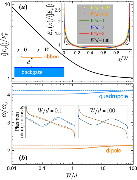
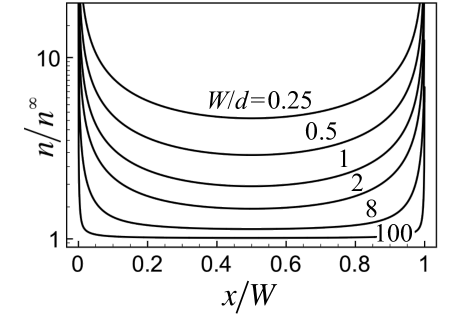
Plasmons in doped graphene nanostructures have been generally studied by assuming a uniform doping electron density .Vakil and Engheta (2011); Koppens et al. (2011) But in practice is inhomogeneous and depends on the actual geometrical configuration. For example, in a ribbon of width placed at a distance from a planar biased backgate, shows a dramatic pileup near the edges, as it is well known in microstrip technology,Wheeler (1964, 1977); Silvestrov and Efetov (2008); Vasko and Zozoulenko (2010) leading to divergent local levels, as shown in the inset of Fig. 1(a) for various values of . More precisely, diverges as with the distance to the edge (and hence, ). The average of the Fermi energy over the ribbon area [, see Fig. 1(a)] is very different from the limit () and diverges asana in the narrow ribbon limit () for constant bias potential . Therefore, the question arises, how different are the plasmon energies and field distributions in actual doped graphene nanostructures compared to those obtained for uniformly doped graphene?
Here, we analyze plasmons in doped graphene ribbons under different geometrical configurations. Specifically, we study backgated single ribbons, co-planar parallel ribbon pairs of opposite polarity, and single ribbons immersed in a uniform external electric field. For simplicity, we describe the frequency-dependent conductivity of doped graphene in the Drude model as , where is a small relaxation rate. The doping electron density is obtained from electrostatic boundary-element calculations, while the plasmon frequencies are computed using a discrete surface-dipole approximation (DSDA), as explained in Appendix C.
Backgated ribbons.- A first conclusion extracted from Fig. 1(a) is that the level of doping, quantified in the Fermi energy, is not well described by the simple capacitor analysis of the geometry. Normalizing to the average value , we find Fermi-energy profiles that vary between a well of sharp corners for large and a smoother, converged shape for small [upper inset of Fig. 1(a)]. The former limit corresponds to the ribbon in close proximity to the backgate, in which is nearly uniform. In contrast, at large separations () we find a profile determined by the interaction with a distant image, which converges to a well-defined shape up to an overall factor evolving as shown in the main plot of Fig. 1(a).
It is convenient to normalize the ribbon plasmon frequencies to , so that is a dimensionless number, independent of the specific ribbon width and gate voltage (i.e., ), as proved in Appendix B. For example, with nm and eV, we find eV and a dipole plasmon energy eV (wavelength m). With this normalization, shows just a mild dependence on for the dipolar and quadrupolar modes [Fig. 1(b)]. The corresponding induced densities (insets) are only slightly affected by the change in doping profile relative to uniform doping (i.e., the average level of doping is a dominant parameter, and the effect of edge divergences is only marginal). In conclusion, the plasmon frequencies and induced densities can be approximately described by assuming a uniform Fermi energy in backgated ribbons, thus supporting the validity of previous analyses for this configuration,Koppens et al. (2011); Nikitin et al. (2011); Christensen et al. (2012) although the Fermi energy has to be appropriately scaled as shown in Fig. 1(a) to compensate for the effect of finite ratios.
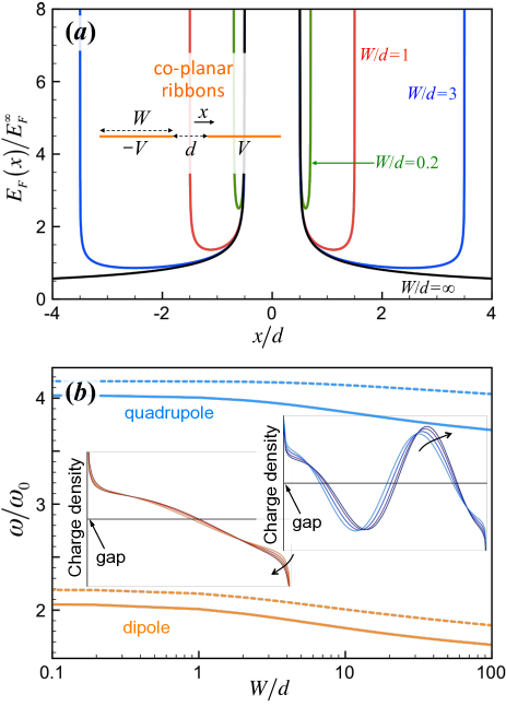
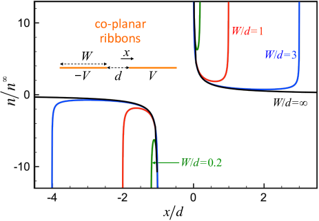
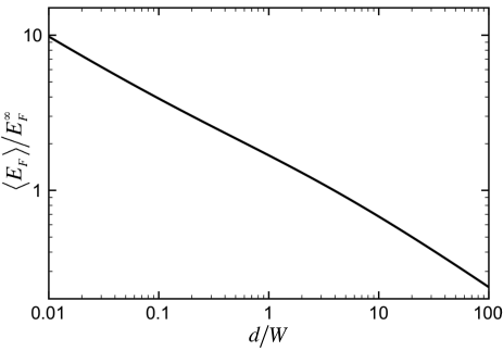
Two co-planar parallel graphene ribbons.- Two neighboring ribbons can act both as plasmonic structures and as gates. We explore this possibility in Fig. 2, where the ribbons are taken to be oppositely polarized. This produces doping profiles as shown in Fig. 2(a), which evolve from a shape similar to the one obtained for the single ribbon of Fig. 1 in the small-ribbon limit at large ribbon-pair separations, towards a converged profile near the gap in the limit. Again, plasmons in this structure are very similar to those of neighboring uniformly doped ribbons [see Fig. 2(b)], provided one compares for the same value of the average Fermi energy . The separation dependence of is shown in Appendix A. Incidentally, plasmons in pairs of uniform ribbons have been thoroughly described and the evolution of the plasmon frequency with distance explained in a recent publication,Christensen et al. (2012) including the redshift with decreasing .
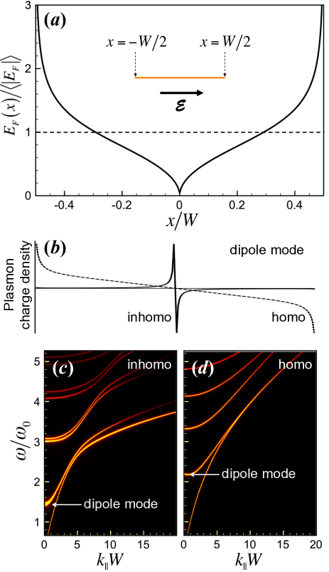
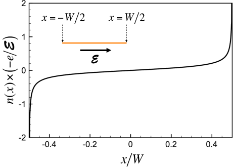
Doping through a uniform electric field.- A disadvantage of the above doping schemes is the fabrication process involved in adding contacts that allow electrically charging the graphene, which can be a source of defects in the carbon layer. This could be avoided by doping through an external electric field produced by either distant gates or low-frequency radiation. The graphene would then remain globally neutral. This possibility is analyzed in Fig. 3, where we consider a ribbon subject to a uniform electric field directed across its width. The doping profile [Fig. 3(a)] is again exhibiting a divergence of at the edges, and it vanishes at the center of the ribbon, where the doping density changes sign (see Appendix A.3). Following the methods described in Appendix A.3, we find the relation . The resulting dipolar plasmon [Fig. 3(b), solid curve] displays a large concentration of induced charges near the center of the ribbon, in contrast to the dipole plasmon obtained for a homogeneous doping density (dashed curve). This inhomogeneous dipole-charge concentration is induced by the vanishing of the doping charge density, which can be understood as a thinning of the effective graphene-layer thickness, similar to what happens near the junction of two barely touching metallic structures (e.g., two spheresRomero et al. (2006)).
We have so far discussed plasmons that are invariant along the length of the ribbon (i.e., as those excited by illuminating with light incident perpendicularly to the graphene). But now, we show in Fig. 3(c),(d) the full plasmon dispersion relation as a function of frequency and wave vector parallel to the ribbon, both for inhomogeneous doping produced by an external uniform field [Fig. 3(c)] and for a ribbon with uniform doping density [Fig. 3(d)]. The dispersion relations are rather different in both situations, with the inhomogeneous ribbon showing a denser set of modes, as well as more localization in the lowest-energy plasmons for large , as we show in Appendix C by means of near-field plots for the lowest-energy modes of both types of ribbons.
Finally, let us mention that the inelastic plasmon decay rate is given by within the Drude model in uniformly doped structures.Christensen et al. (2012) However, depends on position for inhomogeneous doping. Using the DC mobility , one can estimate s-1 for eV and a typical measured mobility cmVs.Novoselov et al. (2004); Zhang et al. (2005) Noticing that the local contribution to inelastic losses is proportional to (i.e., independent of ), we conclude that the inhomogeneity of is however translated into a uniform spatial distribution of losses.
Conclusions.- We have shown that the plasmons of doped graphene ribbons are highly sensitive to the inhomogeneities of the doping charge density produced by realistic electrostatic landscapes. The doping profile can be engineered by adjusting the configuration of the gates relative to the graphene. We find an interesting scenario when a uniform external electric field is used to dope the graphene, leading to plasmons with very different characteristics (e.g., induced charges piling up near the center of the ribbon) compared to those of uniformly doped graphene (in which plasmons pile up at the edges). This configuration can be used to avert losses associated with nonlocal effects at the edges, which are expected to be significant.Thongrattanasiri et al. (2012) The present study can be straightforwardly extended to other configurations, such as finite graphene nanoislands exposed to either backgates or side gates. Electrostatic charge accumulation at sharp edges can offer an additional handle to manipulate plasmon modes. In addition to the possibilities explored in this paper, one can use biased tips to produce localized disk-like doping areas at designated positions targeted by simply moving the tips above a graphene flake. In conclusion, the design of electrostatic landscapes becomes a useful tool to engineer graphene plasmons.
We would like to thank Enrique Bronchalo for helpful discussions. This work has been supported by the Spanish MICINN (MAT2010-14885 and Consolider NanoLight.es) and the European Commission (FP7-ICT-2009-4-248909-LIMA and FP7-ICT-2009-4-248855-N4E).
Appendix A Electrostatic calculation of doping surface charge distributions
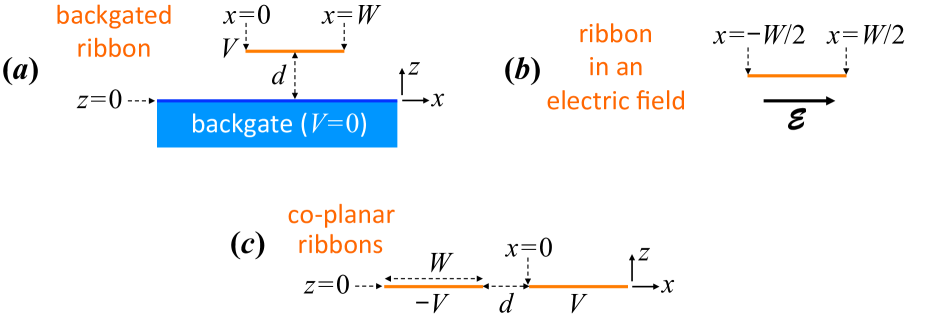
We consider three different geometries for electrically doping graphene, as illustrated in Fig. 4. Geometries in Figs. 4(a),(c) refer to doping of biased graphene ribbons, which accumulate a net electric charge. In contrast, the ribbon of Fig. 4(b), exposed to an external uniform field, has zero total charge. The charge distribution in a backgated ribbon [Fig. 4(a)] has been reported in the past,Wheeler (1964, 1977); Silvestrov and Efetov (2008); Vasko and Zozoulenko (2010) particularly in the context of microstrip technology,Wheeler (1964, 1977) but we provide here a general procedure to calculate it based upon boundary elements, which we extend to other geometries under consideration.
A.1 Backgated graphene ribbon
A ribbon placed at a potential relative to a backgate [Fig. 4(a)] displays a charge density that can be calculated using the method of images (notice that is the doping electron density). The charge depends on the coordinate across the ribbon , which varies in the range , where is the width. Using the method of images, this problem is equivalent to two parallel ribbons vertically separated by a distance and placed at potentials (upper ribbon) and (lower ribbon), so that the backgate plane () is at zero potential. The lower ribbon is thus represented by a charge density . The potential at in the upper ribbon is then given by
| (1) |
Analytically performing the integral along the coordinate (perpendicular to the plane of Fig. 4) and using the notation , , and
Eq. (1) reduces to
| (2) |
where
We solve this integral equation by discretizing through a set of equally spaced points , with . Equation (2) is then approximated as
| (3) |
where
| (4) |
is an integral over the interval surrounding point . We have assumed that is a smooth function, and although we find later that it diverges as near the edges (see main paper), this divergence is integrable and contributes negligibly to the total integral for . From here, the charge distribution is found by inverting the matrix , so that
| (5) |
In practice, this method converges for . Similar convergence is obtained for the geometries considered in Secs. A.2 and A.3. Each curve in Fig. 1(a) of the main paper is actually consisting of two curves obtained with and , and one cannot tell the difference between them on the scale of the plot. Finally, notice that the uniform electron density in the limit is given by . Also, we obtain the average of the Fermi energy normalized to the limit as
where m/s is the Fermi velocity. (Incidentally, we consider the absolute value of because the graphene response is nearly insensitive to the sign of .)
Figure 5 shows examples of doping charge densities from which we have extracted the Fermi energies shown in the inset of Fig. 1(a) of the main paper.
A.2 Two co-planar parallel ribbons set at opposite potentials
We can repeat the same analysis as in Sec. A.1 for two ribbons arranged as shown in Fig. 4(c) and set at potentials (left ribbon) and (right ribbon). The separation between ribbons is , and is chosen at the left edge of the right ribbon. Equations (2)-(5) remain valid when we consider the charge distribution in the right ribbon, but now the kernel of Eq. (2) becomes
The charge density in the left ribbon is found from the symmetry .
Figure 6 shows examples of doping charge densities from which we have extracted the Fermi energies shown in Fig. 2(a) of the main paper. The average Fermi energy is shown in Fig. 7 as a function of .
A.3 Graphene ribbon in a uniform electric field
For a ribbon subject to an external uniform electric field, only the component parallel to the ribbon can produce charge redistributions and local doping [see Fig. 4(b)]. Following the same procedure as in Sec. A.1, and taking the ribbon to be placed at zero potential, we can write
where the first term is the scalar potential produced by the external field. Now, using the normalization , the above equation reduces to
where
We use the discretization to write an expression similar to Eq. (3), where is still given by Eq. (4) with . Finally, the electron density is obtained from
The doping charge density obtained from this equation is represented in Fig. 8. From here, we find a local Fermi energy as shown in Fig. 3(a) of the main paper. The average Fermi energy is found to be .
Appendix B Scaling of plasmon frequencies in the Drude model
The electric scalar potential associated with the plasmon modes in a doped graphene planar nanostructure satisfies the self-consistent electrostatic equation
| (6) |
where an time dependence is undertood and all quantities are evaluated at the graphene plane (i.e., coordinates and are in that plane). This equation represents the field induced by the self-consistent surface-charge density, which is calculated from the continuity equation as in terms of the current , and this is in turn proportional to the in-plane electric field via , where is the conductivity. Incidentally, outside the graphene, so that presents a jump at the graphene edge, the gradient of which generates an edge charge density. Equation (6) is valid for small patterning lengths compared to the light wavelength. The constant takes the values for suspended graphene in vacuum, for graphene embedded in a uniform dielectric of permittivity , or for graphene supported on a substrate.Christensen et al. (2012) Now, we consider the Drude model for the conductivity,
| (7) |
where and the dependence comes from the inhomogeneous electron density (see Sec. A), which locally situates the Dirac points at an energy relative to the Fermi level.Castro Neto et al. (2009)
From the analysis of Sec. A, we can write the Fermi energy distribution as , where is a dimensionless envelope function. Likewise, distances can be scaled with a characteristic length as . Then, Eq. (6) becomes
where
is a dimensionless eigenvalue. The modes of the system satisfy this equation for specific choices of , and therefore, we conclude that the plasmon energies can be naturally normalized to the frequency
| (8) |
Obviously, does not depend on the specific choice of (the doping level), (the size of the system), or (the dielectric environment), and consequently, we present results normalized in this way in the main paper, which are universal for the kind of geometries under consideration, provided we stay within the limits of validity of the Drude model (i.e., , and smaller than the optical phonon energy eVJablan et al. (2009)). Additionally, because the electrostatic eigensystem is Hermitian,Ouyang and Isaacson (1989) the eigenvalues are real, and therefore, the plasmon frequencies have imaginary part , so that the plasmon lifetime is , independent of geometrical and physical parameters within the Drude approximation.
Appendix C Computation of plasmon frequencies and near fields
We solve the electrostatic problem of Eq. (6) by describing the graphene as a periodic array of surface dipoles with a small period compared to the characteristic lengths of the structure. This is the discrete surface-dipole approximationDSD (DSDA), in which the polarizability of each element is taken such that a layer formed by a uniform lattice of dipoles has the same conductivity as a uniform layer of graphene. The sum over dipole elements along is performed before a self-consistent solution is sought, and therefore, the numerical problem reduces to solving a set of linear equations with variables (the dipole components along both and directions), where is the number of dipoles across . In practice, convergence is achieved with a few hundred dipoles for the dimensions considered in this work. Here, we have modified this method by allowing each element to depend through on the spatial position along .
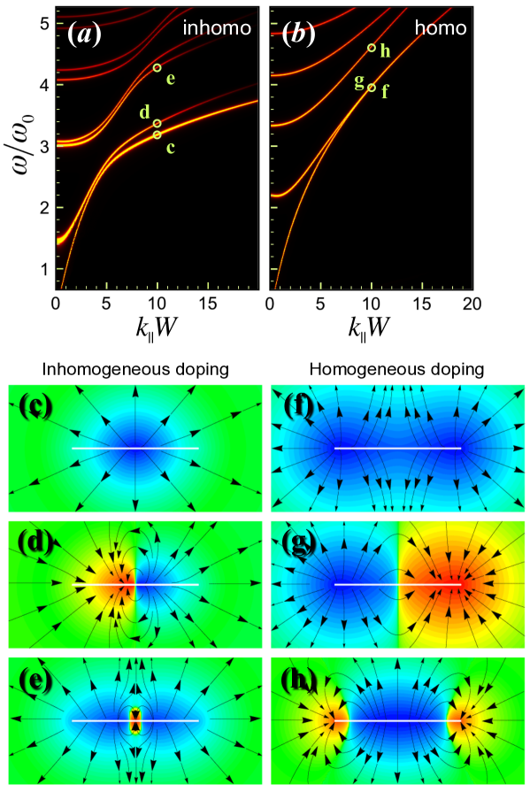
As an example of calculation, we show in Fig. 9(a),(b) plasmon dispersion diagrams for both an inhomogeneously doped ribbon under the same conditions as in Fig. 8 and a homogeneously doped ribbon. These plots are the same as Fig. 3(c),(d) of the main paper. We also show the near fields calculated for the three lowest-energy modes in each case, with . These are plasmons of monopole (c,f), dipole (d,g), and quadrupole (e,h) character. In the inhomogeneous ribbon, the modes are associated with large field enhancement near the center. In contrast, the uniform ribbon hosts modes with large field enhancement near the edges.
References
- Raether (1988) H. Raether, Surface Plasmons on Smooth and Rough Surfaces and on Gratings, vol. 111 of Springer Tracks in Modern Physics (Springer-Verlag, Berlin, 1988).
- Rodríguez-Lorenzo et al. (2009) L. Rodríguez-Lorenzo, R. A. Álvarez-Puebla, I. Pastoriza-Santos, S. Mazzucco, O. Stéphan, M. Kociak, L. M. Liz-Marzán, and F. J. García de Abajo, J. Am. Chem. Soc. 131, 4616 (2009).
- Danckwerts and Novotny (2007) M. Danckwerts and L. Novotny, Phys. Rev. Lett. 98, 026104 (2007).
- Juan et al. (2011) M. L. Juan, M. Righini, and R. Quidant, Nat. Photon. 5, 349 (2011).
- (5) J. Chen et al., arXiv:1202.4996v1; Z. Fei et al., arXiv:1202.4993v1.
- Ju et al. (2011) L. Ju, B. Geng, J. Horng, C. Girit, M. Martin, Z. Hao, H. A. Bechtel, X. Liang, A. Zettl, Y. R. Shen, et al., Nat. Nanotech 6, 630 (2011).
- Fei et al. (2011) Z. Fei, G. O. Andreev, W. Bao, L. M. Zhang, A. S. McLeod, C. Wang, M. K. Stewart, Z. Zhao, G. Dominguez, M. Thiemens, et al., Nano Lett. 11, 4701 (2011).
- Shung (1986) K. W. K. Shung, Phys. Rev. B 34, 979 (1986).
- Wunsch et al. (2006) B. Wunsch, T. Stauber, F. Sols, and F. Guinea, New J. Phys. 8, 318 (2006).
- Jablan et al. (2009) M. Jablan, H. Buljan, and M. Soljac̆ić, Phys. Rev. B 80, 245435 (2009).
- Castro Neto et al. (2009) A. H. Castro Neto, F. Guinea, N. M. R. Peres, K. S. Novoselov, and A. K. Geim, Rev. Mod. Phys. 81, 109 (2009).
- Vakil and Engheta (2011) A. Vakil and N. Engheta, Science 332, 1291 (2011).
- Koppens et al. (2011) F. H. L. Koppens, D. E. Chang, and F. J. García de Abajo, Nano Lett. 11, 3370 (2011).
- Wheeler (1964) H. A. Wheeler, IEEE Trans. Microwave Theory Tech. 12, 280 (1964).
- Wheeler (1977) H. A. Wheeler, IEEE Trans. Microwave Theory Tech. 25, 631 (1977).
- Silvestrov and Efetov (2008) P. G. Silvestrov and K. B. Efetov, Phys. Rev. B 77, 155436 (2008).
- Vasko and Zozoulenko (2010) F. T. Vasko and I. V. Zozoulenko, Appl. Phys. Lett. 97, 092115 (2010).
- (18) This asymptotic expression can be easily derived by considering a thin biased wire placed above a backgate, and it might be useful to achieve large doping levels without electrical breakdown.
- Nikitin et al. (2011) A. Y. Nikitin, F. Guinea, F. J. García-Vidal, and L. Martín-Moreno, Phys. Rev. B 84, 161407(R) (2011).
- Christensen et al. (2012) J. Christensen, A. Manjavacas, S. Thongrattanasiri, F. H. L. Koppens, and F. J. García de Abajo, ACS Nano 6, 431 (2012).
- Romero et al. (2006) I. Romero, J. Aizpurua, G. W. Bryant, and F. J. García de Abajo, Opt. Express 14, 9988 (2006).
- Novoselov et al. (2004) K. S. Novoselov, A. K. Geim, S. V. Morozov, D. Jiang, Y. Zhang, S. V. Dubonos, I. V. Grigorieva, and A. A. Firsov, Science 306, 666 (2004).
- Zhang et al. (2005) Y. Zhang, Y. W. Tan, H. L. Stormer, and P. Kim, Nature 438, 201 (2005).
- Thongrattanasiri et al. (2012) S. Thongrattanasiri, A. Manjavacas, and F. J. García de Abajo, ACS Nano 6, 1766 (2012).
- Ouyang and Isaacson (1989) F. Ouyang and M. Isaacson, Philos. Mag. B 60, 481 (1989).
- (26) F. J. García de Abajo and S. Thongrattanasiri, unpublished.