,
,
Sliding charge-density-wave in two-dimensional rare-earth tellurides
Abstract
Nonlinear transport properties are reported in the layered DyTe3 compound at temperature below the charge-density-wave (CDW) transition, K. Conductivity is increasing sharply above the threshold electric field. Under application of a rf field Shapiro steps are clearly observed. These features demonstrate for the first time CDW sliding in two-dimensional compounds.
pacs:
72.15.Nj, 71.45.Lr, 61.44.FwInteraction between pairs of quasiparticles often leads to broken-symmetry ground states in solids. Typical examples are the formation of Cooper pairs in superconductors, and charge (CDW) and spin (SDW) density waves driven by electron-phonon and electron-electron interactions respectively Gruner . Density wave formation is favoured by nesting of parallel Fermi surface (FS) at and . The first canonical example was found fifty years ago when the antiferromagnetism in Cr was identified as an incommensurate SDW transition Overhauser62 resulting from nesting of electron-hole pockets sheets having similar shape Lomer62 (for a review see also Fawcett88 ; Fawcett94 ).
A CDW ground state is characterized by a concomitant spatial modulation of the electron density and a periodic lattice distortion with the same wave vector inducing opening of a gap in the electron spectrum. The coupled electron-phonon which leads to the Kohn anomaly at high temperature is split into two different modes below the Peierls transition: on optical mode (called amplitudon) and on acoustic phase mode, or phason Gruner .
For ideal 1D conductors, the phase mode exists at zero frequency at realizing the Goldstone mode in systems with spontaneously broken continuous symmetry. Then, a persistent current is provided by the sliding motion of the CDW Frohlich54 . However various mechanisms such as impurities, interchain interaction or commensurability pin the phase of the CDW and introduce a gap in the excitation of the phase mode which prevents the dc Fröhlich conductivity but leads to a large low frequency ac conductivity. The pinning energy must be overcome to initiate the CDW sliding; that can be achieved by the application of an electric field of a sufficient strength Gruner . In addition to the increase of conductivity associated with collective CDW motion above a threshold electric field, , a periodic time dependent voltage is generated as well as a broad band noise Gruner . Sliding CDW properties have been observed in inorganic NbSe3, TaS3, K0.3MoO3, (TaSe4)2I as well as in organic (TTF-TCNQ), (TMTSF)2X, (Per)2M(Mnt)2 and (fluoranthene)2X one-dimensional compounds Monceau12 .
Attempts to detect sliding effect in 2D systems are, up to now, unsuccessful. Thus, absence of nonlinearity in current-voltage characteristics (IVc) was reported in 2H- TaSe2 and 1T-TaSe2 up to electric field 1 V/cm and 10 V/cm respectively DiSalvo80 . These values are much higher that typical in 1D compounds. One possible reason might be a commensurability pinning resulting from the triple- structure with three wave vectors of equal amplitude, apart.
Sliding properties were also searched in other 2D structures. Thus, 2D quantum systems of electrons of extremely low disorder in GaAs/AlGaAs heterejunctions were shown to exhibit conduction typical of pinned CDWs Goldman90 . Microwave resonance in conductivity were understood as the pinning mode of the electron or charge ordered crystal Chen03 ; Sambandamurthy08 . For reentrant integer quantum Hall states, a sharp threshold and a periodic voltage associated with broad band noise were measured Cooper03 . Although such effects are very similar to characteristic features of CDW sliding, the very low frequency of the ac voltage generated in the non-linear state disregards the analogy with a simple CDW model.
It was recently claimed that the superstructure in the stripe phase of a thin film of La0.5Ca0.5MnO3 was a prototype CDW with collective transport properties Cox08 . This statement was based on observation of hysteresis in IVc and broad band noise. However, no clear threshold field or ac voltage generation was observed, that was explained by a large impurity density. Broad band noise observation in manganites was also reported in Wahl03 ; Barone09 . Nonlinear transport properties in manganites were challenged in Fisher10 .
Recently a new class of layered compounds, namely rare-earth tritellurides Te3 ( =Y, La, Ce, Nd, Sm, Gd, Tb, Ho, Dy, Er, Tm), has raised an intense research activity on CDW DiMasi95 ; Brouet08 ; Ru08 . These systems exhibit an incommensurate CDW through the whole series with a wave vector with a Peierls transition temperature above 300 K for the light atoms (La, Ce, Nd). For the heavier (Dy, Ho, Er, Tm) a second CDW occurs with the wave vector . The superlattice peaks measured from X-ray diffraction are very sharp and indicate a long range 3D CDW order Ru08 .
All Te3 compounds have the same orthorhombic structure () in the unmodulated state. The structure is formed of blocks of Te layers sandwiched between the Te- layers and stacked together along the -axis with weak van der Waals gap (Å) between them. In the () plane Te–Te distances are 3.1 Å (to be compared to the covalent Te–Te bond of 2.8 Å). The charge transfer from ions to Te square yields the -band for Te square sheets to be partially filled. Band structure calculated with simple tight-binding approximation reveals that the electronic bands of derive from and in plane Te orbitals, leading to a simple FS. Splitting of the bands occurs due to bilayer Te sheets in the unit cell shifted one with respect to the other by . The hopping between orbitals along a given direction ( or ), , is much larger than the hopping between same orbitals on neigbour rows, . In addition hopping between second-neigbour, , mixes the and bands. Typically it was estimated eV, eV and eV Yao06 . The finite value of introduce the warping of FS; is much larger than 300 K, indicating that 1D approximations are not applicable to Te3 compounds.
Amplitude CDW excitations in Te3 were probed by Raman scattering Lavagnini08 ; Lavagnini10 and femtosecond pump-probe spectroscopy Yusupov10 . On the other hand, collective charge phase excitations could not be observed in far-infrared measurements Lavagnini09 due to screening by the residual metallic component at the Fermi surface. But the phase collective mode is accessible through nonlinear transport properties as we report hereafter in DyTe3. It is the first evidence of CDW sliding in a quasi-2D systems.
DyTe3 was chosen because in this compound the CDW appears just at room temperature at K and the lower CDW at K is the largest in the Te3 series. The component of the wavevector along was found to be 0.2984 Malliakas08 (or 0.7061 according to whether the 2D Brillouin zone for a single Te plane or the 3D Brillouin zone for the unit cell is considered). This value is slightly far away from 2/7 or 5/7 (0.286 or 0.714) estimated from band filling resulting from charge transfer between ions and Te sheets.
A slightly modified method described in Ru06 has been used for the growth of single crystal of DyTe3: single crystals were grown by a self-flux technique under purified argon atmosphere in a sealed quartz tube. High quality starting elements were used: 4N, Te 6N and the molar composition of the binary system was: (DyTe3 + 90 Te). The mixture has been heated, in a same run, at 550∘C and 850∘C respectively for 2 days before cooling down at with a ramping of hour to 450∘C and then quenched in air to room temperature. The millimeter scale plate-like single crystals were mechanically extracted from the bulk. The -axis has been checked to be perpendicular to the large surface of crystals and its value refined Å for DyTe3.
Thin single-crystal samples were prepared by micromechanical exfoliation of relatively thick crystals glued on a sapphire substrate. From homogeneous square single crystals with thickness m, we cut bridges with width m. Measurements of current-voltage characteristics (IVs) and their derivatives have been performed with a conventional 4-probe configuration. Contacts were prepared from In by cold soldering. The distance between potential probes varied in the range mm. For studying nonstationary effects a radiofrequency (rf) current was superposed on the dc current using current contacts connected with the generator via two capacitors.

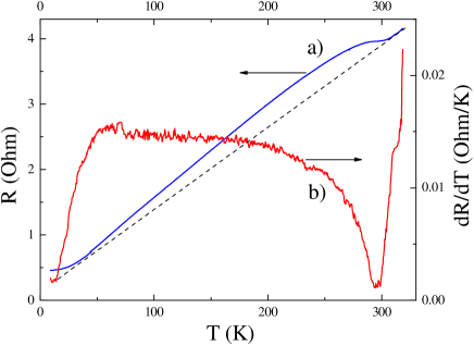
Fig.1 shows the characteristic (a) and (b) dependencies in the (a–c) plane for one of the DyTe3 sample we measured. The small increase in resistance below K is the signature of the Peierls transition in this compound. On the this effect is much more pronounced. Our data in Fig.1 are very similar to those in Ru08 . No visible variation of the resistance was detectable for the CDW transition at .
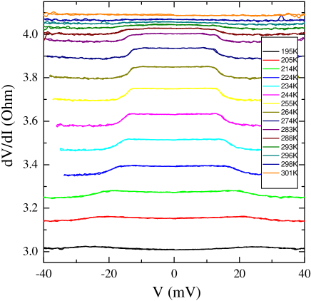
In Fig.2 we have drawn the differential IVc in the temperature range K for a sample with a thickness of 0.5 m. A pronounced non-linearity is observed below 300 K. Although the amplitude of this non-linearity is small (), the threshold behavior typical for the transition to the sliding CDW state is clearly seen: the IVs are Ohmic for voltage less than some threshold voltage , and for voltages in excess of this value the differential resistance, , decreases sharply. At temperatures K the IVs are Ohmic without any non-linearities except very little Joule heating which appears as a small parabolic increase of the differential resistance. For thicker samples, the threshold behavior is smeared by Joule heating.

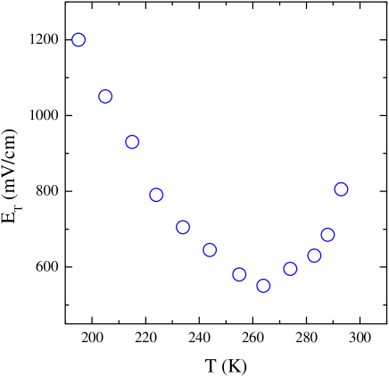
The very sharp onset of the observed non-linearity allows to determine the temperature dependence of the threshold electric field, , which is shown in Fig.3. As can be seen, initially decreases in the temperature range K and increases when the temperature is decreased further. Note that such a behavior is typical for in quasi-one dimensional systems with a CDW Gruner .

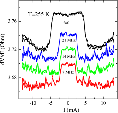
It is well known that the joint application of dc and rf driving fields leads to appearance of harmonic and subharmonic Shapiro steps in the dc IV characteristics of 1D CDWs Gruner . In the present work we have also observed Shapiro steps at such experimental conditions. Fig.4 shows dependencies at K under application of a rf field with a frequency of 7, 14 and 21 MHz with the same rf-power. For comparison, the static (without rf field) differential IV measured at this temperature is also shown. The curves are shifted relatively to each over for clarity. First of all, note that application of a rf electric field leads to reduction of the threshold electric field . At the same time, Shapiro steps appear in the characteristic as a sharp maxima in the differential resistance. With increasing frequency the distance between neighbouring maxima increases proportionally to the frequency.

The observation of Shapiro steps is one of the characteristic features of a CDW collective transport Gruner . Thus, the observed non-linearities of dc IVc together with the observation of Shapiro steps evidently indicate that a contribution to the electrical transport from the collective CDW motion takes place in the 2D CDW DyTe3 compound.
It is worth to note that the effect of CDW on the resistance in the (a–c) plane is very weak (see Fig.1) and consists only a few % of increase below . In fact the larger effect is along the -axis perpendicularly to the Te sheets Ru08 . It is commonly explained that the reduction of the Fermi surface (FS) by opening of the CDW gap reduces the scattering of electrons and therefore the conductivity. From angle-resolved photoemission (ARPES) and optical studies it was shown that at low temperature about 30% -40% of FS in ErTe3 and HoTe3 is affected by formation of the CDW Pfuner10 . The small decrease of conductivity below may indicate that electrical transport does not significantly involve bands on which the CDWs occur.
Although the temperature dependence of the gap amplitude was found to follow a BCS type, the ratio is much larger than the mean field 3.52 value. Such a large magnitude was already measured in transition metal dichalcogenides, and specifically in 2H-TaSe2. That led McMillan to develop a strong coupling model for systems with short coherence length where phonon frequencies are modified over large parts of reciprocal space McMillan77 . The strong electron coupling is also revealed by the stretching of the lattice along the -axis resulting from the CDW formation Ru08 .
In conclusion we have shown that the phase of the 3D long range order CDW in the layered DyTe3 compound can easily slide above a small threshold field. We demonstrate thus, for the first time, CDW sliding in two-dimensional compounds.
Acknowledgements.
The authors are thankful to J. Marcus for help in the sample preparation. The work has been supported by Russian State Fund for the Basic Research (No. 11-02-01379), and partially performed in the frame of the CNRS-RAS Associated International Laboratory between Institute Neel and IRE ”Physical properties of coherent electronic states in coherent matter”.References
- (1) G. Grüner, Density Waves in Solids (Addison – Wesley, Reading, Massachusetts, 1994), L. Gor’kov and G. Grüner Charge Density Waves in Solids (Amsterdam: Elsevier Science, 1989), Electronic Crystals 08 edited by S. Brazovskii, P. Monceau and N. Kirova, (Physica B, vol 404, Issues 3-4, 2009).
- (2) A.W. Overhauser, Phys. Rev. 128, 1437 (1962).
- (3) W.M. Lomer, Proc. Phys. Sos. 80, 489 (1962).
- (4) E. Fawcett, Rev. Mod. Phys. 60, 209 (1988).
- (5) E. Fawcett, H.L. Alberts, V.Yu. Galkin, D.R. Noakes, J.V. Yakhmi, Rev. Mod. Phys. 66, 25 (1994).
- (6) H. Fröhlich, Proc. Roy. Sos. A223, 296 (1954).
- (7) P. Monceau, to be published in Adv. in Physics.
- (8) F.J. DiSalvo, R.M. Fleming , Solid St. Comm. 35, 685 (1980).
- (9) V. J. Goldman, M. Santos, M. Shayegan, J.E. Cunningham, Phys. Rev. Lett. 65, 2189 (1990).
- (10) Yong Chen, R. M. Lewis, L. W. Engel, D. C. Tsui, P. D. Ye, L. N. Pfeiffer, and K. W. West, Phys. Rev. Lett. 91, 016801 (2003).
- (11) G. Sambandamurthy, R. M. Lewis, Han Zhu, Y. P. Chen, L. W. Engel, D. C. Tsui, L. N. Pfeiffer and K. W. West, Phys. Rev. Lett. 100, 256801 (2008).
- (12) K. B. Cooper, J. P. Eisenstein, L. N. Pfeiffer, and K. W. West, Phys. Rev. Lett. 90, 226803 (2003).
- (13) Susan Cox, J. Singleton, R. D. McDonald, A. Migliori1 and P. B. Littlewood, Nature Materials 7, 25 (2008).
- (14) A. Wahl, S. Mercone, A. Pautrat, M. Pollet, Ch. Simon, and D. Sedmidubsky, Phys. Rev. B 68, 094429 (2003).
- (15) C. Barone, A. Galdi, N. Lampis, L. Maritato, F. Miletto Granozio, S. Pagano, P. Perna, M. Radovic, and U. Scotti di Uccio, Phys. Rev. B 80, 115128 (2009).
- (16) B. Fisher, J. Genossar, L. Patlagan, S. Kar-Narayan, X. Moya, D. S anchez, P.A. Midgley and N.D. Mathur, J. Phys.: Condens. Matter 22, 275602 (2010).
- (17) E. DiMasi, M. C. Aronson, J. F. Mansfield, B. Foran, and S. Lee, Phys. Rev. B 52, 14516 (1995).
- (18) V. Brouet, W. L. Yang, X. J. Zhou, Z. Hussain, R. G. Moore, R. He, D. H. Lu, Z. X. Shen, J. Laverock, S. B. Dugdale, N. Ru, and I. R. Fisher, Phys. Rev. B bf 77, 235104 (2008).
- (19) N. Ru, C. L. Condron, G. Y. Margulis, K. Y. Shin, J. Laverock, S. B. Dugdale, M. F. Toney, and I. R. Fisher, Phys. Rev. B 77, 035114 (2008).
- (20) Hong Yao, John A. Robertson, Eun-Ah Kim, and Steven A. Kivelson, Phys. Rev. B 74, 245126 (2006).
- (21) M. Lavagnini, M. Baldini, A. Sacchetti, D. Di Castro, B. Delley, R. Monnier, J.-H. Chu, N. Ru, I. R. Fisher, P. Postorino, and L. Degiorgi, Phys. Rev. B 81, 081101(R) (2010).
- (22) M. Lavagnini, H.-M. Eiter, L. Tassini, B. Muschler, R. Hackl, R. Monnier, J.-H. Chu, I. R. Fisher, and L. Degiorgi, Phys. Rev. B 78, 201101 (2008).
- (23) Roman Yusupov, Tomaz Mertelj, Viktor V. Kabanov, Serguei Brazovskii, Primoz Kusar, Jiun-Haw Chu, Ian R. Fisher and Dragan Mihailovic, Nature Physics 6, 681 (2010).
- (24) M. Lavagnini, A. Sacchetti, C. Marini, M. Valentini, R. Sopracase, A. Perucchi, P. Postorino, S. Lupi, J.-H. Chu, I. R. Fisher, and L. Degiorgi, Phys. Rev. B 79, 075117 (2009).
- (25) C.D. Malliakas, Charge density waves and structural modulation in polytelluride compounds (Michigan State University, USA, 2008).
- (26) N. Ru and I. R. Fisher, Phys. Rev. B 73, 033101 (2006).
- (27) F. Pfuner, P. Lerch, J.-H. Chu, H.-H. Kuo, I. R. Fisher, and L. Degiorgi, Phys. Rev. B 81, 195110 (2010).
- (28) W. L. McMillan, Phys. Rev. B 16, 643 (1977).