High resolution SIMS depth profiling of nanolayers
Abstract
We report results of high-resolution TOF SIMS (time of flight secondary ion mass spectrometry) depth profiling experiments on a nanolayered structure, a stack of 16 alternating MgO and ZnO 5.5 nm layers grown on a Si substrate by atomic layer deposition. The measurements were performed using a newly developed approach implementing a low energy direct current normally incident Ar+ ion beam for sample material removal by sputtering (250 eV and 500 eV energy), in combination with a pulsed 5 keV Ar+ ion beam at 60∘ incidence for TOF SIMS analysis. By this optimized arrangement, a noticeably improved version of known dual-beam (DB) approach to TOF SIMS depth profiling is introduced, which can be called gentleDB.
We apply the mixing-roughness-information model to detailed analysis of experimental results. It reveals that the gentleDB approach allows ultimate depth resolution by confining the ion beam mixing length to about 2 monolayers. This corresponds to the escape depth of secondary ions, the fundamental depth resolution limitation in SIMS. Other parameters deduced from the measured depth profiles indicate that a single layer thickness equals to 6 nm so that ”flat” layer thickness is of 3 nm and interfacial roughness is of 1.5 nm thus yielding +2=6 nm. In essence, we have demonstrated that the gentleDB TOF SIMS depth profiling with noble gas ion beams is capable of revealing structural features of a stack of nanolayers, resolving its original surface and estimating the roughness of interlayer interfaces, which is difficult to obtain by traditional approaches.
pacs:
37.20.+j, 68.35.-p, 79.20.RfI Introduction
Secondary ion mass spectrometry, SIMS, is a well-established analytical method in surface, materials and chemical sciences. Besides conducting routine elemental, molecular, and isotopic analyses of solid surfaces and thin films, creative applications of this method help in finding solutions to a variety of non-standard materials science problems 1 ; 2 ; 3 ; 4 ; 5 . Sputter depth profiling analysis provides information on the variation of sample composition with depth below the initial surface. In such applications, the SIMS method is in a class of its own due to the unique combination of high sensitivity and depth resolution. While for other surface sensitive analytical techniques, such as Auger Electron or X-ray Photoelectron Spectroscopies (AES or XPS), the inherent escape depth is 1 nm, for SIMS this characteristic parameter on the order of 1 to 2 atomic layers, which can be considered as a theoretical limit of its depth resolution 6 ; 7 . In real life, however, the depth resolution of SIMS is limited by an native surface roughness of the sample (if any) and by the fundamental effect called ion beam mixing 8 . Mixing is characterized by the ion beam mixing length , which is a figure-of-merit of a SIMS instrument. For all depth profiling analyses, the former limiting factor is out of the analyst’s control. Fortunately, one can minimize the latter effect by optimizing analytical approaches. Often, new combinations of techniques for sample material erosion and composition probing are sought after. As an alternative to sputtering, sample material can be removed for compositional probing by laser enhanced field desorption 9 ; 10 , as implemented in modern atom probe tomography instruments. In the case of SIMS depth profiling analysis, all such approaches, in general, aim at decreasing the energy deposited into the sample by incident projectiles. This can be achieved by either directly decreasing the ion beam energy, as usually done for conventional primary ions (Cs+, noble gas ions, and O as well) 11 ; 12 , or implicitly, by having more constituent atoms in the primary molecular/cluster ions (single charged SF6 13 , C60 14 molecules/Au and Bi 15 , or Ar 16 clusters) and dividing this energy between the constituents so that each atom has much lower impact energy (1/60 of the nominal beam energy per single constituent atom in the case of C60).
The dual-beam (DB) depth profiling 17 was introduced in time of flight (TOF) SIMS instruments to decouple the depth resolution of the direct current (dc) sputtering ion beam from the lateral resolution of the pulsed analysis ion beam. In the DB approach, the sputtering and analysis cycles are independent, and the depth resolution is controlled only by the sputtering beam parameters 18 . In order to fully realize the potential of the DB sputter depth profiling approach, we further improved it by implementing a normally incident sputtering ion beam, which is extracted from the ion source at nominal energy of a few keV and delivered with the same energy into the target region, where the target potential can decelerate it so that the impact energy does not exceed a few hundred eV 19 . This permits direct adjustment of the sputtering beam energy (down to the sputtering threshold) without losses of the ion beam current and degradation of the beam spot quality. An important benefit of the normal incidence sputtering is the significant reduction in roughening of the surface induced by the ion beam 20 . Moreover, the lower the impact energy, the lower the ion mixing effects are. Thus, the low energy normally incident sputtering ion beam maximizes the benefits of the DB sputter depth profiling and allows us to create a versatile instrument, suitable both for ultra-trace surface analysis 19 ; 21 and applications in the materials science applications, and thus address a current problem on successful mass application of nanodevices discussed in Ref.22 . To resolve this problem, development of advanced and powerful characterization tools, combining multiple points of view (i.e. probes) on a sample, is highly needed to achieve faster, facile and standardized characterization and so to reap the benefits of nanotechnology 22 .
We apply here gentleDB approach to better understand chemistry and structure of ultrathin films produced by atomic layer deposition (ALD). The ALD technique is widely used for a layer-by-layer materials synthesis and has great application potential in many areas due to its ability to coat high-aspect-ratio substrates by conformal layered structures with precisely predefined compositional profiles 23 ; 24 . One of such important application areas is functionalization of material surfaces for use in novel detectors and sensors. Our effort here is the contribution to the Large Area Picosecond Photo-Detector (http://psec.uchicago.edu/) collaboration, which is focused on fast particle detectors with large areas functionalized by ALD. It is known that thin films of metal oxides can serve as very efficient emitters of secondary electrons and be used for improving detector performance. Moreover, it has been recently shown that such ALD-grown films of several nm thickness enable independent tailoring of the electrical resistance and the secondary electron emission yield 25 . A functionalization of a detector based on a large area (tens square centimeters) microchannel plate means that surfaces of the vast amount of microchannel plate pores must be coated by thin films with predefined characteristics. This task is the perfect match to the unique capabilities of ALD. At the same time, understanding and controlling the coating uniformity (thickness fluctuation etc.) and the condition of interfaces between resistive and emitting layers as well as between those and the substrate are extremely important for improving the materials’ performance and functionality.
With this goal in mind, we characterize in this work a stack of 16 alternating 5.5 nm MgO and ZnO layers (8 of each) using gentleDB SIMS depth profiling approach with normally incident 250 eV and 500 eV Ar+ ion beams for sputtering and a pulsed 5 keV Ar+ beam (pointed at 60∘ from the target normal) for analysis. The chosen stack of 8 pairs MgO/ZnO, being one of the proposed functionalization systems, serves two purposes. The first one is to create a planar (unfolded) model of an actual microchannel plate pore surface coating with complex geometry coating in order to reveal the layer-to-layer reproducibility of the ALD process starting from the substrate, along with the layers uniformity and the conditions of interlayer interfaces. The other purpose is to test the depth profiling capabilities of the gentleDB approach. Besides, multilayer nanostructures and devices are at the forefront of materials science. Giant magnetoresistance multilayer films 26 or superlattices of transition metal oxides 27 are striking examples of this. Desired performance of such structures strongly depends on the interfacial roughness, interdiffusion between layers, layer-to-layer consistency, and layer conformality as well. Thus, we aim to demonstrate in this work the unique synergy of the combination of the low energy sputtering with inert gas ions and the normal incidence angle, which makes the gentleDB depth profiling approach superior to many others, especially when applied to characterization of nanolayers. In this case, the capability of sputter depth profiling without alteration of the sample chemical composition and modification of its surface and interface morphology does minimize instrumental artifacts and experimental/procedural assumptions and thus helps to elucidate the relationship between these parameters and advance materials synthesis approaches. We will support these statements by demonstrating accurate depth profiling on the nanometer scale and determining key characterization parameters such as the ion beam mixing length, and the decay and leading lengths, which effectively characterize the resolution of an instrument and can be compared with those of other approaches/setups in the field. The proposed characterization approach becomes even more important if one imagines that less-than-nm depth resolution is achieved laterally over the area of 1 mm2 (in general, this area can be varied between 100100 m2 to several mm2).
II Samples
A layered structure 5.5 nm MgO/5.5 nm ZnO8 was grown by the ALD technique on a Si substrate and characterized by x-ray diffraction and ellipsometry. The standard calibration and characterization procedures of ALD can be found in Refs.24 ; 28 ; 29 ; 30 . The structural data obtained from these measurements indicated that MgO layers are amorphous and ZnO layers are polycrystalline in the wurtzite phase. Although the surface roughness of the MgO/ZnO sample was not measured, Al2O3/ZnO multilayers prepared under similar conditions had a surface roughness of 0.9-1.5 nm 24 ; 30 . The roughness of the Si substrate was 0.3 nm. The initial layer-to-layer mixing due to thermal diffusion during growth at =473 K is expected to be extremely low.
III Experimental
The depth profiling of the layered structure described above was performed using a custom made SARISA (Surface Analysis by Resonance Ionization of Sputtered Atoms) instrument operated in SIMS mode (instead of its primary mode of secondary neutral mass spectrometry with laser post-ionization) 19 ; 31 . The SARISA TOF mass spectrometer was designed to operate in multiple modes using the same set of ion optics 19 . With post-ionization lasers switched off, the instrument operation corresponds to that of TOF SIMS with long primary ion pulses (0.2-1 s) and delayed extraction of secondary ions. For the experiments described below, SARISA’s ion optics either delivered the primary sputtering Ar+ ion beam to the sample assuring its orthogonal impact onto sample surface and controlling its impact energy, or it extracted secondary ions generated by a pulsed analytical Ar+ ion beam and performed their TOF MS analysis 19 . Fast switching between these regimes was done electronically by changing the potentials of the optics electrodes.
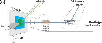
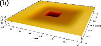
The low energy ion beam is formed by injecting a keV ion beam produced by a VG EX05 gun into the TOF spectrometer ion optics, by delivering and focusing the beam at normal incidence to the sample and by decelerating the ions to the desired low impact energy by biasing the target with an appropriate voltage (see Fig.1). The beam defocusing, which accompanies this deceleration, is compensated by changing the voltage of the outlet electrostatic lens called Lens1 19 . The impact energy of this milling beam was set in this study to either 250 or 500 eV, and the ion current was 1 A. This beam was raster scanned over the sample surface by engaging an octupole deflector present in the TOF system ion path (the Shaping Octupole in Fig. 1), so that a square crater of 1.51.5 mm2 (shown in Fig.1 as a blue square) was eroded. The exact size of the crater depends on the deceleration potential of the target, which additionally deflects the beam when it is raster scanned. For example, the ratio of the crater sides between =250 eV and =3 keV equals 1.3; this value was proved both by crater imaging and by SIMION 3D© 32 simulation.
The analytical ion beam, used to probe the sample at various depths, comes from an Atomika WF421 gun pointed at 60∘ incidence with respect to the target normal (Fig.1). This ion beam can be independently tuned, raster scanned, and pulsed. The primary Ar+ ion energy was always 5 keV, and the pulse duration used in the analysis in all the experiments was 200 ns, since mass resolution under these conditions was sufficient. The raster scan size of this ion beam in all the experiments described here was set to a 500500 m2 (the green square in Fig.1). During the TOF MS analysis cycle, the deceleration potential on the target is switched off. In the gentleDB depth profiling regime, the Atomika ion beam was only used for analysis. By choosing an appropriate aperture, the primary ion current was set to 30 nA, in order to attenuate the secondary ion signal so that the TOF MS detector is not overwhelmed.
For the two ion beams used in these experiments, parameter was 10-5 18 .
In order to perform the gentleDB depth profiling, we fit the analysis beam raster into the center of the low energy sputtering beam raster. To do this pre-alignment, we used a Faraday cup for ion beam collection and took advantage of available crater imaging capabilities. Crater imaging was done in situ by an optical Schwarzschild-type microscope 19 and the SEM 19 ; 33 or by ex situ optical white light interferometry 34 (Fig.1b).
IV Results and Discussion
Figure 2 demonstrates normalized depth profiles obtained by the gentleDB approach at 250 and 500 eV sputtering beam energies. Both the 24Mg and 64Zn depth profiles are very similar and feature high contrast and high stability of the signal all the way through the multilayer structure. The model structure of the 24Mg distribution based on ellipsometry measurements is shown in Fig.2 as a black dotted line. The end of the last layer depth profile is marked by a 28Si signal spike from the substrate. The variation in the 28Si SIMS signal is due to variation in the Si secondary ion yield from SiO2, and its following drop and stabilization are observed at the 100-fold lower level with respect to the spike magnitude, which coincides with the known ratio . The first peak in the 24Mg profile has an unsymmetrical shape (cotangent-like) starting at the surface from the highest SIMS intensities transforming right into trailing edge, while the 64Zn profile starts approximately at the zero level; both profiles then have a steady sine-like shape. Table I shows the leading and decay lengths extracted from the depth profiles. The definition for the leading or decay length is the inverse of the first order coefficient for the linear approximation of the leading or trailing edges of a peak represented in semi-log scale, (Intensity) vs. depth 35 . Here, both and are 5 nm for 24Mg, 2 nm for 64Zn, and =0.4 nm for 28Si. The measured leading and decay lengths were on the same order or better than published to-date corresponding data obtained with commercial state-of-the-art SIMS instrumentation using cluster/molecular or low energy O/Cs+ ion sources, or with laser-assisted atom probe tomography 9 ; 10 ; 12 ; 13 ; 17 ; 36 ; 37 .
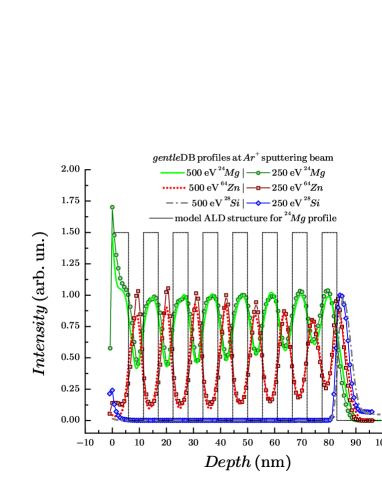
Table I. Leading and decay lengths for 24Mg, 64Zn, and 28Si extracted from gentleDB depth profiles. 500 eV 250 eV (nm) 24Mg 64Zn 28Si 24Mg 64Zn 28Si Average 5.6 2.1 – 4.9 2.2 – Average 5.1 2.1 – 4.7 2.0 – at Si interface 1.3 1.1 – 0.9 0.8 – Si – – 0.4 – – 0.4
As mentioned above, the first 24Mg peak of the stack was not resolved from the surface constituent, which caps the structure. In order to resolve in the depth profile the 24Mg peak corresponding to the topmost ALD layer from the surface contamination, we decreased the time of the individual sputtering cycles and proportionally increased their number. Figure 3 shows the depth profile of the two top layers performed with more data points per depth unit to separate the 24 mass from the topmost layer 24Mg peak. The green line here corresponds to the depth profile with poorer resolved Mg profile, shown in Fig.2. This is to emphasize the capacity in the resolving power tuning of the gentleDB approach. The distance between subsequent depth points in Fig.3 is 0.2 nm, which precisely correlates with half of the average lattice parameter of 3.9 for wurtzite ZnO 38 and half of the cubical unit cell size of crystalline MgO with a lattice parameter of 4.2 39 .
The ratios of 25Mg/24Mg and 26Mg/24Mg proved that the mass 24 peak appears to be Mg with correct terrestrial isotopic ratio values. Such stoichiometry enrichment may be due to either natural surface contamination occurring after the sample is taken out of the ALD reactor, or due to some ALD specific effect manifesting itself at finalizing growth steps. At the same time, the high depth resolution profiling allows us to detect a ”dip” between the surface 24Mg and the topmost magnesia layer so that there is enough prior information to precisely reconstruct the contaminant and MgO layer profiles, assuming the contamination is natural. These two functions are displayed in Fig.3: cyan dotted line corresponds to MgO, while black dotted one is the surface Mg cap.
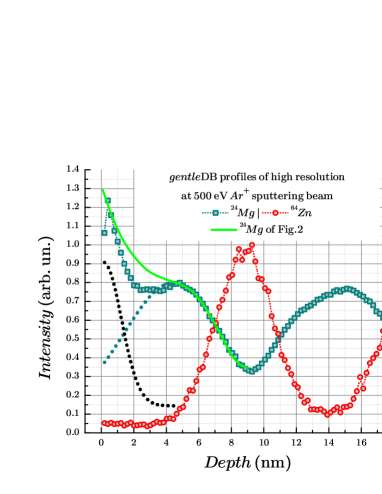
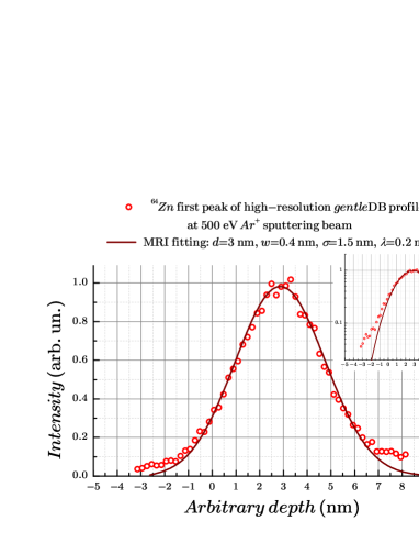
These experimental results clearly demonstrate remarkable resolving power of the gentleDB approach to depth profiling. In this regard, keeping in mind that normal incidence should not affect pronouncedly native sample roughness 20 , let us qualify what the definition ”gentle” means. For this, we apply the MRI (mixing-roughness-information) model 40 ; 41 to simulate the 64Zn peak in the 500 eV high resolution gentleDB depth profiles using the model parameters (cascade mixing length), (r.m.s., root mean square, roughness), and (information depth, or escape depth, 1–2 monolayer in the case of SIMS).
A summary of the MRI model for the SIMS experiment is shown below. Note that the preferential sputtering effect is not taken into account here, since there is no such an effect for MgO and ZnO. As a starting point, the ion mixing is modeled first by the differential equation (1) for an ideal, flat layer of thickness , with the boundary conditions (2), (4), and (5)
Hence,
Hence,
where and are apparent (at any depth ) and actual (at deeper relative to ) concentrations of an element, respectively; is the ion mixing length; and are the flat boundaries of the arbitrary layer of interest, so that equals the layer thickness, . and are the leading and trailing edges of the depth profile peak, respectively. Thus, due to the cascade mixing, the solution yields
If the surface roughness (either inherent, or induced, or both) is taken into account, then the profile additionally broadens as
where the mixing is convolved with the Gaussian function that takes the r.m.s. roughness as the standard deviation.
Finally, when both the parameter and the effective depth contributing to the signal are considered, the depth profile shape can then be expressed as
where is the information depth or ion escape depth, by conventional definition. Generally speaking, in the case of SIMS, it has negligible contribution in the elemental peak dependence on the depth , defined only by the cascade mixing and roughness.
We found that the best matching between the measured and modeled profiles occurs when the MRI parameters and were set as follows: =0.4 nm, =1.5 nm, and the parameter was fixed at value 0.2 nm corresponding to 1 monolayer. The nominal thickness (flat thickness) of the layer, , had to be of 3 nm to get the best peak fit in Fig.4. The thickness is not a free parameter of the MRI model. Nevertheless, being unknown a priori, it had to be varied in order to define the boundary conditions (2), (4), and (5). Then the effective thickness of a single ZnO layer, i.e., 2, equals to 6 nm. This value obtained by MRI does agree well with the ones estimated for a single ALD layer by ellipsometry and quartz crystal microbalance technique except the real material layer is not ideally flat, it can be represented by a structure made of flat inner layer squeezed between comparable in thickness additions on both sides representing wavy interfaces. Thus, under gentleDB conditions, the value =1.5 nm calculated for the first 64Zn peak can be accepted as the native roughness of the sample inner interfaces (see Fig.4). In agreement with the MRI model results, this roughness causes symmetrical peak broadening in sputter depth profiling experiments.
It is interesting, that some preceding works, e.g. Ref.42 , concluded that the attenuation of the signal intensity of each subsequent layer in laminate/multilayer structures, by approximately law, occurs only due to the native interface roughness of layered structures. However, presented here results of the gentleDB depth profiling obtained on a sample of exceedingly disturbed grown interfaces suggest that the native roughness is not the dominant factor in the degradation and smearing of depth profiles in SIMS. To prove this, we applied the conventional single beam TOF SIMS depth profiling approach to the same sample, using 5 keV Ar+ ions with 60∘ incidence angle (generated by the Atomika WF421 ion gun) – for both ion milling and TOF MS analysis (results to be published). The comparison between single beam and gentleDB approaches revealed dramatic differences in results: the ion beam mixing length increased from 0.4 nm to 3 to 4 nm 43 , which is on the order of the entire ALD layer thickness. Moreover, we observed with single beam approach the periodical sine signal with exponential attenuation mentioned above as well as the smearing of the peak shapes for deeper layers. To summarize, the ion beam mixing appears to be the most important phenomenon to account for in depth profiling experiments on nanolayered structures. Reducing ion mixing length by a proper choice of the analytical procedure can produce depth profiles such as the ones shown in Fig.2 that reveal much more information about the samples than about the measurement artifacts/distortions.
V Conclusion
To conclude, we have outlined here our approach to solve the nanomaterial characterization bottleneck problem 22 in the materials science by application of TOF SIMS technique. Namely, we described our gentle variant of the dual-beam sputter depth profiling (gentleDB) applied to characterization of nanolayered materials and demonstrated sub-nanometer depth resolution of the method. This approach combines normally incident low energy (down to sputtering threshold) Ar+ ion beam for sputtering with several keV pulsed Ar+ ion beam (60∘ incidence angle) for analysis. The shallow penetration depth of these sputtering primary ions results in an ultra-short range of a crystal lattice disturbance of about 0.4 nm thus enabling measurements of structural parameters (flat thickness and roughness) of a stack of 16 alternating MgO and ZnO nanolayers (8 of each, with thickness of 5.5 nm) grown by ALD on a Si substrate. The interfacial roughness as small as 1.5 nm estimated by the gentleDB sputter depth profiling does agree well with measurements obtained by other techniques: the surface roughness of individual ZnO layers (0.5 nm) determined by atomic force microscopy 30 and the roughness of the multilayer structure (0.9-1.5 nm) as determined by x-ray reflectivity and atomic force microscopy for comparable ALD-grown Al2O3/ZnO multilayers 24 ; 30 .
Acknowledgements. This work was supported under Contract No. DE-AC02-06CH11357 between UChicago Argonne, LLC and the U.S. Department of Energy and by NASA through grants NNH08AH761 and NNH08ZDA001N.
References
- (1) O. Ingolfsson and A. M. Wodtke, Phys. Rev. Lett. 87, 183401 (2001).
- (2) R. J. H. Morris and M. G. Dowsett, J. Appl. Phys. 105, 114316 (2009).
- (3) N. Vanhove, P. Lievens and W. Vandervorst, Phys. Rev. B 79, 035305 (2009).
- (4) H. Oechsner, R. Getto and M. Kopnarski, J. Appl. Phys. 105, 063523 (2009).
- (5) A. Lakatos, G. A. Langer, A. Csik, C. Cserhati, M. Kis-Varga, L. Daroczi, G. L. Katona, Z. Erdelyi, G. Erdelyi, K. Vad and D. L. Beke, Appl. Phys. Lett. 97, 233103 (2010).
- (6) M. P. Seah, C. P. A. Mulcahy and S. Biswas, J. Vac. Sci. Technol. B 28, 1215 (2010).
- (7) G. Betz and G. K. Wehner, Topics in Applied Physics 52, 11 (1983).
- (8) M. Nastasi and J. W. Mayer, Materials Science and Engineering R: Reports 12, 1 (1994).
- (9) S. Koelling, M. Gilbert, J. Goossens, A. Hikavyy, O. Richard and W. Vandervorst, Appl. Phys. Lett. 95, 144106 (2009).
- (10) Y. Shimizu, Y. Kawamura, M. Uematsu, M. Tomita, T. Kinno, N. Okada, M. Kato, H. Uchida, M. Takahashi, H. Ito, H. Ishikawa, Y. Ohji, H. Takamizawa, Y. Nagai and K. M. Itoh, J. Appl. Phys. 109, 036102 (2011).
- (11) M. G. Dowsett, N. S. Smith, R. Bridgeland, D. Richards, A. C. Lovejoy and P. Pedrick, Secondary ion mass spectrometry SIMS X: proceedings of the Tenth International Conference on Secondary Ion Mass Spectrometry, Eds. A. Benninghoven, B. Hagenhoff, and H. W. Werner, p.367. Wiley, Chichester (1997).
- (12) A. Chanbasha and A. Wee, Appl. Surf. Sci. 255, 1307 (2008).
- (13) K. Iltgen, A. Benninghoven and E. Niehuis, Secondary ion mass spectrometry SIMS XI: proceedings of the Eleventh International Conference on Secondary Ion Mass Spectrometry, Eds. G. Gillen, R. Lareau, J. Bennett, and F. Stevie, p.367. Wiley, Chichester (1998).
- (14) N. Winograd, Anal. Chem. 77, A142 (2005).
- (15) D. Touboul, F. Kollmer, E. Niehuis, A. Brunelle and O. Laprevote, J. Am. Soc. Mass Specrom. 16, 1608 (2005).
- (16) I. Yamada, J. Matsuo, N. Toyoda and A. Kirkpatrick, Materials Science and Engineering: R: Reports 34, 231 (2001).
- (17) K. Iltgen, C. Bendel, A. Benninghoven and E. Niehuis, J. Vac. Sci. Technol. A 15, 460 (1997).
- (18) The depth resolution is controlled only by the sputtering beam parameters as long as the parameter . We introduce here the parameter for accurate comparison of ion sources with different operating currents, beam energies, and primary species types . The parameter can be called here the effective erosion efficiency () of an ion source (in [at/cm2]) at a specific current density and sputtering yield , that depends on sputtering species and their energy , where denotes element or material under sputtering , where is the elementary charge and is the time interval when an ion gun is on during a single sputtering or analysis cycle. One can compare this strict parameter with simple ratio of current densities proposed in K. Iltgen et al, J. Vac. Sci. Technol. A 15, 460 (1997).
- (19) I. Veryovkin, C. E. Tripa and M. Pellin, Physics Procedia 1, 379 (2008).
- (20) T. J. Ormsby, D. P. Chu, M. G. Dowsett, G. A. Cooke and S. B. Patel, Appl. Surf. Sci. 144-145, 292 (1999).
- (21) I. V. Veryovkin, C. E. Tripa, A. V. Zinovev, S. V. Baryshev, M. J. Pellin and D. S. Burnett, 42nd Lunar and Planetary Science Conference, Abstract 2308 (2011).
- (22) E. K. Richman and J. E. Hutchison, ACS Nano 3, 2441 (2009).
- (23) E. Thimsen, Q. Peng, A. B. F. Martinson, M. J. Pellin and J. W. Elam, Chem. Mater. 23, 4411 (2011).
- (24) J. M. Jensen, A. B. Oelkers, R. Toivola, D. C. Johnson, J. W. Elam and S. M. George, Chem. Mater. 14, 2276 (2002).
- (25) A. U. Mane, Q. Peng, M. J. Wetstein, R. G. Wagner, H. J. Frisch, O. H. W. Siegmund, M. J. Minot, B. W. Adams, M. C. Chollet and J. W. Elam, Proc. SPIE 8031, 80312H (2011).
- (26) I. Bakonyi and L. Peter, Progress in Materials Science 55, 107 (2010).
- (27) J. M. Rondinelli and N. A. Spaldin, Adv. Mater. 23, 3363 (2011).
- (28) V. Lujala, J. Skarp, M. Tammenmaa and T. Suntola, Appl. Surf. Sci. 82-83, 34 (1994).
- (29) M. Putkonen, T. Sajavaara and L. Niinisto, J. Mater. Chem. 10, 1857 (2000).
- (30) J. W. Elam, Z. A. Sechrista and S. M. George, Thin Solid Films 414, 43 (2002).
- (31) I. Veryovkin, W. Calaway and M. Pellin, Nucl. Instrum. Methods Phys. Res. A 519, 353 (2004).
- (32) Scientific Instrument Services, Inc., SIMION software (http://www.simion.com/).
- (33) S. V. Baryshev, A. V. Zinovev, C. E. Tripa, M. J. Pellin, D. S. Burnett and I. V. Veryovkin, 43nd Lunar and Planetary Science Conference, Abstract 2909 (2012).
- (34) S. V. Baryshev, A. V. Zinovev, C. E. Tripa, R. A. Erck and I. V. Veryovkin, Appl. Surf. Sci. (2012). DOI:10.1016/j.apsusc.2012.03.144 / arXiv:1204.0808v1
- (35) K. Wittmaack, Nucl. Instrum. Methods Phys. Res. 209/210, 191 (1983).
- (36) M. J. P. Hopstaken, M. S. Gordon, D. Pfeiffer, D. K. Sadana, T. Topuria, P. M. Rice, C. Gerl, M. Richter and C. Marchiori, J. Vac. Sci. Technol. B 28, 1287 (2010).
- (37) M. G. Dowsett and D. P. Chu, J. Vac. Sci. Technol. B 16, 377 (1998).
- (38) H. Sowa and H. Ahsbahs, J. Appl. Cryst. 39, 169 (2006).
- (39) W.-Y. Hsu and R. Raj, Appl. Phys. Lett. 60, 3105 (1992).
- (40) S. Hofmann, J. Vac. Sci. Technol. B 10, 316 (1992).
- (41) S. Hofmann, Surf. Interface Anal. 21, 673 (1994).
- (42) A. Bartok, A. Csik, K. Vad, G. Molnar, E. Toth-Kadar and L. Peter, Journal of The Electrochemical Society 156, D253 (2009).
- (43) S. Hofmann, Rep. Prog. Phys. 61, 827 (1998).