Intrinsic Terahertz Plasmons and Magnetoplasmons in Large Scale Monolayer Graphene
Abstract
We show that in graphene epitaxially grown on SiC the Drude absorption is transformed into a strong terahertz plasmonic peak due to natural nanoscale inhomogeneities, such as substrate terraces and wrinkles. The excitation of the plasmon modifies dramatically the magneto-optical response and in particular the Faraday rotation. This makes graphene a unique playground for plasmon-controlled magneto-optical phenomena thanks to a cyclotron mass 2 orders of magnitude smaller than in conventional plasmonic materials such as noble metals.
Graphene attracts a lot of attention as a novel optoelectronic and plasmonic material for applications ranging from the terahertz to the visibleWunschNJP06 ; HwangPRB07 ; MikhailovPRL07 ; RanaIEEE08 ; JablanPRB08 ; XiaNatureNanoTech09 ; BonaccorsoNaturePhoton10 ; BludovEPL10 ; EchtermeyerNatureComm11 ; JuNatureNano11 ; KoppensNanoLett11 ; FeiNanoLett11 ; EnghetaScience11 ; NikitinPRB11 . One expects that plasmon waves in graphene can be squeezed into a much smaller volumeKoppensNanoLett11 ; EnghetaScience11 than in noble metals routinely used in plasmonics and, importantly, can be manipulated by external gate voltage. A Dirac-like linear electronic dispersion and zero bandgap in graphene make its electromagnetic response rather unusual compared to other known two-dimensional conductors, such as 2D electron gases (2DEGs) in semiconductor heterostructuresAndoRevModPhys82 , even though the basic description of the propagating plasma modes is essentially the sameWunschNJP06 ; HwangPRB07 .
In order to observe plasmonic absorption optically one generally has to break the translational invariance of the system. Typical ways to couple plasmons to electromagnetic radiation in two-dimensional systems are placing an external grid in the vicinity of the sampleAllenPRL77 and making stripe- or dotlike periodic structures inside the systemAllenPRB83 ; HeitmannSurfSci92 ; KukushkinPRL03 . In graphene, this coupling has recently been achieved by pattering it in the shape of ribbonsJuNatureNano11 and by using a metallic atomic force microscopy (AFM) tip in scattering-type scanning near field optical microscopyFeiNanoLett11 . However, no measurement of graphene plasmons in magnetic field was reported so far.
Graphene epitaxially grown on SiC shows a number of intrinsic uniformly distributed defects caused by the substrate terraces and thermal relaxation after the graphitization processCambazCarbon08 ; EmtsevNatureMat09 ; CamaraPRB09 ; FortiPRB11 . In this Letter, we demonstrate that these defects, usually considered a nuisance, are in fact beneficial to excite terahertz plasmons in graphene without the need for artificial structuring. Because of the small cyclotron mass of the Dirac-like charge carriers in graphene we observe a strong effect of the magnetic field on the plasma modes, reminiscent of the behavior observed in 2DEGs. This is in drastic contrast to conventional plasmonic materials like gold, where the carrier mass exceeds the free-electron mass, leading to at best a weak dependence on magnetic fieldSepulvedaPRL10 .
A layer of honeycomb carbon was grown on the silicon side of SiC by a graphitization procedure at 1450 ∘C in an Argon atmosphere, as described in our previous workCrasseeNatPhys11 . Subsequent hydrogen passivation of the silicon dangling bonds transformed the so-called buffer layer into quasi freestanding grapheneRiedlPRL09 ; SpeckMatSciForum10 . X-ray photoemission spectroscopy confirmed that the thickness was one graphene layer and that the backside of the SiC substrate was graphene free. After hydrogenation, graphene becomes strongly p-doped; the Fermi level, -0.34 eV, is below the Dirac point, which corresponds to a hole concentration cm-2CrasseeNatPhys11 , where m/s is the Fermi velocity. All magneto-optical measurements were done in the Faraday geometry (magnetic field and propagation of light normal to the sample) using a Fourier transform infrared spectrometer connected to a split-coil superconducting magnetCrasseeNatPhys11 . The illuminated area of several square millimeters was fully covered by graphene.
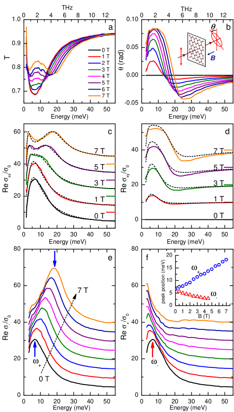
Figures 1a,b show the optical transmission and Faraday rotation spectra measured at 5 K in fields up to 7 T. The diagonal conductivity , normalized to the universal conductivity AndoJPSJ02 , shown in Figure 1c is obtained from the optical transmission, as described in the Supporting Information. At zero magnetic field, we observe a strong maximum centered around 6.5 meV (1.6 THz) instead of the normally expected Drude peak at zero frequency due to free carriers. As we demonstrate below, the deviation from the Drude behavior is associated with the presence of a confinement potential acting on free carriers and the corresponding plasmonic absorption. A similar resonance was observed recently in graphene micro-ribbons in the polarization perpendicular to the ribbonsJuNatureNano11 .
When a magnetic field is applied, the plasma resonance splits into two modes, one of which increases and the other decreases with (Figure 1c). In order to get further insight into the origin of these modes we extracted the Hall conductivity from the Faraday rotation spectra (Figure 1d) and obtained the optical conductivity for left and right circularly polarized radiation, (Figures 1e,f), as described in the Supporting Information. One can clearly see that each of the modes is excited only in one circular polarization. The peak positions in and we denote and respectively, since the former increases and the latter decreases with magnetic field. The inset of Figure 1f shows the field dependence of and . The field-induced splitting of the plasmon peak resembles strikingly the appearance of collective resonances observed previously in disk-shaped quantum dots of two-dimensional electron gases based on GaAs heterostructures AllenPRB83 ; KukushkinPRL03 and in bound 2D electrons on the surface of liquid helium MastPRL85 ; GlattiPRL85 . In both cases, the upper and lower branches were attributed to the so-called bulk and edge magnetoplasmons, respectively, with the frequenciesAllenPRB83
| (1) |
where is the plasmon frequency at zero field, is the cyclotron frequency, defined as positive for electrons and negative for holes, is the cyclotron mass, and the speed of light. At high fields (), the upper branch becomes essentially the usual cyclotron resonance with a linear dependence on magnetic field, while the lower branch represents a collective mode confined to the edgesFetterPRB85 with the energy inversely proportional to the field.
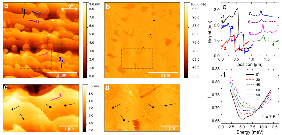
In order to clarify the origin of the confinement that causes the plasmonic resonance, we performed vibrating cantilever AFM imaging, allowing us to extract topographic and phase information. In Figure 2a a topographical height image of a 10 10 m2 area of the sample is presented. The dominating structures are the terraces due to the miscut angle of SiC. Their irregular shape as compared to morphologies observed earlier EmtsevNatureMat09 is related to the specific graphitization temperature used in our work. Importantly, the terraces are oriented in the same direction across the entire sample. Figure 2b presents the map of the oscillation phase of the cantilever on the same area. The dark spots in the phase correspond to regions without graphene, as was determined by Raman spectroscopy. Closer inspection of the AFM images also reveals numerous wrinkles such as the ones indicated by the arrows in Figures 2c,d. The wrinkles are formed due to the relaxation of strain in graphene during the cooling down after the graphitizationCambazCarbon08 . Figure 2e shows height profiles for the lines marked in Figure 2a. Profiles 1 to 3 correspond to steps in the SiC substrate, while traces 4 to 7 are taken across the wrinkles on the terraces and show that these wrinkles have a height of less than 1 nm, which is in agreement with previous workCambazCarbon08 . The regions of homogeneous graphene have a typical size of about one micrometer throughout the whole sample.
Polarized optical transmission (Figure 2f) provides a hint that the terahertz resonance peak is related to the morphological structures seen by AFM. A significant anisotropy is found, which correlates with the orientation of the terraces. In particular, the absorption maximum is at about 1.7 times higher energy for the electric field perpendicular to the terraces than for the parallel orientation. Note that the peak position remains at finite energy for every polarization. The excitation of the plasmon parallel to the terraces is likely due to the rough shape of the SiC step edges. One cannot exclude that the wrinkles, which are randomly oriented, might also play a role in confining the carriers. Because of the anisotropy, the curves and the plasmon energy in Figure 1 are effective averages over all polarizations.
It is worthwhile to notice that the terahertz transmission of multilayer graphene epitaxially grown on the carbon side of SiC also reveals an absorption peak, although at a somewhat lower energy, with a strong polarization dependence as shown in the Supporting Information. Although it might have a similar plasmon origin as in the case of monolayer graphene on the silicon face of SiC, the presence of many layers with different doping levels makes this interpretation less straightforward.
We found that it is possible to describe quantitatively the plasmon structure and its splitting in magnetic field by a Drude-Lorentz formula for the optical conductivityAllenPRB83 ; MikhailovPRB96 :
| (2) |
where is the plasmon spectral weight and is the scattering rate. In the present case, this equation should be regarded as purely phenomenological, although it can be rigorously derived for certain types of inhomogeneous media, such as disk-shaped quantum dots, using the effective medium Maxwell-Garnett approach (the relevant details are given in the Supporting Information). Equation 8 is the simplest analytical expression which reduces to a Lorentzian shape in the limit of zero field () and describes the usual Drude cyclotron resonance when the plasmon energy is vanishing (). For small values of , it indeed has resonances at frequencies given by eq. 1. We fitted the experimental spectra of both and at every magnetic field to eq. 8, treating , , and as adjustable parameters. We also added a small frequency independent background term 3.5 to the real part of the diagonal optical conductivity, which may have various origins, as discussed in the Supporting Information. The fits are shown as dashed lines in Figures 1c,d. The experimental data including all important spectral features are well reproduced, which, given the complexity of the sample, comes as an encouraging surprise to be explained in future studies. However, the noticeable deviations, especially in , demonstrate the limitations of this simple model with respect to our sample.
Figure 3 shows the field dependence of and extracted from the fitting procedure. The bare plasmon frequency is essentially constant, while the cyclotron frequency demonstrates a nearly perfectly linear growth with a slope = 2.1 meV/T corresponding to a cyclotron mass of 5.5 % of the free electron mass . Note that in our previous workCrasseeNatPhys11 an apparent deviation from the linear dependence was reported because the plasmonic contribution was not taken into account. In Figure 3, we also plot the magnetoplasmon frequencies calculated using eq. 1 and the experimental values of and . They are very close to the peak positions in (Figure 1e,f). The spectral weight of the plasmon peak shows only a small, if any, magnetic field dependence. The value of extracted from the fitting is about 0.52 eV. Taken alone, it is somewhat smaller than the expected value of — = 0.68 eV. The difference might be related to a noncomplete coverage of the substrate by graphene (see Figure 2b), however can also be due to the presence of the background . The broadening, , of the peak is about 10-12 meV, which is more than two times smaller than observed in a similar sample by another groupYanACSNano . It might still be larger than the intrinsic electron scattering, since the spectral feature is additionally broadened by the distribution of sizes and shapes of the homogeneous regions. A more detailed discussion of the spectral weight, background, and scattering is given in the Supporting Information.
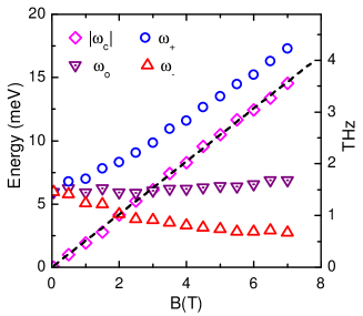
The Dirac-like charge carriers in graphene at high doping are expected to show a classical cyclotron resonance with a linear dependence on magnetic fieldAndoJPSJ02 , which perfectly agrees with our data. The cyclotron mass depends on doping according to the relation . Using 0.34 eV, and 0.055 , we find that 1.04 106 m/s, which matches remarkably well the Fermi velocity obtained by other methodsOrlitaSemiSciTech10 .
The plasmon frequency, 6.5 meV, contains important information about the intrinsic properties of the electron gas and the confinement causing the plasmon excitation. It is instructive to compare the value of found in this work with the resonant frequency for the reference case of isolated disk-shaped quantum dots, for which the effective medium model predictsAllenPRB83 ; LeavittPRB86 ; MikhailovPRB96 :
| (3) |
where is the average dielectric constant of the surrounding media and is the dot diameter. For m, which roughly corresponds to the mean size of homogeneous regions in our sample, and for the same charge density cm-2, the expected plasmon frequency would be 15.2 meV. This is more than twice the experimentally observed value. Lacking a rigorous quantitative model for the present sample, we ascribe this difference to the fact that the defect lines that separate homogeneous graphene regions are very narrow, and that the electromagnetic coupling between neighboring regions therefore plays an important role. Such a coupling causes a redshiftMikhailovPRB96 ; RomeroOpticsexpress06 ; LassiterNanoLett08 ; NikitinArxiv11 of the plasmon energy as compared to the case of noncoupled particles, which is commonly observed in plasmonic nanostructures.
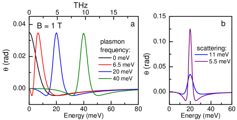
Important for terahertz applications is the question to what extent the presence of a plasmon affects the Faraday rotation in graphene. The simulations in Figure 4a demonstrate that the Faraday angle is at maximum close to the magnetoplasmon resonance and therefore can be controlled not only by magnetic field but also by . Here we compare the calculated Faraday rotation of homogeneous graphene ( 0) and the rotation in the presence of plasmons such as the one observed in our sample (6.5 meV) and for higher plasmon energies (20 and 40 meV). A way to increase the plasmon frequency is to decrease the size of the homogeneous regions, which could be done, for example, by varying the miscut angle of the substrate. Notice that a route to increase the Faraday rotation for a given plasmon frequency is to use samples with reduced electronic scattering as demonstrated in Figure 4b. Rotations above 0.1 radians by just one atomic layer at a modest field of 1 T do not seem to be out of experimental reach.
Similarly, in more conventional plasmonic materials the Faraday and Kerr angles are enhanced close to the plasma resonanceSepulvedaPRL10 ; BonanniNanoLett11 . For example, in a recent work a Kerr rotation on the order of 10-4 to 10-3 radians was detected in an array of Au disksSepulvedaPRL10 . Thus, graphene shows more than 2 orders of magnitude larger rotation, which is a direct consequence of a much smaller cyclotron mass even though the carrier density per unit cell is also much lower than in noble metals. The measurements presented in this Letter were performed at low temperature to maximally resolve the magnetoplasmonic spectral structures. We do believe, though, that the magnetoplasmonic phenomena described here will persist up to room temperature, based on our temperature dependent experimental study of the cyclotron resonance in epitaxial graphene on the carbon face of SiCCrasseePRB11 .
In conclusion, we found that morphological defects on the nanoscale such as atomic steps in SiC and wrinkles in epitaxial graphene produce a remarkably strong plasmon resonance. This resonance has essentially the same origin as the plasmon peak observed in two-dimensional electron gases and in nanostructured graphene. The important difference, however, is that the confinement potential in epitaxial graphene is natural and does not require special lithographic patterning, which risks reducing the carrier mobility. Instead, one can think of controlling the plasmon frequency by varying the preparation of the substrate and the graphitization process. The presence of the plasmon dramatically changes the cyclotron resonance and Faraday rotation. Graphene appears to be a unique material, where one finds simultaneously a small effective mass giving rise to strong magneto-optical effects and excellent plasmonic properties. This combination opens pathways toward plasmon-controlled terahertz magneto-optics.
After the submission of this paper we became aware of the work by H. Yan et al.YanNatNano12 ; YanArxiv12 , which reports the observation of plasmons and magnetoplasmons in micron sized graphene disks.
This work was supported by the Swiss National Science Foundation (SNSF) by Grants 200021-120347 and IZ73Z0-128026 (SCOPES program), through the National Centre of Competence in Research “Materials with Novel Electronic Properties-MaNEP” and by projects EuromagnetII, GACR P204/10/1020 and GRA/10/E006 (Eurographene-EPIGRAT) and the ESF Eurographene project “Graphic-RF”. We thank R. Hillenbrand, S. A. Mikhailov, and D. van der Marel for useful discussions.
References
- (1) Wunsch, B.; Stauber, T.; Sols, F.; Guinea, F. New J. Phys. 2006, 8, 318.
- (2) Hwang, E. H.; Das Sarma, S. Phys. Rev. B 2006, 75, 205418.
- (3) Mikhailov, S. A.; Ziegler, K. Phys. Rev. Lett. 2007, 99, 016803.
- (4) Rana, F. IEEE Trans. Nanotechnol. 2008, 7, 91-99.
- (5) Jablan, M.; Buljan, H.; Soljai, M. Phys. Rev. B 2008, 80, 245435.
- (6) Xia, F.; Mueller, T.; Lin, Y. -M.; Valdes-Garcia, A.; Avouris, P. Nat. nanotechnol. 2009, 4, 839-843.
- (7) Bonaccorso, F.; Sun, Z.; Hasan, T.; Ferrari, C. Nat. Photonics 2010, 4, 611-622.
- (8) Bludov, Yu. V.; Vasilevskiy, M. I.; Peres, N. M. R. EPL 2010, 92, 68001.
- (9) Echtermeyer, T. J.; Britnell, L.; Jasnos, P. K.; Lombardo, A.; Gorbachev, R. V.; Grigorenko, A. N.; Geim, A. K.; Ferrari, A. C.; Novoselov, K. S. Nat. Commun. 2011, 2, 458.
- (10) Ju, L.; Geng, B.; Horng, J.; Girit, C.; Martin, M.; Hao, Z.; Bechtel, H. A.; Liang, X.; Zettl, A.; Shen, Y. R.; Wang, F. Nat. Nanotechnol. 2011, 6, 630-634.
- (11) Koppens, F. H. L.; Chang, D. E.; Garcia de Abajo, F. J. Nano Lett. 2011, 11, 3370-3377.
- (12) Fei, Z.; Andreev, G. O.; Bao, W.; Zhang, L. M.; McLeod, A. S.; Wang, C.; Stewart, M. K.; Zhao, Z.; Dominguez, G.; Thiemens, M.; Fogler, M. M.; Tauber, M. J.; Castro-Neto, A. H.; Ning Lau, C.; Keilmann, F.; Basov, D. N. Nano Lett. 2011, 11, 4701-4705.
- (13) Vakil, A.; Engheta, N. Science 2011, 332, 1291-1294.
- (14) Nikitin, A. Y.; Guinea, F.; Garcia-Vidal, F.; Martin-Moreno, L. Phys. Rev. B 2011, 84, 195446.
- (15) Ando, T.; Fowler, A. B.; Stern, F. Rev. Mod. Phys. 1982, 54, 437-672.
- (16) Allen, S. J.; Tsui, D. C.; Logan, R. A. Phys. Rev. Lett. 1977, 38, 980-983.
- (17) Allen, S. J.; Stormer, H. L.; Hwang, J. C. M. Phys. Rev. B 1983, 28, 4875-4877.
- (18) Heitmann, D; Kern, K; Demel, T; Grambow, P; Ploog, K; Zhang, Y Surf. Sci. 1992, 267, 245.
- (19) Kukushkin, I. V.; Smet, J. H.; Mikhailov, S. A.; Kulakovskii, D. V.; von Klitzing, K.; Wegscheider, W. Phys. Rev. Lett. 2003, 90, 156801.
- (20) Goknur Cambaz, Z.; Yushin, G.; Osswald, S.; Mochalin, V.; Gogotsi, Y. Carbon 2008, 46, 841-849.
- (21) Forti, S.; Emtsev, K. V.; Coletti, C.; Zakharov, A. A.; Riedl, C.; Starke, U. Phys. Rev. B 2011, 84, 125449.
- (22) Camara, N.; Huntzinger, J.-R.; Rius, G.; Tiber, A.; Mestres, N.; P rez-Murano, F.; Godignon, P.; Camassel, J. Phys. Rev. B 2009, 80, 125410.
- (23) Emtsev, K. V.; Bostwick, A.; Horn, K.; Jobst, J.; Kellogg, G. L.; Ley, L.; McChesney, J. L.; Ohta, T.; Reshanov, S. A.; Röhrl, J.; Rotenberg, E.; Schmid, A. K.; Waldmann, D.; Weber, H. B.; Seyller, Th. Nat. Mater. 2009, 8, 203-207.
- (24) Sep lveda, B.; Gonz lez-D az, J. B.; Garc a-Mart n, A.; Lechuga, L. M.; Armelles, G. Phys. Rev. Lett. 2010, 104, 147401.
- (25) Crassee, I.; Levallois, J.; Walter, A. L.; Ostler, M.; Bostwick, A.; Rotenberg, E.; Seyller, Th.; van der Marel, D.; Kuzmenko, A. B. Nat. Phys. 2011, 7, 48-51.
- (26) Riedl, C.; Coletti, C.; Iwasaki, T.; Zakharov, A. A.; Starke, U. Phys. Rev. Lett. 2009, 103, 246804.
- (27) Speck, F.; Ostler, M.; Röhrl, J.; Jobst, J.; Waldmann, D.; Hundhausen, M.; Ley, L.; Weber, H. B.; Seyller, Th. Mater. Sci. Forum 2010, 645, 629-632.
- (28) Ando, T.; Zheng, Y.; Suzuura, H. J. Phys. Soc. Jpn. 2002, 71, 1318-1324.
- (29) Mast, D. B.; Dahm, A. J.; Fetter, A. L. Phys. Rev. Lett. 1985, 54, 1706-1709.
- (30) Glattli, D. C.; Andrei, E. Y.; Deville, G.; Poitrenaud, J.; Williams, F. I. B. Phys. Rev. Lett. 1985, 54, 1710-1713.
- (31) Fetter, A. L. Phys. Rev. B 1985, 32, 7676-7684.
- (32) Mikhailov, S. A. Phys. Rev. B 1996, 54, 10335-10338.
- (33) Yan, H.; F. Xia, F.; Zhu, W.; Freitag, M.; Dimitrakopoulos, C.; Bol, A. A.; Tulevski, G.; Avouris, P. ACS Nano 2011, 5, 9854-9860.
- (34) Orlita, M.; Potemski, M. Semicond. Sci. Technol. 2010, 25, 063001.
- (35) Leavitt R. P.; Little, J. W. Phys. Rev. B 1986, 34, 2450-2457.
- (36) Romero, I.; Aizpurua, J.; Bryant, G. W.; Garc a De Abajo, F. J. Opt. Express 2006, 14, 9988-9999.
- (37) Lassiter, J. B.; Aizpurua, J; Hernandez, L. I.; Brandl, D. W.; Romero, I.; Lal, S.; Hafner, J. H.; Nordlander, P.; Halas, N. J. Nano Lett. 2008, 8, 1212-1218.
- (38) Nikitin, A. Y.; Guinea, F.; Garcia-Vidal, F. J.; Martin-Moreno, L. Phys Rev B 2012, 85, 081405.
- (39) Bonanni, V.; Bonetti, S.; Pakizeh, T.; Pirzadeh, Z.; Chen, J.; Nogu s, J.; Vavassori, P.; Hillenbrand, R.; kerman, J.; Dmitriev A. Nano Lett. 2011, 11, 5333-5338.
- (40) Crassee, I.; Levallois, J.; van der Marel, D.; Walter, A. L.; Seyller, Th.; Kuzmenko, A. B. Phys. Rev. B 2011, 84, 035103.
- (41) Yan, H.; Li, X.; Chandra, B.; Tulevski, G.; Wu, Y.; Freitag, M.; Zhu, W.; Avouris, P.; Xia, F. Nat. nanotechnol. 2012, doi:10.1038/nnano.2012.59
- (42) Yan, H.; Li, Z.; Li, X.; Zhu, W.; Avouris, P.; Xia, F. ArXiv: 1204.4398, 2012
Supporting Information
.1 Extraction of the optical conductivity components from transmission and Faraday rotation spectra
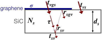
In deriving the relations between the optical conductivity of graphene and the measured spectra, we must take into account multiple reflections in the substrate, which is partially transparent in the considered spectral range. One can do the standard plane-wave counting in the “vacuum () / graphene () / substrate () / vacuum ()” system using the complex coefficients (Figure 1):
| (1) |
Here and are the experimentally known complex refractive index and the thickness of the substrate, = 377 is the impedance of vacuum and is the two-dimensional optical conductivity of graphene. In our measurements the spectral resolution was reduced to 5 cm-1 in order to suppress the Fabry-Perot interference. In this case the multiple reflected rays add incoherently (i.e. by power and not by electric field), and the experimental transmission coefficients of the bare substrate and the sample are given by:
| (2) |
which results in the substrate-normalized transmission:
| (3) | |||||
Since in the transparency window of the substrate, one can safely neglect in all complex coefficients (eq. 1), except in . Defining the absorption coefficient of the substrate and the substrate-vacuum amplitude reflectivity we arrive, after some algebra, at the relation:
| (4) |
In principle, the power transmission alone is not sufficient to determine the complex conductivity . However, the prefactor in the second term is much larger than the one in the third term, therefore the imaginary part of affects the transmission much less than the real part. Under these circumstances a reasonable approximation is to invert the above equation with respect to by setting to zero. In magnetic field, eq. 4 remains strictly valid for each circular polarization separately, if one substitutes with . In unpolarized light, however, the transmission is an average of the two. In order to extract the diagonal conductivity shown in Figure 1c of the main text, we made a further simplification by ignoring the relatively small effect of on the transmission and substituting with in eq. 4.
Likewise, the Faraday rotation is effectively averaged over different internal reflections in the substrate. Experimentally, the Faraday angle is determined from the position of the minimum in the optical signal as a function of the relative angle between two polarizers set before and after the sample. Adding the substrate reflections incoherently, we obtain the exact expression:
| (5) |
where and are obtained from eq. 1 by substituting . Although the Faraday angle is a function of all components of the optical conductivity tensor, we found that for the relevant parameter values the simple linear approximation holds:
| (6) |
This allows us to determine the real part of the Hall conductivity (Figure 1d of the main text) directly from the Faraday angle. In order to extract the real part of , shown in Figures 1e and 1f of the main text, the imaginary part of has to be determined as well. For this purpose we used the Kramers-Kronig relations for , using the model curves to extrapolate data beyond the experimental range.
.2 Polarization dependent transmission of multilayer graphene on the carbon side of SiC
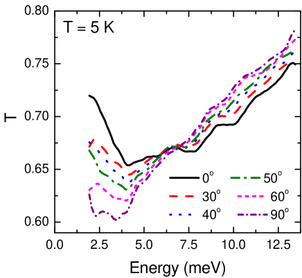
The THz transmission spectra of multilayer graphene epitaxially grown on the carbon side of SiC are shown in Figure 2 for different polarizations at 5 K and 0 T. The sample has 4 to 6 rotationally stacked layers. Two observations can be made: (i) the spectra are strongly polarization dependent and (ii) there is a transmission dip (absorption peak) between 3 and 5 meV depending on the polarization. Therefore this sample also shows a clear deviation from the Drude behavior at low enough frequencies, similar to graphene on the silicon face of SiC discussed in the main text. The peak energy for the carbon-side graphene is lower than for the Si-face graphene. At this stage it is premature to speculate from which graphene layers (the highly doped layer close to the substrate or nearly undoped top layers) this peak stems and to conclude on its physical origin.
.3 Effective medium approximation for isolated disk-shaped quantum dots
The effective medium approximation is a standard approach to calculate optical properties of inhomogeneous media. In the case of isolated quantum dots of a two dimensional electron gas, the Maxwell-Garnett effective medium model results in the following relationAllenPRB83S :
| (7) |
Here is the intrinsic conductivity of the electron gas, is the average dielectric function of the surrounding media, is the filling factor, is the dot diameter and is a geometrical parameter related to the depolarization factor of the dots. For the circular shape, the exact value for is LeavittPRB86S ; MikhailovPRB96S .
The optical conductivity of a homogeneous 2D electron gas or of highly doped graphene in magnetic field, assuming constant scattering, is given by:
| (8) |
where is the density, is the mass, is the cyclotron frequency and is the scattering rate of the charge carriers. Using eq. 7, we obtain the following effective conductivity:
| (9) |
which has a Lorentzian shape with a resonant energy given by:
| (10) |
One can see that the plasmon spectral weight, , in eq. 9 is reduced with respect to the Drude weight in eq. 8 by the filling factor.
.4 Spectral weight and scattering
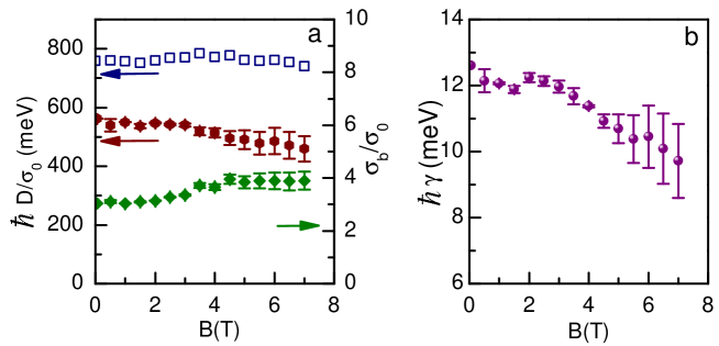
Figure 3a shows the spectral weight of the plasmon resonance peak and the background conductivity as a function of magnetic field, obtained by fitting and to the effective medium model, as described in the main text. Although the parameter shows a small decrease with magnetic field, there is no reason to associate this with a true decrease of the intraband spectral weight. In fact, the spectral weight defined as the integrated experimental optical conductivity (from 2 to 85 meV), , shown in Figure 3a as open square symbols, is roughly constant. This is related to the fact that the background conductivity shows a slight increase with field, which effectively compensates the decrease of . One can speculate about the possible origin of the background term. It may be partially due to an experimental uncertainty in the transmission normalization procedure. It is not excluded, however, that mimics a transfer of spectral weight from the main peak to higher energies, due to electron-electron PeresPRB06S , electron-phonon interactions ParkNanoLett08S ; CarbottePRB10S or excitations of higher harmonic plasmon resonancesLeavittPRB86S ; MikhailovPRB96S ; NikitinArxiv11S . An interesting possibility is that the negative charge removed from graphene forms a weakly conductive layer in SiC, which causes a highly overdamped Drude peak seen as a background in the studied spectral range. Notably, a certain optical background below the onset of interband absorption was present in exfoliated monolayer graphene on Si/SiO2LiNaturePhys08S .
We also observe a decrease of the plasmon scattering rate, as shown in Figure 3b. A plausible explanation is that the apparent scattering rate is determined not only by the intrinsic electronic scattering, but also by a statistical distribution of the resonance energy due to a varying size of homogeneous regions and anisotropy. At high fields the position of the peak is less influenced by the plasmon energy and the effect of statistical distribution is weaker.
References
- (1) Allen, S. J.; Stormer, H. L.; Hwang, J. C. M. Phys. Rev. B 1983, 28, 4875-4877.
- (2) Leavitt R. P.; Little, J. W. Phys. Rev. B 1986, 34, 2450-2457.
- (3) Mikhailov, S. A. Phys. Rev. B 1996, 54, 10335-10338.
- (4) Peres, N. M. R.; Guinea, F.; Castro Neto, A. H. Phys. Rev. B 2006, 73, 125411.
- (5) Park, C. H.; Giustino, F; Cohen,; Louie, S. G. Nano Lett. 2008, 8, 4229.
- (6) Carbotte, J. P.; Nicol, E. J.; Sharapov, S. G. Phys. Rev. B 2010, 81, 045419.
- (7) Nikitin, A. Y.; Guinea, F.; Garcia-Vidal, F. J.; Martin-Moreno, L. Phys Rev B 2012, 85, 081405.
- (8) Li, Z. Q.; Henriksen, E. A.; Jiang, Z.; Hao, Z.; Martin, M. C.; Kim, P.; Stormer, H. L.; Basov, D. N. Nat. Phys. 2008, 4, 532-535.