Observation of the fractional a.c. Josephson effect and the signature of Majorana particles
Abstract
Topological superconductors which support Majorana fermions are thought to be realized in one-dimensional semiconducting wires coupled to a superconductor Lutchyn2010a ; Oreg2010 ; Alicea2011 . Such excitations are expected to exhibit non-Abelian statistics and can be used to realize quantum gates that are topologically protected from local sources of decoherence Kitaev2001 ; Kitaev2003 . Here we report the observation of the fractional a.c. Josephson effect in a hybrid semiconductor/superconductor InSb/Nb nanowire junction, a hallmark of topological matter. When the junction is irradiated with a radio-frequency in the absence of an external magnetic field, quantized voltage steps (Shapiro steps) with a height are observed, as is expected for conventional superconductor junctions, where the supercurrent is carried by charge- Cooper pairs. At high magnetic fields the height of the first Shapiro step is doubled to , suggesting that the supercurrent is carried by charge- quasiparticles. This is a unique signature of Majorana fermions, elusive particles predicted ca. 80 years ago Majorana37 .
In 1928 Dirac reconciled quantum mechanics and special relativity in a set of coupled equations, which became the cornerstone of quantum mechanicsDirac1928 . Its main prediction that every elementary particle has a complex conjugate counterpart – an antiparticle – has been confirmed by numerous experiments. A decade later Majorana showed that Dirac’s equation for spin-1/2 particles can be modified to permit real wavefunctionsMajorana37 ; Wilczek2009 . The complex conjugate of a real number is the number itself, which means that such particles are their own antiparticles. While the search for Majorana fermions among elementary particles is ongoing Cho2011 , excitations with similar properties may emerge in electronic systemsKitaev2001 , and are predicted to be present in some unconventional states of matter moore91 ; Sengupta2001 ; DasSarma2006 ; Read2000 ; fu08 ; sau10 .
Ordinary spin-1/2 particles or excitations carry a charge, and thus cannot be their own antiparticles. In a superconductor, however, free charges are screened, and charge-less spin-1/2 excitations become possible. The BCS theory allows fermionic excitations which are a mixture of electron and hole creation operators, . This creation operator is invariant with respect to charge conjugation, . If the energy of an excitation created in this way is zero, the excitation will be a Majorana particle. However, such zero-energy modes are not permitted in ordinary -wave superconductors.
The current work is inspired by the paper of Sau et al. sau10 who predicted that Majorana fermions can be formed in a coupled semiconductor/superconductor system. Superconductivity can be induced in a semiconductor material by the proximity effect. At zero magnetic field electronic states are doubly-degenerate and Majorana modes are not supported. In semiconductors with strong spin-orbit (SO) interactions the two spin branches are separated in momentum space, but SO interactions do not lift the Kramer’s degeneracy. However, in a magnetic field there is a range of energies where double degeneracy is liftedQuay2010 , see schematic in Fig 1c. If the Fermi energy is tuned to be within this single-mode range of energies, , (where is the proximity gap, is the Zeeman energy, is the Bohr magneton, and is the Landé -factor), the proximity effect from a conventional -wave superconductor induces -wave pairing in the semiconductor material and drives the system into a topological superconducting state which supports Majorana particles. Theoretically, it has been predicted that proper conditions for this to occur can be realized in 2D sau10 ; Alicea2010 and, most relevant to the current work, in 1D systemsLutchyn2010a ; Oreg2010 . Moreover, multiband nanowires should also support topological superconductivityLutchyn2010 ; Potter2010 ; Stanescu2011 .
What are the experimental signatures of Majorana particles? Majorana particles come in pairs, and zero energy Andreev end-modes localized at the ends of a wire can be probed in tunneling experimentsSengupta2001 ; Law2009 ; sau2010a . Indeed, there are reports of zero bias anomaly observed in topological insulator/superconductorKoren2011 and semiconductor/superconductorMourik2012 ; Deng2012 structures. However, conductivity enhancement near zero bias can also be a signature of diverse phenomena in mesoscopic physics, such as the Kondo effect in quantum dotsgoldhaber98a ; rokhinson99a or the “0.7 anomaly” in nanowirescronenwett02 ; rokhinson06 . Fusion of two Majorana modes produces an ordinary fermion and, uniquely to Majorana particles, modifies periodicity of the Josephson relation from (Cooper pairs) to (Majorana particles)Kitaev2001 ; Kwon2004 ; Fu2009 ; Lutchyn2010a ; Akhmerov2011 . In the dc Josephson effect, fluctuations between filled and empty Majorana modes will mask the periodicity and, indeed, we observe only periodicity in a dc SQUID configuration. In the ac Josephson effect, however, the periodicity due to Majorana modes should be fully revealed.
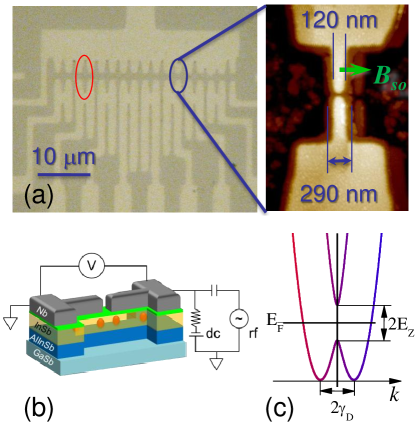
In our experiments Nb/InSb/Nb Josephson junctions (JJs) are fabricated lithographically from a shallow InSb quantum well. Superconductivity in InSb is induced by the proximity effect from a Nb film placed on top of the InSb nanowire. The self-aligning fabrication process which we use is described in the Supplementary Information. A pattern of multiple JJs is defined by e-beam lithography, and a 45 nm layer of Nb is deposited by dc sputtering on top of the InSb quantum well. An image of a JJ region is shown in Fig. 1a. A weak link is formed between two 120 nm-wide and 0.6 m-long Nb wires, with gaps ranging from 20 to 120 nm in different devices. During deposition of Nb, a thin (2-4 nm) layer of Nb is extended 70-80 nm outside the pattern, including the space inside the gaps (a brown halo around the Nb wire on the AFM image). This layer is used as an etch mask to define a nanowire in the underlying semiconductor self-aligned to the Nb wire. After the etching a continuous nm-wide InSb wire is formed under the Nb, as shown schematically in Fig. 1b. The thin Nb layer is not conducting at low temperatures, so that the supercurrent is carried by the proximity-induced superconductivity in InSb.
The InSb wires have rectangular cross section and SO interactions are dominated by the Dresselhaus term , where , nm is the quantum well thickness, eVÅ3 for InSb, are Pauli matrices, and and are the principal crystallographic axes. We estimate meVsup . The wires are oriented along the [110] crystallographic direction, and expected direction of the effective spin-orbit magnetic field is perpendicular to the current, as indicated by the green arrow on the AFM image. At high fields () Majorana particles are expected to form inside the InSb wire close to the ends of the Nb wires. At these fields the supercurrent is dominated by the fusion of two Majorana particles across the gap, which amounts to the charge transfer. From the lithographical dimensions we estimate that only a few (1-3) one-dimensional subbands should be populated in InSb nanowires, however, we expect the density of states in the nanowires to be modified by the strong coupling to Nb and the actual number of filled subbands may be larger.
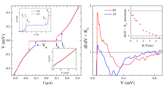
As devices are cooled down, a series of superconducting transitions and are observed (Fig. 2). The first transition, K, is for wide areas, K and K are for the 1 and 0.12 m-wide Nb wires, and is for the JJs. From K for JJ8 we estimate a proximity gap eV and a semiconductor-superconducting coupling Sau2012 . Lithographically our devices consist of two JJs in parallel, and we can measure the ratio of the critical currents in the two arms by measuring current modulation in a dc SQUID configuration. The ratio for JJ7 and for JJ8, indicating that conduction is dominated by a single junction. In the following analysis we will treat our devices as containing a single JJ.
As seen in Fig. 2, characteristic for JJ8 measured at the base temperature of 20 mK exhibits a clear supercurrent region (), with an abrupt appearance of a finite voltage. A small hysteresis is observed for the return critical current , characteristic of a resistively shunted JJ in an intermediate damping regimeTinkham-book96 . Indeed, we measure high leakage to the substrate, and estimate the shunting resistance k. The measured resistance in the normal state is , and the actual normal resistance of the JJ8 k, consistent with the number of 1D channels estimated from the size of the wire. The product mV indicates that JJ8 is in a clean limit (weak link length , where is the coherence length and is the mean free path), a proper condition for the formation of Majorana particles.
Normalized differential conductance, plotted in the right panel of Fig. 2, shows enhancement at low voltages. This excess current is a signature of Andreev reflectionAndreev1964 ; Doh2005 . Most important for our measurements is that the excess current, and thus coherent electron transport, is observed at high in-plane magnetic fields up to 4 T, as shown in the the inset.
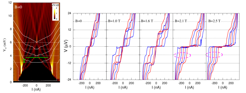
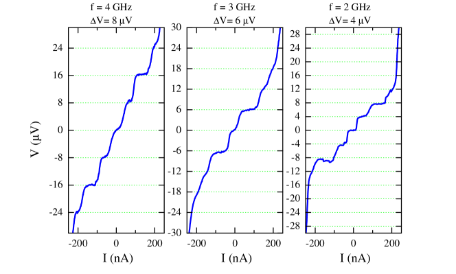
In the presence of a microwave excitation, phase locking between the rf field and the Josephson supercurrent gives rise to constant-voltage Shapiro steps in the characteristics at , where is Planck’s constant, is the charge of quasiparticles, is the microwave frequency, and Shapiro1963 . Shapiro steps for GHz are shown in Fig. 3. At we observe steps with the height V, consistent with the Cooper pair tunneling (). scales linearly with sup . The evolution of the steps with is best visualized in the plots, where steps with are seen at high rf powers. A transition from low to high rf power regime is clearly seen in the plot near mV and is marked by a green horizontal line. At high rf powers mV the evolution of the width of the Shapiro steps follows a Bessel function pattern as a function of power, , where is the rf amplitude at the junction. We can find the rf power attenuation from the fit to the , for GHz, Fig. 4. Here is the rf amplitude at the top of the fridge. Thus, mV corresponds to V, where V, see Fig. 2.
For mV the junction is in the small microwave signal regime LikharevJJbook . The linear response of a JJ has a singularity at , where is the Josephson frequency, and the JJ performs a parametric conversion of the external frequency. The JJ8 is in the intermediate damping regime and the characteristic is expected to become non-hysteretic in the vicinity of the first step. Indeed, we observe no hysteresis for mV. While nonlinear effects can be present at high and , we want to stress that the first step at the onset of the normal state is due to phase locking between the external and the Josephson frequencies, .
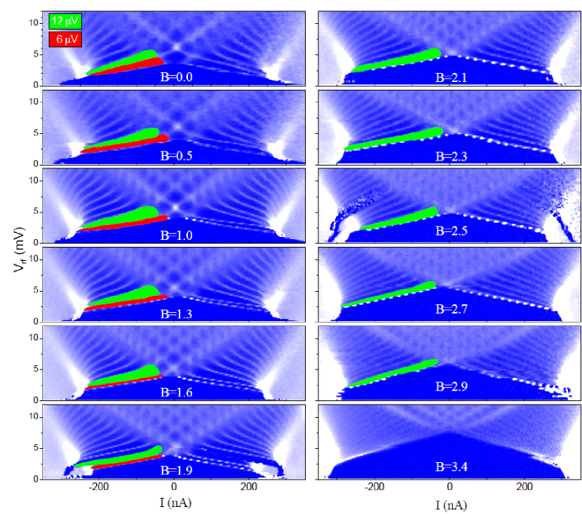
When in-plane magnetic field is applied, Shapiro steps at and 18 V are clearly visible at low fields, T. Steps at 12 and 18 V remain visible up to T, while the step at 6 V disappears above T. The disappearance of all steps above 3 T is consistent with suppression of the excess current and Andreev reflection at high fields.
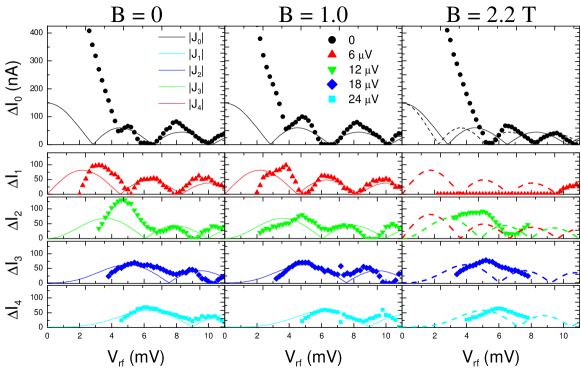
Quantitative comparison of the width of the Shapiro steps for different extracted from data is plotted in Fig. 4. For T steps at 0, 6, 12, 18 and 24 V evolve according to Bessel functions with the amplitude nA. For T the step at 6 V vanishes at low , and re-appears at high mV for T. We also observe that the low field rf attenuation does not fit the evolution of the plateau. Moreover, a minimum of the 12 V plateau at meV coincides with the minimum of the Bessel function, suggesting that indeed the 12 V plateau became the Shapiro step. Evolution of plateaus at T is poorly described by Bessel functions, suggesting that oscillations with different frequencies may contribute to the width if the plateaus. We emphasize that the doubling of the Shapiro step height is a unique signature of a topological quantum phase transition.
Theoretically it has been argued that Josephson current with both () and () periodicity should be present in the topological stateAlicea2011 ; Jiang2011 ; Pikulin2011 ; San-Jose2011a , especially in a multichannel wires. However, in current–biased junctions odd steps are expected to vanish even in the presence of large supercurrents carried by the charge- quasiparticles Dominguez2012 . In this case the width of even steps is expected to be defined primarily by and the coefficient remains almost unchanged across the transition, as is observed experimentally, especially if a large number of subbands is occupied in the nanowire due to the strong coupling to the superconductor. At high voltages across the junction we expect enhanced mixing between gapless and gapped modes, which may explain the prominence of the 18 V and higher plateaus at T.
Acknowledgements The work was partially supported by ARO grant W911NF-09-1-0498 (L.P.R.) and by NSF grant DMR10-05851 (J.K.F., X.L.). L.P.R. benefited from discussions with Roman Lutchyn.
Authors contributions L.P.R. conceived and performed the experiments; J.K.F. and X.L. designed and grew the heterostructures; all authors contributed to the writing of the manuscript.
Supplementary Information
Observation of fractional ac Josephson effect: the signature of Majorana particles
Leonid P. Rokhinson, Xinyu Liu and Jacek K. Furdyna
I Analysis of the parameter space to observe fractional Josephson effect
In order to form Majorana fermions in a nanowire, several conditions have to be satisfied. The most stringent is lifting of the Kramers degeneracy, , where is Zeeman energy , for InSb, is Bohr magnetron, and is an external magnetic field. At the same time we need the proximity gap to be larger than the Josephson frequency, eV for 3 GHz, or in the topological phase. The proximity gap depends on the semiconductor-superconductor coupling , Zeeman energy and spin-orbit coupling Sau2012 :
| (S1) |
The maximum cannot exceed the superconducting gap in narrow Nb wires, eV for K, and is maximized for large coupling . Large coupling, though, increases electron density in the semiconductor which, in turn, increases , thus requiring large fields to lift the Kramers degeneracy.
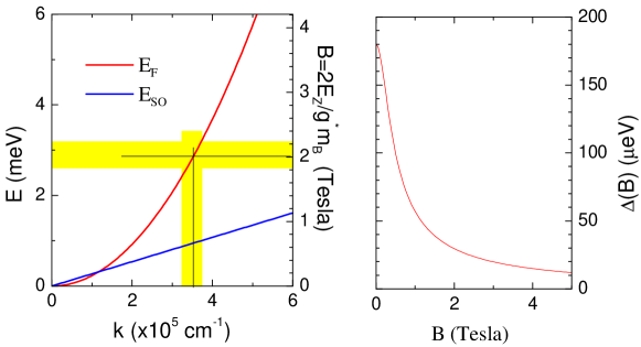
Let us analyze the parameters of the JJ8 device. We measured K, thus eV and eV, or . In our sample geometry we cannot measure electron density independently, but we can assume that at Tesla (observed topological phase transition) . We plot , and as a function of in Fig. S5. Here we use eVÅ3, , effective mass , effective -factor , and the quantum well thickness nm. At T ( meV) the condition translates into cm-1. Spin-orbit coupling for this is estimated meV. The expected field dependence of the proximity gap is plotted on the right plot for meV. We see that at T eV and the condition is satisfied.
We observe Shapiro steps up to T, which is consistent with the theoretically expected gap to be only eV at that field. Experimentally we measure a weaker vs dependence than the one predicted by Eq. (S1), see Section IV.
The maximum width of the InSb wire is 290 nm, and we expect the actual InSb wire width to be reduced due to side etching and surface depletion. For an InSb wire with width nm the energy separation between the first 2 energy levels is 1.2-8 meV and only subbands are expected to be occupied for meV. We note, though, that strong coupling to Nb modifies the density of states in the InSb wire and the actual number of filled subbands may be larger. Thus, we conclude that experimental parameters for the JJ8 device satisfy the requirements for the observation of Majorana fermions.
II Fabrication of Josephson junctions

The starting material is undoped In0.6Ga0.4Sb/InSb/In0.6Ga0.4Sb (3nm/20nm/3nm) quantum well grown by molecular beam epitaxy on a Te-doped (001) GaSb substrate. A thick graded InxGa1-xSb () buffer and a 120nm In0.77Al0.33Sb barrier were grown between the wafer and the quantum well for strain relaxation and electron confinement. A pattern of multiple JJs is defined by e-beam lithography, and a 45 nm thick layer of Nb is deposited by dc sputtering. Surface oxide is removed by dipping the sample in HF:DI (1:10) for 20 seconds prior to Nb deposition. An optical image of a multi-device sample is shown in Fig. S6. Weak links are formed between two 120 nm-wide and 0.6 m-long Nb wires, with gaps in 20-120 nm range.
The key processing step is self alignment of the Nb and InSb wires. We use double layer MMA/PMMA photoresist which creates an undercut after e-beam exposure and development. During Nb sputtering at mTorr of Argon some Nb is scattered into this undercut area and a thin (2-4 nm) layer of Nb is formed, extending 70-80 nm outside the pattern, including the space inside the gaps (a brown halo around the wire in the AFM image; see also Fig. S7). This layer is used as an etch mask to define a nanowire in the underlying semiconductor, which becomes self-aligned to the Nb wire. Etching in H2SO4:H2O2:H2O (1:8:1000) for 30 sec removes 60 nm of semiconductor and a continuous nm-wide InSb wire is formed under the Nb (we expect that the width of the wire is reduced during the wet etching step by nm from each side).
III Proximity effect
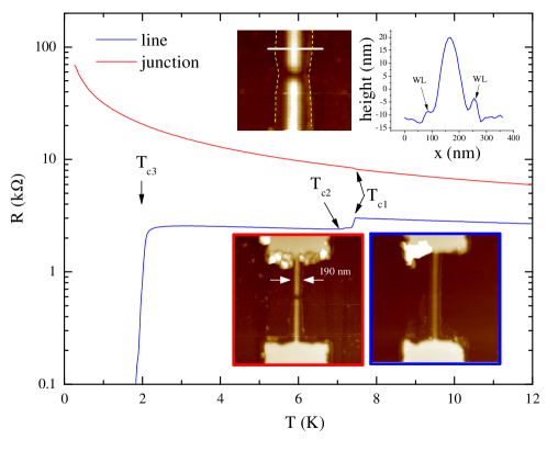
In order to verify that we observe proximity-induced superconductivity, we fabricated several () test devices on a semi-insulating GaAs substrate with the Nb pattern identical to the JJ devices, see inset in Fig. S7. Continuous wires show the expected superconducting phase transitions at K for wide regions (m), K for 1 m wide connectors and K for the 80 nm-wide wire. There is a 4 nm thick wetting layer around Nb, which can be seen as a halo around wires on the micrographs. For wires with small gaps nm the wetting layer fills the gap. The wetting layer is not attacked by the etching solution and serves as an etch mask in the semiconductor wire definition. In the device shown in Fig. S7 the gap is nm. Yet these devices become insulating when cooled to low temperatures. This test experiment allows us to establish that (i) the thin Nb layer is not conducting and plays no role in the electrical transport, (ii) the tunneling current for gaps nm is negligible, and (iii) in InSb JJs the current has to flow through the InSb layer. Thus the observed superconductivity in InSb JJs is due to the proximity effect.
IV Temperature dependence of JJ
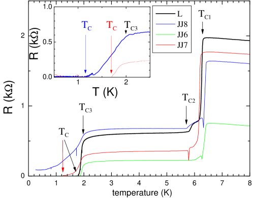
Proximity-induced superconductivity has a reduced gap compared to the gap of the host superconductor, Eq. (S1). The lowest corresponds to this reduced proximity gap.
Temperature dependence of samples resistance is shown in Fig. S8. For a continuous line (L) we can identify three transition temperatures: K is for wide regions, K is for 1 m-wide wires and K is for the 150 nm-wide wire. Similar results are obtained for Nb on GaAs, Section III. Devices with a Josephson junctions (JJ6-8) have the actual superconducting transition for various devices. Note that in a 3He refrigerator, where electrical noise is higher, we do not observe the superconducting transition for the JJ8 device down to 250 mK, the actual for this device is 1.17 K, see inset.
V Magnetic field dependence of critical current
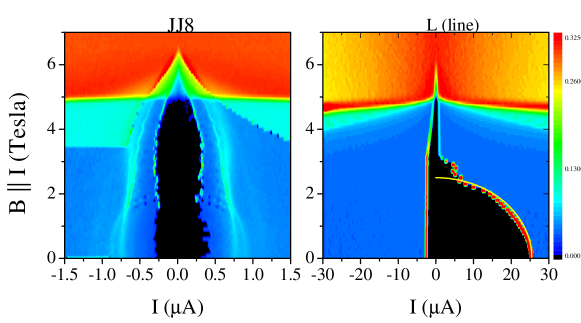
The requirement is that the proximity gap in the semiconductor material at the magnetic fields needed to satisfy the condition . In our Nb wires superconductivity survives up to 5 Tesla, see Fig. S9. In the low field region with T. Resistivity of crystalline Nb is 152 nm and a perfect m, nm and nm wire should have resistance of . Our wires have resistance of k, which indicates a substantial degree of disorder. Neither nor are expected to be substantially affected by the disorder Tinkham-book96 , consistent with the measured K compared to the K in pure crystalline Nb. Disordered Nb is a type-II superconductor, and superconducting gap survives to much higher field T. The thickness of the film nm is of the order of the coherence length in Nb (39 nm), thus flux capturing is possible even for the in-plane field.
VI Frequency dependence of Shapiro steps
In Fig. S10 we show traces measured in the presence of rf field with frequencies , 3 and 4 GHz. The corresponding step heights are, respectively, , 6 and 8 V.
VII Analysis of the Josephson junction
The wafers used in these experiments have substantial leakage between the Nb film and a heavily doped substrate, and the substrate forms a shunting resistance to every device. We can estimate the shunting resistance and the normal resistance of the JJ8 as follows. Next to the JJ we fabricate a 0.12 m-wide wire with a measured resistance in the normal state of k. An identical wire on an insulating GaAs substrate has a resistance of k, thus the shunting resistance for the wire device k. The wire device and the JJ devices have similar layouts and we assume that the shunting resistances are similar, (the leakage to the substrate is primarily through contact pads of the same size). The measured resistance of the JJ8 in the normal state is k, thus we estimate k. The JJ8 device consists of two nominally identical JJs in parallel, and the actual for the dominant junction can be as high as k. Thus, JJ8 has a few () subbands, which is also consistent with the number of subbands estimated from the size quantization, see Section I.
For short weak links in the dirty regime ( and , where is the mean free path, is the coherence length, and is the effective length of the weak link), the product Likharev1979 . For the clean regime () the value should be almost twice as large, . From the above estimates the product mV, while K. Thus, JJ8 is in the clean regime, which is favorable for the observation of Majorana fermions.
VIII Analysis of Shapiro steps as a function of rf power
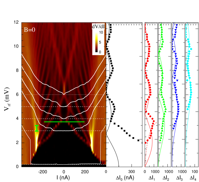
In Fig. S11 we plot differential resistance at for the JJ8 device. Shapiro steps with V are clearly seen at mV and correspond to the black regions on the contour plot. At high mV evolution of the width of the Shapiro steps follows the Bessel function pattern as a function of power, , where is the rf amplitude at the junction and is the rf frequency. We can estimate the rf power attenuation from the fitting of with above mV, at GHz and at GHz. Here is the rf amplitude at the top of the fridge.
In the plot we can identify two regions with different dependencies, separated schematically by a green line at mV. For the JJ8 device , see Fig. 2 of the manuscript, and for the junction is in the small microwave signal regime LikharevJJbook . The linear response of a JJ has a singularity at , and the first Shapiro step appears due to phase locking of the external frequency and the Josephson oscillations. The JJ8 is in the intermediate damping (resistively shunted) regime, and the characteristic is expected to become non-hysteretic in the vicinity of the first step. Indeed, we observe no hysteresis for mV. While nonlinear effects can be present at high and we want to stress that the first step at the onset of the normal state is due to phase locking between the external and the Josephson frequencies, .
The width of the first step in the low rf power regime is expected to be ; see dashed red line on plot. At high power the width of the -th step is expected to follow the -th Bessel function. Indeed the step widths follow the expected pattern, but some deviations are expected due the sample being in a crossover regime between the low and the high rf power regimes.
IX Magnetic field dependence of the Shapiro steps
References
- (1) Lutchyn, R. M., Sau, J. D. & Sarma, S. D. Majorana fermions and a topological phase transition in semiconductor-superconductor heterostructures. Phys. Rev. Lett. 105, 077001 (2010).
- (2) Oreg, Y., Refael, G. & von Oppen, F. Helical liquids and Majorana bound states in quantum wires. Phys. Rev. Lett. 105, 177002 (2010).
- (3) Alicea, J., Oreg, Y., Refael, G., von Oppen, F. & Fisher, M. P. A. Non-Abelian statistics and topological quantum information processing in 1d wire networks. Nat Phys 7, 412–417 (2011).
- (4) Kitaev, A. Y. Unpaired Majorana fermions in quantum wires. Physics-Uspekhi 44, 131 – 136 (2001).
- (5) Kitaev, A. Y. Fault-tolerant quantum computation by anyons. Ann. Phys. 303, 2–30 (2003).
- (6) Majorana, E. Symmetrical theory of electrons and positrons. Nuovo Cimento 14, 171 – 184 (1937).
- (7) Dirac, P. A. M. The quantum theory of the electron. Proc. R. Soc. Lond. A 117, 610–624 (1928).
- (8) Wilczek, F. Majorana returns. Nat Phys 5, 614–618 (2009).
- (9) Cho, A. The sterile neutrino: Fertile concept or dead end? Science 334, 304–306 (2011).
- (10) Moore, G. & Read, N. Nonabelions in the fractional quantum Hall effect. Nuc. Phys. B 360, 362–396 (1991).
- (11) Sengupta, K., Žutić, I., Kwon, H.-J., Yakovenko, V. M. & Das Sarma, S. Midgap edge states and pairing symmetry of quasi-one-dimensional organic superconductors. Phys. Rev. B 63, 144531 (2001).
- (12) Das Sarma, S., Nayak, C. & Tewari, S. Proposal to stabilize and detect half-quantum vortices in strontium ruthenate thin films: Non-abelian braiding statistics of vortices in a superconductor. Phys. Rev. B 73, 220502 (2006).
- (13) Read, N. & Green, D. Paired states of fermions in two dimensions with breaking of parity and time-reversal symmetries and the fractional quantum Hall effect. Phys. Rev. B 61, 10267–10297 (2000).
- (14) Fu, L. & Kane, C. Superconducting proximity effect and Majorana fermions at the surface of a topological insulator. Physical Review Letters 100, 096407 (2008).
- (15) Sau, J., Lutchyn, R., Tewari, S. & Das Sarma, S. Generic new platform for topological quantum computation using semiconductor heterostructures. Physical Review Letters 104, 040502 (2010).
- (16) Quay, C. et al. Observation of a one-dimensional spin-orbit gap in a quantum wire. Nature Physics 6, 336 – 339 (2010).
- (17) Alicea, J. Majorana fermions in a tunable semiconductor device. Phys. Rev. B 81, 125318 (2010).
- (18) Lutchyn, R. M., Stanescu, T. & Sarma, S. D. Search for Majorana fermions in multiband semiconducting nanowires. Phys. Rev. Lett. 106, 127001 (2011).
- (19) Potter, A. C. & Lee, P. A. Multichannel generalization of Kitaev’s Majorana end states and a practical route to realize them in thin films. Phys. Rev. Lett. 105, 227003 (2010).
- (20) Stanescu, T., Lutchyn, R. M. & Sarma, S. D. Majorana fermions in semiconductor nanowires. Phys. Rev. B 84, 144522 (2011).
- (21) Law, K. T., Lee, P. A. & Ng, T. K. Majorana fermion induced resonant Andreev reflection. Phys. Rev. Lett. 103, 237001 (2009).
- (22) Sau, J. D., Tewari, S., Lutchyn, R., Stanescu, T. & Sarma, S. D. Non-abelian quantum order in spin-orbit-coupled semiconductors: The search for topological Majorana particles in solid state systems. Phys. Rev. B 82, 214509 (2010).
- (23) Koren, G., Kirzhner, T., Lahoud, E., Chashka, K. B. & Kanigel, A. Proximity-induced superconductivity in topological Bi2Te2Se and Bi2Se3 films: Robust zero-energy bound state possibly due to Majorana fermions. Phys. Rev. B 84, 224521 (2011).
- (24) Mourik, V. et al. Signatures of Majorana fermions in hybrid superconductor-semiconductor nanowire devices. Science 336, 1003 – 1007 (2012).
- (25) Deng, M. T. et al. Observation of Majorana fermions in a Nb-InSb nanowire-Nb hybrid quantum device (2012). eprint arXiv:1204.4130.
- (26) Goldhaber-Gordon, D. et al. Kondo effect in a single-electron transistor. Nature 391, 156 – 159 (1998).
- (27) Rokhinson, L. P., Guo, L. J., Chou, S. Y. & Tsui, D. C. Kondo-like zero-bias anomaly in electronic transport through an ultrasmall Si quantum dot. Phys. Rev. B 60, R16319 – 21 (1999).
- (28) Cronenwett, S. M. et al. Low-temperature fate of the 0.7 structure in a point contact: a Kondo-like correlated state in an open system. Phys. Rev. Lett. 88, 226805 (2002).
- (29) Rokhinson, L., Pfeiffer, L. & West, K. Spontaneous spin polarization in quantum point contacts. Phys. Rev. Lett. 96, 156602 (2006).
- (30) Kwon, H.-J., Sengupta, K. & Yakovenko, V. Fractional ac Josephson effect in p- and d-wave superconductors. The European Physical Journal B 37, 349–361 (2003).
- (31) Fu, L. & Kane, C. L. Josephson current and noise at a superconductor/quantum-spin-Hall-insulator/superconductor junction. Phys. Rev. B 79, 161408 (2009).
- (32) Akhmerov, A. R., Dahlhaus, J. P., Hassler, F., Wimmer, M. & Beenakker, C. W. J. Quantized conductance at the Majorana phase transition in a disordered superconducting wire. Phys. Rev. Lett. 106, 057001 (2011).
- (33) Refer to the Supplementary Informartion.
- (34) Sau, J. D., Tewari, S. & Das Sarma, S. Experimental and materials considerations for the topological superconducting state in electron and hole doped semiconductors: searching for non-Abelian Majorana modes in 1d nanowires and 2d heterostructures. Phys. Rev. B 85, 064512 (2012).
- (35) Tinkham, M. Introduction to superconductivity (McGraw-Hill, New York, 1996).
- (36) Andreev, A. Thermal conductivity of the intermediate state of superconductors. Zhurnal Eksperimental’noi i Teoreticheskoi Fiziki 46, 1823 – 1828 (1964).
- (37) Doh, Y.-J. et al. Tunable supercurrent through semiconductor nanowires. Science 309, 272–275 (2005).
- (38) Shapiro, S. Josephson currents in superconducting tunneling: The effect of microwaves and other observations. Phys. Rev. Lett. 11, 80–82 (1963).
- (39) Likharev, K. K. Dynamics of Josephson junctions and circuits (Gordon and Breach Science Publishing, Paris, 1984).
- (40) Jiang, L. et al. Unconventional Josephson signatures of Majorana bound states. Phys. Rev. Lett. 107, 236401 (2011).
- (41) Pikulin, D. I. & Nazarov, Y. V. Phenomenology and dynamics of Majorana Josephson junction (2011). eprint arXiv:1112.6368.
- (42) San-Jose, P., Prada, E. & Aguado, R. AC Josephson effect in finite-length nanowire junctions with Majorana modes. Phys. Rev. Lett. 108, 257001 (2011).
- (43) Domínguez, F., Hassler, F. & Platero, G. On the dynamical detection of Majorana fermions in current-biased nanowires (2012). eprint arXiv:1202.0642.
- (44) Likharev, K. K. Superconducting weak links. Rev. Mod. Phys. 51, 101–159 (1979).