Graphene-based polaritonic crystal
Abstract
It is shown that monolayer graphene deposited on a spatially-periodic gate behaves as a polaritonic crystal. Its band structure depending on the applied gate voltage is studied. The scattering of electromagnetic radiation from such a crystal is presented calculated and analyzed in terms of Fano-type resonances between the reflected continuum and plasmon-polariton modes forming narrow bands.
pacs:
81.05.ue,72.80.Vp,78.67.WjCoupling of light to the surface charges at a metal-dielectric interface gives rise to a special kind of evanescent electromagnetic (EM) waves called surface plasmon-polaritons (SPPs) c:SPP-common . The specific properties of SPPs allow for their use in variety of practical applications. The sensitivity of SPPs to the properties of the dielectric, the metal and the interface is used in SPP-based sensors c:sensors ; Shalabney2011 and in high-resolution imaging Barnes2003 ; c:zayats ; c:imaging . Surface plasmons give rise to very large EM fields at the surface, which is important for surface-enhanced optical spectroscopies Hartland2011 . Moreover, the SPP wavelength can be much smaller than the photon wavelength, opening the possibility for further miniaturization of photonics components, a new field of research called nanoplasmonics c:plasmonics . Of particular interest is the ability to tune SPP modes in plasmonic devices by external control: using an electric field in a liquid crystal c:liq-crys , a magnetic field in a magneto-optically active substrate c:mag-f , thermal heating c:heating , or a light beam focused on a non-linear coating c:nonlinear .
The possibility of tuning the amount of free carriers in graphene using an external gate allows for an effective control of the material’s optical properties c:graphene-review ; c:graphene-gating ; c:graphene-optics ; Koppens2011 . Exploring graphene, a tunable two-dimensional (2D) metal, for plasmonics at the nano-scale reveals new physical effects and opens exciting possibilities in this field c:graphene-plasmons ; c:graphene-plasmons-TE ; c:disp-rel ; c:graphene-plas-tuning . When compared to their counterparts in conventional 2D electron systems, SPPs in graphene exhibit some new and unusual properties, such as the -power density dependence of the SPP frequency c:graphene-plasmons and the existence of -polarized waves c:graphene-plasmons-TE . Moreover, SPPs in graphene can potentially be used in a variety of practical applications. For example, using the amplification of SPPs in graphene opens the possibility to create a terahertz radiation source c:graphene-plas-source ; employing the attenuated total reflection (ATR) configuration with a gated graphene layer allows for a resonant switching of the reflection coefficient of an external EM wave from nearly unity to almost zero c:switch .


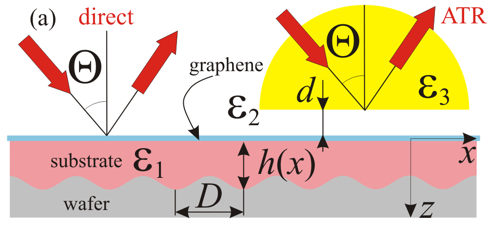
Recently, a new class of metamaterials based on SPPs in graphene, either deposited on a periodically corrugated surface c:waveguide or composed of an array of micro-ribbons Ju2011 was proposed, with a high potential interest for transformation optics. When SPPs propagate along a periodically modulated surface, the concept of a ”surface polaritonic crystal” can be introduced c:zayats , where the SPP dispersion shows a band-gap structure c:band-gap-spp , in analogy with a photonic crystal. In this Letter we propose and theoretically analyze a new type of SPP crystal, based on a graphene sheet deposited on top of a periodically modulated gate electrode (wafer), as schematically represented in Fig. 1(a).
In order to achieve the periodic modulation of graphene’s conductivity, we consider a single graphene layer in the plane deposited on a SiO2 substrate with a dielectric constant [see Fig. 1(a)]. The opposite side of the substrate has a periodic relief with a spatial period , such that . To be specific, we will consider the dielectric thickness modulation of the form , where is the modulation depth and . A conductive wafer is placed over this modulated surface, serving as a gate contact. If a constant gate voltage is applied between the graphene layer and the wafer, a periodic modulation of the garphene conductivity can be achieved. If , the carrier density in graphene can be expressed as , where is the electron charge and is a coefficient between 1 and 2 depending on the charge distribution on the corrugated gate electrode (further in the Letter we use ). Owing to the periodicity of the surface relief, the carrier density in graphene is a periodic function with the same period , thus resulting in the periodicity of its optical conductivity, . The latter can be related to the local value of the chemical potential counted with respect to the Dirac point, , where is the Fermi velocity.
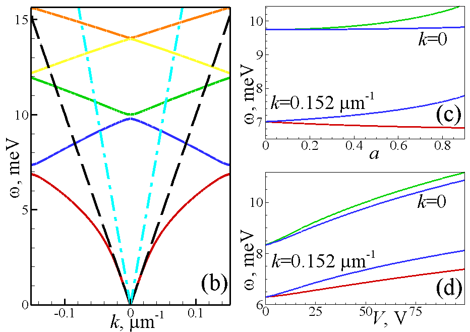
As it is shown below, the periodic modulation of the optical conductivity leads to the possibility of direct coupling of a propagating EM wave to the surface plasmons (Fig. 1(a), left, where is the dielectric constant of the medium above graphene). However, only those SPP modes which lie within the light cone, , shown by dash-dotted lines in Fig. 1(b), can be excited this way. In general, for the SPP excitation one has to consider an ATR structure like the one described in Ref. c:switch, , which includes a prism with a dielectric constant (Fig. 1(a), right). Usually there is a gap between the graphene sheet and the prism, which we shall model as a dielectric layer of a thickness and a dielectric constant . We assume that the prism occupies the half-space and a -polarized EM wave impinges on the boundary , coming from at an angle of incidence .
Since the dielectric properties of the structure are periodic along , the solution of Maxwell’s equations, , for the -polarized wave [with components and ] can be written as Fourier-Floquet series:
In Eqs. (Graphene-based polaritonic crystal) and (Graphene-based polaritonic crystal), is the in-plane component of the photon wavevector in the medium (; applies only for the ATR configuration), , and is the speed of light in vacuum. Although the substrate is finite, for simplicity we shall consider the medium 1 as semi-infinite in the wave equations. If the gate electrode is transparent, this simplification is not crucial for the analysis of the optical properties of the modulated structure. Boundary conditions at imply the continuity of the tangential components of the electric and magnetic fields, [, ]. At , the tangential component of the electric field is continuous, , while the discontinuity of the tangential component of the magnetic field, , stems from the presence of surface currents (caused by the SPP electric field) in the graphene layer. Applying these boundary conditions, one can find the explicit form of the transfer matrices, , which relate the coefficients in Eqs. (Graphene-based polaritonic crystal) and (Graphene-based polaritonic crystal) for different , . The matrices consist of 22 blocks ,
| (5) | |||
| (8) |
where , , is a Kronecker symbol, is the spatial Fourier transform of the graphene conductivity.

The meaning of the coefficients , is different for the different media. The waves corresponding to the different terms in Eqs. (Graphene-based polaritonic crystal) and (Graphene-based polaritonic crystal) can be either propagating (with ) or evanescent (with ). Since the incident wave in the medium 3 possesses only the component (zero harmonic), and the coefficients are proportional to the magnetic field amplitude () in the incident wave. In the medium 1, the coefficients correspond to the absence of the corresponding harmonics coming from . Then, multiplying the matrices , and taking into account the block-diagonal structure of the matrix , after some algebra we obtain the following equations for the amplitudes of the reflected harmonics, :
| (9) |
where the elements of the matrix and the vector are
| (10) | |||
| (11) |
with and .
In order to obtain the general properties of SPPs in graphene with periodically modulated conductivity, we first consider the eigenvalue problem for the matrix leading to the dispersion relation for SPPs in a flat 2D graphene layer placed between two lossless dielectric media ( and ). We put and solve the equation . It yields complex eigenvalues because the graphene conductivity has both real and imaginary parts, therefore the SPP eigenmodes are dissipative. The SPP dispersion curve for the real part of the frequency eigenvalue, , vs wavenumber for the first Brillouin zone, , is presented in Fig. 1(b). The imaginary part of the frequency (mode damping) is an order of magnitude smaller than . As it can be seen from Fig. 1(b), the SPP dispersion curve is periodic in the -space, with the period . There are bands of allowed SPP frequencies, separated by gaps opening at the edges and in the center of the Brillouin zone, where SPPs do not exist. As expected, the widths of the gaps increase with the increase of the modulation depth [Fig.1(c)]. A natural question arises: is it possible to control dynamically the gap widths through some nondestructive external knob? The positive answer to this question is evident from Fig. 1(d). Since the chemical potential of graphene can be tuned by the gate voltage, one can shift the spectral position and width of the gaps by changing . Therefore, the SPP crystal band structure can be controlled dynamically.
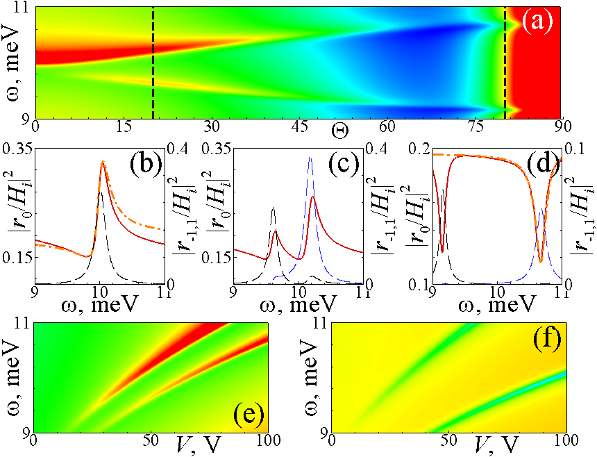
Another feature of the SPP spectrum in periodically modulated graphene is that the ”scan line”, located within the dash-dotted lines in Fig. 1(b) crosses the SPP dispersion curves. This situation is completely different from the case of uniform graphene c:switch , where both phase and group velocities of SPPs are smaller than the velocities of light in the surrounding dielectrics. SPPs in periodically modulated graphene can be excited by an external propagating EM wave, without an ATR prism. This is illustrated by Fig. 2, where the amplitudes of the reflected field harmonics are presented; they have been calculated by solving Eq. (9) for and (in this case, is real).
At normal incidence (), the zero harmonic reflection coefficient of the SPP crystal exhibits just one maximum at meV [see Figs. 2(a) and (b)], which approximately corresponds to the upper edge of the second gap in Fig. 1(b). This is related to the parity of the SPP mode with respect to , since it is excited by a plane wave and is an even function. Also from Fig. 2(b) it is clearly seen that the enhanced reflection of the zero harmonic corresponds to the excitation of the SPP harmonics with and . They correspond to the bottom of the third allowed SPP band and, for normal incidence, are mixed into the band bottom mode. For oblique incidence [Figs. 2(c)-(f)], there are two resonances corresponding to the second and third SPP bands and producing reflected field harmonics with . SPPs are effectively excited when the frequency and the in-plane component of the wave vector of the incident EM wave match those of SPP eigenmodes of the modulated graphene. The energy of the incident wave is transferred into the SPP harmonics with , while the refleted wave in the far field contains only zero harmonic. Note that the position and the amplitude of the resonances can be controlled by changing the gate voltage [Figs. 2(e) and 2(f)]. Quite interestingly, the direct excitation of and higher SPP bands can produce propagating EM waves with , scattered at angles
Let us focus on the characteristic spectral dispersion of the zero harmonic reflection coefficient around each of the SPP resonance frequencies [Figs. 2(b) and (c)] where an intrinsic mode of the SPP crystal is excited. This is an asymmetric Fano-type resonance with a maximum accompanied by a neighboring minimum. a phenomenon first discovered in the ionization spectra Fano of He and now known in many different branches of physics including light scattering by photonic crystals Fano-PhC . If a discrete mode couples to a continuum of excitations, the Fano resonance arises from the constructive (destructive) interference of the localized and delocalized waves, taking place above (below) the discrete mode frequency . A simple analytic expression to describe such a lineshape was suggested by Fano Fano :
| (12) |
where is the mode damping and is an assymetry parameter related to the relative strengths of the transitions associated with the discrete and continuum modes. Fig. 2(b) shows a Fano-type fit, to the calculated reflectivity spectrum ( and are constants). The coupling between the continuum of propagating EM modes in the medium 2 and the SPP Bragg mode of the polaritonic crystal decreases with the increase of the incidence angle. When is close to the Brewster angle, , the resonant excitation of modes results in two narrow and almost symmetric minima in the spectrum [see Fig. 2(d) where the Fano fit corresponds to , compared to in Fig. 2(b)].

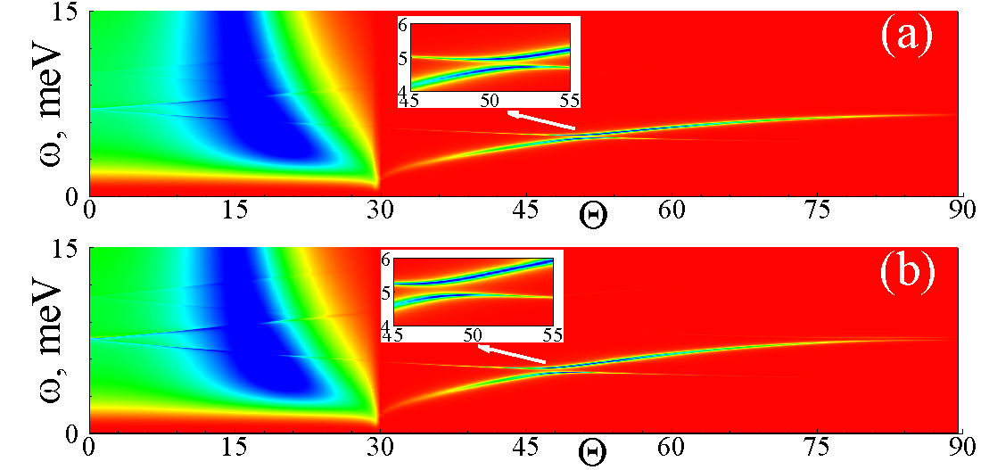
As mentioned above, the direct excitation of SPPs by a propagating wave allows for probing only the part of the polaritonic crystal band structure comprised between the dash-dotted light lines in Fig. 1(b). Beyond this, one has to use the ATR scheme where SPPs are excited by an evanescent wave with a sufficiently large wavenumber, The results calculated for the ATR structure are presented in Fig. 3, where the SPP excitation conditions correspond to a minimum of the zero harmonic reflectance related to the gap between the first and the second SPP bands. The mode anticrossing, corresponding to the edges of the gap, is clearly seen in Figs. 3(a) and 3(b) (near , see insets). Comparison of Figs. 3(a) and 3(b) shows, that increasing the gate voltage results in an increase of the gap width, as it could be anticipated from Fig. 1(f).
To conclude, we have demonstrated that a single graphene layer deposited on a ”sandwich”-like structure with a periodically corrugated gate electrode has the properties of a polaritonic crystal, namely, possesses a band structure with gaps that can be tuned by the gate voltage. This crystal exhibits Fano-type resonances in the reflectance of incident EM waves due to the excitation of plasmon-polariton Bragg modes.
References
- (1) A. A. Maradudin, Surface Polaritons. Electromagnetic Waves at Surfaces and Interfaces, ed V. M. Agranovich and D. L. Mills, Amsterdam, North-Holland, 1982; H. Räther, Surface Plasmons on Smooth and Rough Surfaces and on Gratings, Springer-Verlag, Berlin, 1988.
- (2) J. Homola, S. S. Yee, and G. Gauglitz, Sensors and Actuators B 54, 3 (1999).
- (3) A. Shalabney and I. Abdulhalim, Laser Photon. Rev. 5, 571 (2011).
- (4) W. L. Barnes, A. Dereux, and T. W. Ebbesen, Nature 424, 824 (2003).
- (5) A. V. Zayats, I. I. Smolyaninov, and A. A. Maradudin, Phys. Rep. 408, 131 (2005).
- (6) S. Kawata, Y. Inouye, and P. Verma, Nature Photonics 3, 388 (2009).
- (7) G. V. Hartland and G. Schatz, J. Phys. Chem. C 115, 15121 (2011).
- (8) P. Vasa et al., Laser Photon. Rev. 3, 483 (2009).
- (9) W. Dickson, et al., Nano Lett. 8, 281 (2008).
- (10) G. A. Wurtz, et al., New Journal of Physics 10, 105012 (2008).
- (11) O. Tsilipakos, T. V. Yioultsis, and E. E. Kriezisa, J. Appl. Phys. 106, 093109 (2009); J. Gosciniak, et al., Opt. Express 18, 1207 (2010).
- (12) G. A. Wurtz, R. Pollard, and A. V. Zayats, Phys. Rev. Lett. 97, 057402 (2006).
- (13) A. H. Castro Neto, et al., Rev. Mod. Phys. 81, 109 (2009).
- (14) K. S. Novoselov, et al., Science 306, 666 (2004).
- (15) F. Wang, et al., Science 320, 206 (2008); Z. Q. Li, et al., Nat. Phys. 4, 532 (2008).
- (16) F. H. L. Koppens, D. E. Chang and F. J. Garcia de Abajo, Nano Lett. 11, 3370 (2011).
- (17) O. Vafek, Phys. Rev. Lett. 97, 266406 (2006); X.-F. Wang, and T. Chakraborty, Phys. Rev. B 75, 041404(R) (2007); E. H. Hwang, and S. Das Sarma, Phys. Rev. B 75, 205418 (2007); P.K. Pyatkovskiy J. Phys.: Condens. Matter 21 025506 (2009); A. Hill, S. A. Mikhailov and K. Ziegler, EuroPhys. Lett. 87 27005 (2009); A. Botswick, et al., Nature Physics 3, 36 (2007).
- (18) S. A. Mikhailov and K. Ziegler, Phys. Rev. Lett. 99, 016803 (2007).
- (19) M. Jablan, H. Buljan, and M. Soljačić, Phys. Rev. B 80, 245435 (2009).
- (20) V. Ryzhii, A. Satou, T. Otsuji, J. Appl. Phys. 101, 024509 (2007).
- (21) V. Ryzhii, M. Ryzhii, and T. Otsuji, J. Appl. Phys. 101, 083114 (2007); F. Rana, IEEE Trans. NanoTechnol. 7, 91 (2008).
- (22) Yu. V. Bludov, M. I. Vasilevskiy, and N. M. R. Peres, EuroPhys. Lett. 92, 68001 (2010).
- (23) A. Vakil and N. Engheta, Science 332, 1291 (2011).
- (24) L. Ju, et al., Nature Nanotechnology 6, 630 (2011).
- (25) W. L. Barnes, T. W. Preist, S. C. Kitson, and J. R. Sambles, Phys. Rev. B 54, 6227 (1996); B. Laks, D. L. Mills, and A. A. Maradudin, Phys. Rev. B 29, 4965 (1981).
- (26) U. Fano, Phys. Rev. 124, 1866 (1961).
- (27) A. Christ et al., Phys. Rev. B 70, 125113 (2004); M. V. Rybin et al., Phys. Rev. Lett. 103, 023901 (2009).