Evidence for Dirac Fermions in a honeycomb lattice based on silicon
Abstract
Silicene, a sheet of silicon atoms in a honeycomb lattice, was proposed to be a new Dirac-type electron system similar as graphene. We performed scanning tunneling microscopy and spectroscopy studies on the atomic and electronic properties of silicene on Ag(111). An unexpected reconstruction was found, which is explained by an extra-buckling model. Pronounced quasi-particle interferences (QPI) patterns , originating from both the intervalley and intravalley scattering, were observed. From the QPI patterns we derived a linear energy-momentum dispersion and a large Fermi velocity, which prove the existence of Dirac Fermions in silicene.
pacs:
68.37.Ef, 73.22.-f, 61.48.-c, 71.20.MqGroup IV (Si, Ge) analogs of graphite have been discussed for a long history even before the synthesis of isolated graphene Takeda , and recently there have been renewed interest in this topic due to the novel concepts and applications brought by graphene. The silicon version of graphene in which Si atoms replace C atoms in a two-dimensional honeycomb lattice is named silicene Aufray ; Padova ; Lalmi ; Liu1 ; Cahangirov . Theoretical calculations show that silicene has also graphene-like electronic band structure, supporting charge carriers behaving as massless Dirac Fermions Liu1 ; Cahangirov . Compared with graphene Geim ; Neto , silicene has a larger spin-orbit coupling strength, which may lead to larger energy gap at the Dirac point and favor detectable quantum spin Hall effect (QSHE)Liu1 ; Kane ; Liu2 . Currently QSHE has been realized only in HgTe-CdTe quantum wells and further studies have been hindered by the challenging material preparation Bernevig . The easy preparation and compatibility with silicon-based nanotechnology makes silicene particularly interesting for applications like QSHE devices.
Despite the rapidly increasing amount of theoretical works on silicene, there have been only a few experiments on silicene or silicene nanoribbon Aufray ; Padova ; Lalmi . Monolayer silicene film has been successfully grown on Ag(111) Lalmi and ZrB2 substrates Takamura , and scanning tunneling microscopy (STM) study revealed hexagonal honeycomb structure, which was distinct from known surface structures of bulk silicon, and resembles that of graphene Lalmi . However, the reported Si-Si distance of 17% shorter than that for the bulk and for the theoretical model implies unrealistic high compression of the silicene lattice, which remains to be confirmed and understood Lalmi . Apart from the preparation and structural studies, there is still no experiments on the electronic structure of monolayer silicene. Experimentally establishing a common understanding of the basic atomic and electronic properties of silicene is therefore highly desirable.
In this Letter we report a study on silicene by low temperature STM and scanning tunneling spectroscopy (STS). We observed an unexpected reconstruction on silicene surface, in contrast to the 11 structure reported previously Lalmi . Despite the structural difference, the electronic property measured by STS is consistent with theory very well. For examples, quasi-particle interference (QPI) patterns suggesting intervalley and intravalley scattering of charge carriers were observed, and a linear energy-momentum dispersion relation and a large Fermi velocity were derived. Our results provide a solid basis for further studies on electronic property and device applications of silicene.
Experiments were performed in a home-built low-temperature STM equipped with in-situ sample preparation facilities. A clean Ag(111) surface was prepared by cycles of argon ion sputtering and annealing. Silicon was evaporated from a heated Si wafer with a deposition flux of about 0.05 ML/min, and the Ag(111) substrate maintained at 500 K. The differential conductance (dI/dV) spectra were measured as the in-plane ac component in the tunneling current with a lock-in amplifier by superimposing an ac voltage of 10 mV and 676 Hz on the given dc bias of the substrate-tip gap. We performed STM measurements at both room temperature and 77 K, and found no difference. All the data presented in this paper were taken at 77 K.

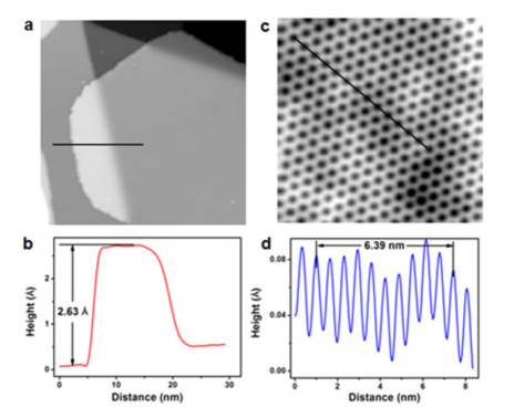
The growth of Si on Ag(111) is very sensitive to the Si coverage and the substrate temperature Kara1 . We have explored a wide range of Si coverage and substrate temperature, and several metastable phases were found at low temperature range Supplemental . On the other hand, at sufficiently high substrate temperature and small Si coverage, silicon routinely forms one-atom thick, closely packed islands which we identify as silicene sheets. Typical STM topographic image of the thus obtained monolayer islands is shown in Fig. 1(a). The line profile across the edge of a silicene island indicates that it has a height of 2.63 Å, corresponding to one atom thickness. Such islands can run across steps of the Ag(111) substrate without losing the continuity of the atomic lattice, similar to that of a graphene sheet falling on a stepped surface. As expected, the high resolution STM image in Fig. 1(c) shows a honeycomb structure reflecting the three-fold symmetry of this film. However, surprisingly, after a very careful calibration we derived a periodic constant of 0.640.01 nm (shown in line profile in Fig.1(d)), which is approximately a (a is the lattice constant of silicene, 0.38 nm, proposed in several theoretical works Liu1 ; Cahangirov ). Such a large difference is impossible a result of strain-induced lattice expansion of compression. It is most likely that we observed a ()R30∘ superstructure, which frequently shows up in three-fold symmetric systems.
To account for this observation, we have carried out first-principles calculations using the projector augmented wave (PAW) pseudopotential method and Perdew-Burke-Ernzerhof (PBE) exchange-correlation potential Pedrew implemented in the VASP package Kresse . The convergence criteria for energy and force were set to 10-5eV and 0.001eV/Å, respectively. We performed an extensive search for different geometric configurations with ()R30∘ periodicity, and concluded that a ()R30∘ superstructure cannot be stabilized in a free-standing, fully relaxed silicene model. We also considered the incorporation of Ag atoms in sites in the silicene lattice, but it was proven to be energetically unfavorable. The period constant 0.64 nm cannot also be resulting from the commensuration between the lattices of silicene and Ag(111). Actually the theoretical modeling only gives a superstructure (with respect to the 11 Ag substrate). We also exclude the possibility that the honeycomb ()R30∘ structure is simply an intervalley QPI pattern which was known in graphene to create a ()R30∘ pattern Niimi . In fact, we observed such interference pattern (to be shown in the following context), but they can be distinguished from the ()R30∘ superstructure observed here, indicating that they have different origins.

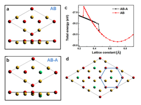
Finally, we found a clue by comparing the obtained periodicity, 0.64 nm, with the theoretically proposed values, all around 0.67 nm Liu1 ; Cahangirov ; Ding . The experimental value is about 4% smaller than the theoretical ones, indicating that the substrate may exert some influence to result in the contraction of the silicene lattice. Although the detail mechanism for such contraction still remains to be understood, for a phenomenological model we can fix the periodicity constant in a series of contracted silicene, and fully relax the inner coordinates of Si atoms. Interestingly, we found that the ()R30∘ reconstruction can indeed be stabilized in a contracted lattice. The Si atoms in previous theoretical low-buckled silicene (Fig. 2(a)) have two different heights, which we named AB configurations. To understand the experimentally observed () superstructure, we considered a configuration with extra buckling of the Si atom with planar coordinate (2/3, 2/3) downward in one () silicene unit cell, which is named ABĀ configuration, as shown in Fig. 2(b). We carried on a comprehensive study of the structure and stability of a series of contracted silicene structures from the AB and ABĀ configuration with and without small perturbation as the initial structures, respectively. Fig. 2(c) shows the structure phase transition diagram of the () superstructure and the low-buckled AB phase with minimum energy and stability, through structural optimization by keeping the periodicity constant in the contracted region. When the lattice constant is smaller than 6.25 Å, both the ABĀ configuration and the AB configuration as the initial structures return to the () superstructure (ABĀ configuration). In contrast, when the lattice constant is larger than 6.45 Å, an initial ABĀ configuration will spontaneously transfer to the low-buckled AB configuration. The superstructure (ABĀ configuration) is robust and stable when the lattice constant is smaller than 6.35 Å. Taking into account the scale error, our experimental silicene sample may be in the ABĀ phase with the () superstructure.
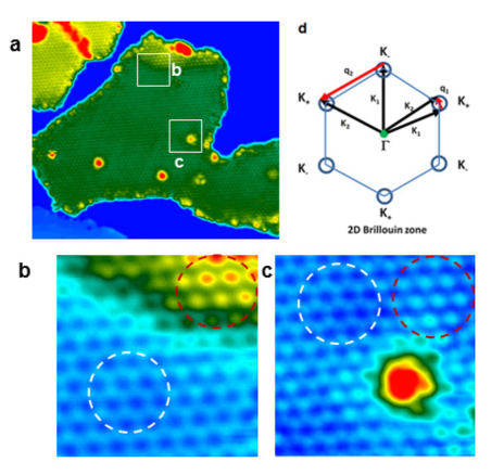
Silicene has been predicted to have Dirac-type electron structure around the Fermi energy Liu1 ; Cahangirov , similar to that of graphene. This however remains to be experimentally confirmed. On the other hand, measuring the characteristic electronic structure of our silicene film can also provide an additional proof of the basic atomic structure of our film. For graphene, the Dirac cones are located at high symmetric K points in the 2D Brillouin zone. The constant energy contours in reciprocal space cut through the electron or hole conical sheets near resulting in small circles centered at the K points (shown in Fig. 3(d)). Free carriers can be scattered within the small circles (intravalley scattering) or between circles (intervalley scattering) Rutter ; Brihuega ; Xue , resulting in QPI patterns in real space, which have been observed STS. Similar QPI patterns are expected to exist for silicene based on the same analysis.

We have observed short-wavelength interference patterns in STM images of silicene, consistent with an intervalley scattering. From Fig. 3(d) one can see that the wave vectors of intervalley scattering, , is close in length to the wave factor , which has a length of 1/ in reciprocal space, corresponding to a ()R30∘ periodicity in real space. Such a ()R30∘ interference pattern had been observed in areas near step edges and defects which serve as scattering centers, as illustrated in Fig. 3(a)-(c). The red circle in (b) is drawn near the step edge, and in (c) it is along the close-packing direction away from the point defect. Within the red circles the surface is imaged as close-packed protrusions. In contrast, within the white circles the surface is imaged as honeycomb structure, as commonly observed in large area silicene islands. Therefore, we can find a clear phase shift between the atomic corrugation and the QPI pattern, although both of them exhibit ()R30∘ periodicity. The QPI pattern originating from the scattering center extends for a length of only a few nm. Such a characteristic decaying length cannot make us assign the ()R30∘ structure observed on larger islands simply as an QPI pattern. The observation of QPI patterns, consistent with analysis based on the theoretical band structure of silicene is an additional proof that the underlying atomic structure of our film is graphene-like, with only some buckling that does not change the basic electronic structure of the film.
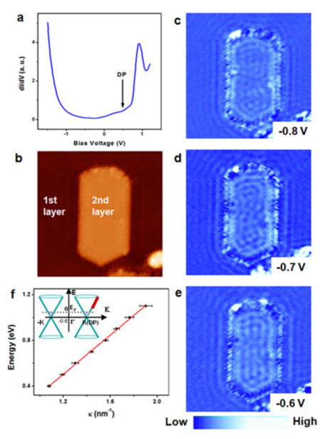
To investigate the electronic structure of silicene in more detail, we performed STS measurements (dI/dV curves and maps) on the film. Typical dI/dV curve taken at 77 K is shown in Fig.4(a). Beside the pronounced peak at 0.9 V, there is a small dip located at about 0.5 V, which is attributed to the position of Dirac point (DP) of silicene. The dip in dI/dV curve corresponding to DP is not much obvious compared with that of graphene Zhang ; Zhao , which is due to the pronounced electronic density of states (DOS) of the underlying Ag(111) substrate superimposed in the dI/dV spectra. The Fig. 4(c)-(e) are dI/dV maps of a silicene island (second layer of silicene) on the single layer of silicene, reflecting the distribution of LDOS in real space. Wave-like QPI patterns near the boundary of the island were clearly observed. The wavelength changes as a function of tip bias voltage. As the bias increases from -0.4 V to -1.1 V, the wavelength decreases correspondingly from 2.8 nm to 1.6 nm.

The 2D constant-energy contours in reciprocal space (Fig. 3(d)) are used to understand the QPI patterns. The wave factor of intravalley scattering connect points within a single constant-energy circle and determine the observed long wavelength interference pattern. In order to deduce the quasipartical energy-momentum dispersion relation, we drew E() curve in Fig. 4(f), where is the radius of constant-energy circle at K point with 2= . The values of are determined by measuring the wave length of QPI patterns in dI/dV maps. We found varied linearly with energy, with Fermi velocity m/s. The =0 energy intercept gives the Dirac energy, EF-ED = 0.520.02 eV, in consistent with the position of DP in dI/dV spectra (Fig. 4(a)) very well. The linear E- dispersion proves the existence of Dirac cone in electronic band structures of silicene. The surprising large Fermi velocity, comparable with that of graphene Rutter ; Berger , suggests the prospective applications comparable with those have been proposed or realized in graphene.
In summary, we have obtained silicene film on Ag(111) and observed an unexpected buckled superstructure. QPI patterns resulting from both intervalley and intravalley scattering were found, and the study of the linear energy-momentum dispersion and the measured Fermi velocity, as high as m/s, proves that quasiparticles in silicene behave as massless Dirac fermions. Based on these results, many further interesting studies may be proceed, including gap opening in silicene, which can realize the quantum spin Hall effect Liu1 , and high temperature electron-phonon superconductivity in hydrogenated silicene Kara2 ; Savini .
Acknowledgements: We thank Prof. Y.Q. Li and Prof. Min Qiu for helpful comments. This work was supported by the NSF of China (Grants No. 11174344, 10974231, 11174337, 11074289), and the MOST of China (Grants No. 2012CB921700, 2011CBA00100).
References
- (1) B. Aufray, A. Kara, S. Vizzini, H. Oughaddou, C. Lėandri, B. Ealet, G. L. Lay, Appl. Phys. Lett. 96, 183102(2010).
- (2) G. G. Guzmán-Verri and L. C. L. Voon, Phys. Rev. B 76, 075131 (2007)
- (3) P. D. Padova et al., Appl. Phys. Lett. 96, 261905(2010).
- (4) B. Lalmi, H. Oughaddou, H. Enriquez, A. Kara, S. Vizzini, B. Ealet, B. Aufray, Appl. Phys. Lett. 97, 223109(2010).
- (5) C. C. Liu, W. X. Feng, Y. G. Yao, Phys. Rev. Lett. 107, 076802(2011).
- (6) S. Cahangirov, M. Topsakal, E. Akturk, H. Sahin, S. Ciraci, Phys. Rev. Lett. 102, 236804(2009).
- (7) K. Takeda and K. Shiraishi, Phys. Rev. B 50, 14916(1994).
- (8) A. K. Geim, K. S. Novoselov, Nature Mater. 6, 183(2007).
- (9) A. H. Castro Neto, F. Guinea, N. M. R. Peres, K. S. Novoselov, A. K. Geim, Rev. Mod. Phys. 81, 109(2009).
- (10) C. L. Kane, E. J. Mele, Phys. Rev. Lett. 95, 226801(2005).
- (11) C. C. Liu, H. Jiang, Y. G. Yao, Phys. Rev. B 84, 195430(2011).
- (12) B. A. Bernevig, T. L. Hughes, and S. C. Zhang, Science 314, 1757(2006).
- (13) Y.Takamura, private communication.
- (14) A. Kara, H. Enriquez, A. P. Seitsonen, L. C. Lew Yan Voon, S. Vizzini, B. Aufray, H. Oughaddou, Surf. Sci. Rep. 67, 1(2012).
- (15) See Supplemental Materials at http://.
- (16) J. P. Perdew, K. Burke, M. Ernzerhof, Phys. Rev. Lett. 77, 3865(1996).
- (17) G. Kresse J. Furthmüller, Phys. Rev. B 54, 11169(1996).
- (18) Y. Niimi, T. Matshui, H. Kambara, K. Tagami, M. Tsukada, H. Fukuyama, Phys. Rev. B 73, 085421(2006).
- (19) Y. Ding, J. Ni, Appl. Phys. Letts. 95, 083115(2009).
- (20) G. M. Rutter, J. N. Crain, N. P. Guisinger, T. Li, P. N. First, J. A. Stroscio, Science 317, 219(2007).
- (21) I. Brihuega et al., Phys. Rev. Letts. 101, 206802(2008).
- (22) J. Xue, J. Sanchez-Yamagishi, K. Watanabe, T, Taniguchi, P. Jarillo-Herrero, B. J. LeRoy, Phys. Rev. Letts. 108, 016801(2012).
- (23) Y. B. Zhang, V. W. Brar, F. Wang, C. Girit, Y. Yayon, M. Panlasigui, A. Zettl, M. F. Crommie, Nature Phys. 4, 627(2008).
- (24) L. Zhao et al., Science 333, 999(2011).
- (25) C. Berger et al., Science 312, 1191(2006).
- (26) A. Kara, C. Leandri, M. E. Davila, P. De Padova, B. Ealet, H. Oughaddou, B. Aufray, G. Le Lay, J. Supercond. Nov. Magn. 22, 259(2009).
- (27) G. Savini, A. C. Ferrari, F. Giustino, Phys. Rev. Letts. 105, 037002(2010).