Crossover from spin accumulation into interface states to spin injection in the germanium conduction band
Abstract
Electrical spin injection into semiconductors paves the way for exploring new phenomena in the area of spin physics and new generations of spintronic devices. However the exact role of interface states in spin injection mechanism from a magnetic tunnel junction into a semiconductor is still under debate. In this letter, we demonstrate a clear transition from spin accumulation into interface states to spin injection in the conduction band of -Ge. We observe spin signal amplification at low temperature due to spin accumulation into interface states followed by a clear transition towards spin injection in the conduction band from 200 K up to room temperature. In this regime, the spin signal is reduced down to a value compatible with spin diffusion model. More interestingly, we demonstrate in this regime a significant modulation of the spin signal by spin pumping generated by ferromagnetic resonance and also by applying a back-gate voltage which are clear manifestations of spin current and accumulation in the germanium conduction band.
pacs:
72.25.Hg, 72.25.Mk, 85.75.-d, 73.40.Gk, 72.25.DcThe first challenging requirement to develop semiconductor (SC) spintronicsZutic2004 ; Awschalom2007 i.e. using both carrier charge and spin in electronic devices consists in injecting spin polarized electrons in the conduction band of a SC at room temperature. SCs should be further compatible with silicon mainstream technology for implementation in microelectronics making silicon, germanium and their alloys among the best candidatesZutic2011 . In Si, due to low spin-orbit coupling, very long spin diffusion lengths were predicted and measured experimentallyDash2009 ; Jonker2007 ; Appelbaum2007 ; Suzuki2011 . Germanium exhibits the same crystal inversion symmetry as Si, low amount of nuclear spins but higher carrier mobility and larger spin-orbit coupling which should allow in principle spin manipulation by electric fields such as the Rashba fieldZhou2011 ; Jain2011 ; Saito2011 ; Jeon2011 . Beyond the conductivity mismatch issueFert2001 , another obstacle to electrical spin injection in SCs is the presence of localized states at the interface between the injecting electrode and the SCDash2009 ; Jain2011 ; Tran2009 . Their exact role in spin injection mechanism and their existence itself need to be elucidated before achieving efficient spin injection in SCs. In this work, we demonstrate a clear transition from spin accumulation into interface states to spin injection in the conduction band of -Ge. We first observe spin signal amplification at low temperature due to spin accumulation into interface states followed by a clear transition towards spin injection in the conduction band from 200 K up to room temperature. In this regime, the spin signal is reduced down to a value compatible with spin diffusion model. Moreover we demonstrate in this regime a significant modulation of the spin signal by spin pumping generated by ferromagnetic resonance and also by applying a back-gate voltage which are clear manifestations of spin current and accumulation in the conduction band of -Ge.

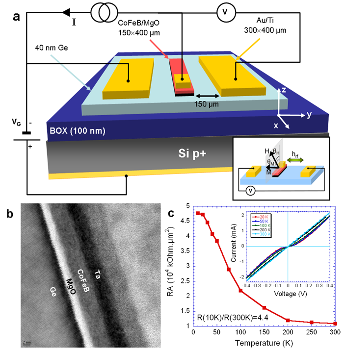
The multi-terminal device we used for electrical measurements is shown in Fig. 1a. The full stack Ta(5 nm)/Co60Fe20B20(5 nm)/MgO(3 nm) has been grown by sputtering and annealed on Germanium-On-Insulator (GOI) wafersJain2011 ; note1 (Fig. 1b). We have inserted a thin MgO tunnel barrier to circumvent the conductivity mismatch and partly alleviate the Fermi level pinning by reducing the interface states densityCantoni2011 ; Lee2010 ; Zhou2010 which leads to a modest Schottky barrier height at the MgO/-Ge interface. Conventional optical lithography was used to define 3-terminal devices made of a tunnel spin injector in between two ohmic contacts made of Au(250 nm)/Ti(10 nm). Fig. 1c displays the tunnel junction product and the corresponding curves at different temperatures. We first observe clear non-linear symmetric characteristics which confirms that tunnelling transport takes place in our junctions. Furthermore the product only varies by a factor 4.4 between 10 K and 300 K again in good agreement with tunnelling dominated transport. It exhibits a transition to low values above 200 K. The 30 nm-thick Ge channel exhibits a metallic character with its resistivity increasing by 18.7 % with temperature and reaching 3.7 m.cm at room temperature. The associated electron mobility is of the order of 1700 cm2.V-1.s-1.

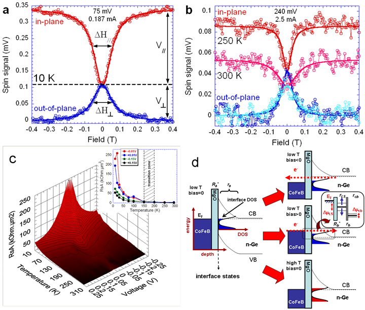
Electrical spin injection/detection measurements have been performed at different temperatures and bias voltages using the contacts geometry displayed in Fig. 1a. Spin detection is achieved by Hanle measurements that probe spin accumulation at the ferromagnet/SC interface. In comparison, inverse spin Hall effect (ISHE) and gate effect presented in the second part of this letter are sensitive to spin accumulation far from the interface in the germanium conduction band. The 3-terminal geometry in which the same electrode is used for spin injection and detection, represents a unique tool to probe spin accumulation both into interface states and in the channel. In Fig. 2a and 2b, the magnetic field was applied out-of-plane along to obtain Hanle curves (: spin precession around the applied field) and in-plane along to obtain inverted-Hanle curves (: to suppress spin precession around interface random fields)Dash2011 . In that case, the total spin signal scaling with the full spin accumulation is given by: and the spin resistance-area product by: where is the applied current and the ferromagnetic electrode area. All our measurements of the total spin signal have been gathered into a single 3D plot in Fig. 2c that clearly demonstrates spin signal amplification at low bias and below 150 K. This spin amplification is usually attributed to sequential tunnelling through localized states at the MgO/Ge interfaceDash2009 ; Jain2011 ; Tran2009 due to spin confinement by the reminiscent Schottky barrier. Using the same spin diffusion model as in Ref. Tran2009 , spin accumulations into localized states and in the Ge conduction band are respectively given by (see Fig. 2d and Ref. note2 ):
It should be underlined here that these expressions are only valid in the case of a two-step tunneling process through interface states. 0.65 is the tunnel spin polarization estimated from the Jullière’s formulaJulliere1975 on a symmetric magnetic tunnel junction CoFeB/MgO/CoFeB at room temperature and is the current density. The spin accumulation is related to the experimental spin signal through the expression: (Ref. Dash2009 ). Both spin amplification and spin injection in the conduction band depend on the relative intensity of , and as well as on their temperature and bias voltage dependence. As shown in Fig. 2d, at low temperature and low bias voltage, the two-dimensional density of states (2D-DOS) of localized states at the Fermi level is low () so that , and the spin-current leakage from the localized states to the conduction band through the Schottky barrier is very weak () leading to . Hence we find: (spin signal amplification due to spin accumulation into interface states) and (spin accumulation in the Ge conduction band is negligibly small and only spin accumulation into interface states is detected). Still at low temperature but now at finite bias voltage as shown in Fig. 2d, sequential tunnelling takes place through much higher interface 2D-DOS leading to a drastic reduction of and . In the same way, by increasing the temperature, electrons may tunnel through higher energy levels at the interface where the 2D-DOS is much higher which also reduces and (see Fig. 2d). We then infer that the spin signal transition we observe between 150 K and 200 K is due to the progressive decrease of with temperature (due to thermally activated electrical transport over the Schottky barrier) as pointed out in ref. Jain2011 and experimentally observed in the temperature dependence of the product (Fig. 1c). Assuming in the whole temperature range which is quite fair regarding the difference in 2D-DOSMatsubara2008 ( 1011-1012 cm-2.eV1014 cm-2.eV-1) we propose the following scenario: i) for T150 K, , and 0 as discussed previously, ii) for 150 KT200 K, , and : we still observe spin signal amplification but spins start to accumulate in the Ge conduction band partly due to a shorter carrier tunnelling transfer time from localized states into the -Ge conduction band and iii) for T200 K, , , interface states progressively couple to the Ge conduction band and a significant spin accumulation now takes place in the channel. The observation of inverse spin Hall effect (ISHE) by spin pumping together with the observation of spin signal modulation upon the application of a gate voltage for temperatures higher than 200 K clearly support this scenario.

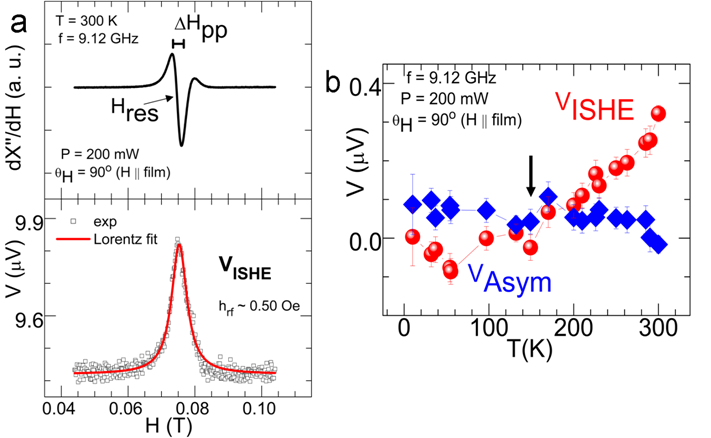
As shown in Fig. 3a, by measuring simultaneously the voltage between the Au/Ti ohmic contacts and the ferromagnetic resonance (FMR) spectrum of Ta/CoFeB/MgO/Ge we are able to investigate spin injection in Ge via the inverse spin Hall effect (ISHE) at zero bias voltageSaitoh2006 ; Vila2007 ; Ando2011a ; Ando2011b . For this purpose, the same device as the one previously used for electrical measurements is introduced into a Brker X-band cavity and the measuring geometry is shown in the inset of Fig. 1a. All the measurements presented in Fig. 3 have been performed with the static magnetic field applied along (=90∘) i.e. along the CoFeB bar. Under radiofrequency excitation the magnetization precession in the ferromagnetic layer pumps spins to the non-magnetic Ge layer and the corresponding spin current generates an electric field in Ge due to ISHE: where is the spin-current density along and its spin polarization vector. This electric field converts into a voltage between both ends of the Ge channel. The microwave frequency was =9.12 GHz and we could observe the voltage signal due to ISHE at room temperature (Fig. 3a) and easily fit it using a symmetrical Lorentzian curve. This symmetric voltage coincides with the main FMR line at =0.074 Tnote3 . This result clearly demonstrates the presence of both spin accumulation and related spin current in the Ge conduction band at room temperature. Furthermore we have shown that all our findings are in good agreement with the observation of ISHE: symmetrical behaviour of around the resonance field , =0 when the external magnetic field is applied perpendicular to the film (=0), changes its sign when crossing =0 and finally the linear dependence of its amplitude with the microwave power excitationRojas2012 . From at room temperature, we adapted a model based on the spin mixing conductance formalismTserkovnyak2005 already used in metalsMosendz2010 and semiconductors with a Schottky contactAndo2011b ; Ando2012 to estimate the spin Hall angle in -Ge: 0.002 (see Supplemental Material). We found similar spin Hall angles on several devices. This model is probably not the most appropriate and should be reconsidered in the case of Ferromagnet/Oxide/SC systems but it gives a reasonable value for in Ge. This is indeed of the same order of magnitude as in -GaAs (0.007 in Ref. Ando2011b ) and one order of magnitude larger than in -Si (0.0001 in Ref. Ando2012 ). We have then investigated the temperature dependence of ISHE. For this purpose, the voltage corresponding to the main FMR peak has been fitted using both symmetric and asymmetric contributions. They are reported as a function of temperature in Fig. 3b. The symmetric signal is related to ISHE while the asymmetric one may be due to reminiscent rectification effects as a combination of radiofrequency eddy currents and anisotropic magnetoresistance (AMR) in CoFeBMosendz2010b ; Azevedo2011 . Increasing the temperature, we clearly see a transition with the appearance of ISHE at approximately 150 K which is in perfect agreement with the transition from spin accumulation into interface states to the -Ge conduction band discussed previously. The asymmetric voltage contribution remains negligible and almost constant within error bars in the whole temperature range.

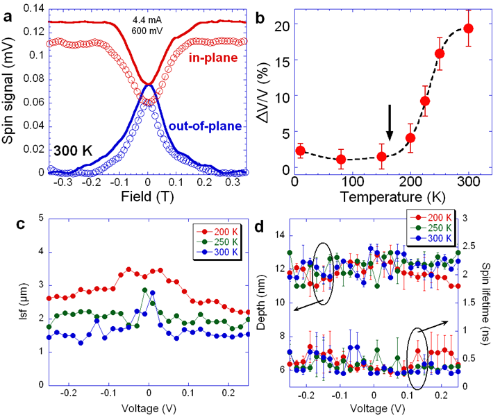
Using the field-effect transistor structure, we now focus on the application of a gate voltage to the Ge channel to modulate the spin signalAndo2011c . At negative gate voltage to a maximum of =-50 V, the carrier density is lowered in the -Ge channel and its resistivity is enhancednote4 . At 10 K, we find: /=(-50V)-(0V)/(0V)=+68.2 % whereas /=+21.9 % at 300 K. The resulting spin signal variation at 300 K is reported in Fig. 4a. We can clearly see the effect of the gate voltage with a significant spin signal increase whereas almost no variation is observed at 10 K (not shown). All the measurements are summarized in Fig. 4b as a function of temperature: a clear transition occurs again between 150 K and 200 K (171 K from a linear fit to the finite values of / above 200 K). Again these findings are in good agreement with a transition from spin injection into interface states to the Ge conduction band. To be more quantitative, in the case of spin injection in the Ge conduction band and in the frame of the diffusive regime modelFert2001 , the spin resistance-area product is given by: . Hence if we assume that and remain constant under the application of an electric field, scales as which is proportional to the channel resistance . We thus expect / to scale with / in the event that spin polarized carriers are injected in the Ge conduction band. Below 150 K, we obtain negligible values of / for large values of / which is compatible with spin accumulation into interface states. Above 200 K, / starts to increase as spins start to accumulate in the Ge conduction band and at room temperature we find // which means that we fully achieved spin injection in the Ge conduction band.
Based on the results we obtained in spin pumping and electric field effect measurements, we can now estimate from the experimental spin resistance-area product as well as from the fit of Hanle and inverted Hanle curves. In Fig. 4c, we have converted the spin resistance-area product into using the spin diffusion modelFert2001 : at T=200 K, 250 K and 300 K. At room temperature, we find 1.5 m with weak bias voltage dependence up to 0.5 V. Moreover in Hanle and inverted Hanle measurements, spins that are injected electrically precess around the external magnetic field (either along or ) and random fields created by surface charges. Random fields are calculated from the surface roughness parameters given by atomic force microscopy (AFM) performed on the whole stack Ta/CoFeB/MgO/Ge. We found a root-mean-square (RMS) roughness of 0.2 nm and a correlation length of 40 nm. Then the spin dynamics has been computed by considering only spin precession and relaxation: spin drift and diffusion were neglected as discussed in Ref. Dash2011 . Finally a triple fit over =/, and yields the mean depth at which spin polarized electrons are injected and . The results are displayed in Fig. 4d and are almost the same for all three temperatures: 200 K, 250 K and 300 K with very weak bias voltage dependence. In average, spin polarized electrons are injected 10 nm deep into the Ge film and =400100 ps at room temperature. Using =43 cm2.s-1, we find: =1.30.2 m at room temperature which is in very good agreement with the value obtained from the spin resistance-area product.
In summary, we have demonstrated a clear crossover from spin accumulation into interface states that leads to spin signal amplification to spin injection in the Ge conduction band at 200 K. For that purpose, we have shown inverse spin Hall effect in Ge and spin signal modulation applying a back gate voltage from 200 K up to room temperature. From a general point of view, we believe that the same transition should be observable in any low gap semiconductors in the presence of interface states.
This work was supported by the Nanoscience Foundation of Grenoble through the RTRA project IMAGE. The initial GOI substrates were obtained through the collaboration with Soitec under the public funded NanoSmart program (French OSEO).
References
- (1) I. Zutic, J. Fabian, and S. Das Sarma, Rev. Mod. Phys. 76, 323 (2004).
- (2) D. D. Awschalom and M. E. Flatté, Nature Phys. 3, 153 (2007).
- (3) I. Zutic and H. Dery, Nature Mater. 10, 647 (2011).
- (4) S. P. Dash, S. Sharma, R. S. Patel, M. P. de Jong, and R. Jansen, Nature 462, 491 (2009).
- (5) B. T. Jonker, G. Kioseoglou, A. T. Hanbicki, C. H. Li, and P. E. Thompson, Nature Phys. 3, 542 (2007).
- (6) I. Appelbaum, B. Huang, and D. J. Monsma, Nature 447, 295 (2007).
- (7) T. Suzuki et al., Appl. Phys. Exp. 4, 023003 (2011).
- (8) Y. Zhou et al., Phys. Rev. B 84, 125323 (2011).
- (9) A. Jain et al., Appl. Phys. Lett. 99, 162102 (2011).
- (10) H. Saito et al., Solid State Comm. 151, 1159 (2011).
- (11) K. R. Jeon et al., Phys. Rev. B 84, 165315 (2011).
- (12) A. Fert and H. Jaffrès, Phys. Rev. B 64, 184420 (2001).
- (13) M. Tran et al., Phys. Rev. Lett. 102, 036601 (2009).
- (14) The Ge layer has been P-implanted in two steps: the 30 nm-thick Ge bottom layer is n-doped at 1018 cm-3 and the 10 nm-thick top layer is n+-doped (1019 cm-3) to make the Schottky barrier transparent. At the end of the device process, the top n+-doped layer has been removed by soft argon etching.
- (15) M. Cantoni, D. Petti, C. Rinaldi, and R. Bertacco, Appl. Phys. Lett. 98, 032104 (2011).
- (16) D. Lee et al., Appl. Phys. Lett. 96, 052514 (2010).
- (17) Y. Zhou et al., Appl. Phys. Lett. 96, 102103 (2010).
- (18) S. P. Dash et al., Phys. Rev. B 84, 054410 (2011).
- (19) C. H. Li, O. M. J. van’t Erve, and B. T. Jonker, Nature Comm. 2, 245 (2011).
- (20) H. Matsubara, T. Sasada, M. Takenaka, and S. Takagi, Appl. Phys. Lett. 93, 032104 (2008).
- (21) N. Taoka et al., Appl. Phys. Lett. 109, 084508 (2011).
- (22) and = are the tunnel and Schottky resistances respectively. and (resp. and ) are the spin accumulation and spin resistance of localized interface states (resp. Ge conduction band). is the characteristic leakage time from localized states to the Ge conduction band and depends on the Schottky barrier height and width, is the two-dimensional density of states (2D-DOS) at the MgO/Ge interface, is the spin lifetime of electrons into localized states, the channel resistivity and (resp. ) the spin diffusion length (resp. spin lifetime) of electrons in -Ge. is the 2D-DOS in the Ge conduction band.
- (23) M. Jullière, Phys. Lett. 54A, 225 (1975).
- (24) E. Saitoh, M. Ueda, H. Miyajima, and G. Tatara, Appl. Phys. Lett. 88, 182509 (2006).
- (25) L. Vila, T. Kimura, and Y. C. Otani, Phys. Rev. Lett. 99, 226604 (2007).
- (26) K. Ando et al., J. Appl. Phys. 109, 103913 (2011).
- (27) K. Ando et al., Nature Mater. 10, 655 (2011).
- (28) A second but very weak FMR line appears in some devices as the one of Fig. 3a at =0.077 T. This resonance peak systematically gives a weak asymmetric voltage contribution that decreases with temperature. The origin of this secondary peak is not investigated in this paper.
- (29) J.-C. Rojas-Sanchez et al., submitted to Phys. Rev. B (2012).
- (30) Y. Tserkovnyak, A. Brataas, G. E. W. Bauer, and B. I. Halperin, Rev. Mod. Phys. 77, 1375 (2005).
- (31) O. Mosendz, J. E. Pearson, F. Y. Fradin, S. D. Bader and A. Hoffmann, Appl. Phys. Lett. 96, 022502 (2010).
- (32) K. Ando and E. Saitoh, Nature Comm. 3:629 doi: 10.1038/ncomms 1640 (2012).
- (33) O. Mosendz et al., Phys. Rev. B 82, 214403 (2010).
- (34) A. Azevedo, L. H. Vilela-Leão, R. L. Rodriguez-Suárez, A. F. Lacerda Santos, and S. M. Rezende, Phys. Rev. B 83, 144402 (2011).
- (35) Y. Ando at al., Appl. Phys. Lett. 99, 132511 (2011).
- (36) The field-effect transistor exhibits non-symmetric behavior and at positive gate voltage (up to =50 V) the channel resistivity remains almost unchanged. We have also performed non-local measurements to probe the interface resistance under the application of a gate voltage. For positive and negative gate voltage, we found the same interface resistance.