The Nature of Electronic States in Atomically Thin MoS2 Field-Effect Transistors
Abstract
We present low temperature electrical transport experiments in five field effect transistor devices consisting of monolayer, bilayer and trilayer MoS2 films, mechanically exfoliated onto Si/SiO2 substrate. Our experiments reveal that the electronic states in all films are localized well up to the room temperature over the experimentally accessible range of gate voltage. This manifests in two dimensional (2D) variable range hopping (VRH) at high temperatures, while below K the conductivity displays oscillatory structures in gate voltage arising from resonant tunneling at the localized sites. From the correlation energy () of VRH and gate voltage dependence of conductivity, we suggest that Coulomb potential from trapped charges in the substrate are the dominant source of disorder in MoS2 field effect devices, which leads to carrier localization as well.
KEYWORDS: Dichalcogenides. Field effect transistor. MoS2. Localization. Mott variable range hopping. Resonant tunneling. Charge impurity scattering.
MoS2-based dichalcogenides have recently been of renewed interest due to the possibility of creating atomically thin semiconductor membranes for a variety of applications. 1, 2, 3, 4 Being a layered compound, with a weak van der Waal interaction between the layers, MoS2 can be exfoliated like graphene on insulating substrates. This has recently led to the fabrication of single-layer MoS2 field effect transistor that has a very high on-off ratio due to a finite bandgap. 4 It has been demonstrated that the bandgap is indirect ( eV) for multilayer MoS2 films but direct ( eV) for single atomic layer, 3 which may lead not only to low-power dissipation electronic devices, but also new possibilities in energy harvesting designs. The existence of bandgap can also have serious implications on the charge transport and nature of disorder in MoS2 films, affecting its ability to screen external potential fluctuations. 5, 6 In fact, the mobility ( cm2/V.s) of charge carriers in single layer MoS2 devices is much lower than graphene , which has been attributed to the absence of a bandgap in pristine 2D layers of graphene. Our objective here is to explore the nature of disorder, and hence that of the electronic states, from the low temperature electrical transport in MoS2 films, when the film thickness is downsized from few to a single molecular layer.
Often, disorder in low dimensional electron systems arises from extraneous sources, such as local charge distribution that induces a random Coulomb potential on the electrons. This, for example, can be the remote dopant ions in modulation-doped III-V semiconductor, 7 or charges trapped in the substrate in case of graphene. 8 At low carrier densities the screening of the random Coulomb potential becomes weak, causing carriers to localization and/or charge distribution to become inhomogeneous. 9, 10 This would not only have a direct impact on the transport, but also on the response of the system to various stimuli including light, stress . Although a similar charge trap-mediated transport has been suggested in thick nanoscale patches of MoS2, 11 the microscopic picture is far from clear. It is also not known if such a picture would be valid in mono or very few layer MoS2 devices. In this context, our experiments with MoS2 devices of different thicknesses (see Table I) reveal that electrons are strongly localized in all cases which manifest in variable range hopping transport and an inhomogeniety in charge distribution that results in local transport resonances at low temperatures. We suggest that localization is probably due to strong potential fluctuations induced by the randomly occupied charge traps that are located primarily at the MoS2-substrate interface.
| Device | Number of layer | Contact material | 111in V | Device area (LW)222both dimensions in m | Mobility333in cm2/V-s near room temperature |
| MoS1La | 1 | Ti/Au | 32 | 1 | |
| MoS1Lb | 1 | Au | 15 | 5 | |
| MoS1Lc | 1 | Au | -5 | 12 | |
| MoS2L | 2 | Au | -2 | 20 | |
| MoS3L | 3 | Ti/Au | -25 | 10 |
RESULTS AND DISCUSSION
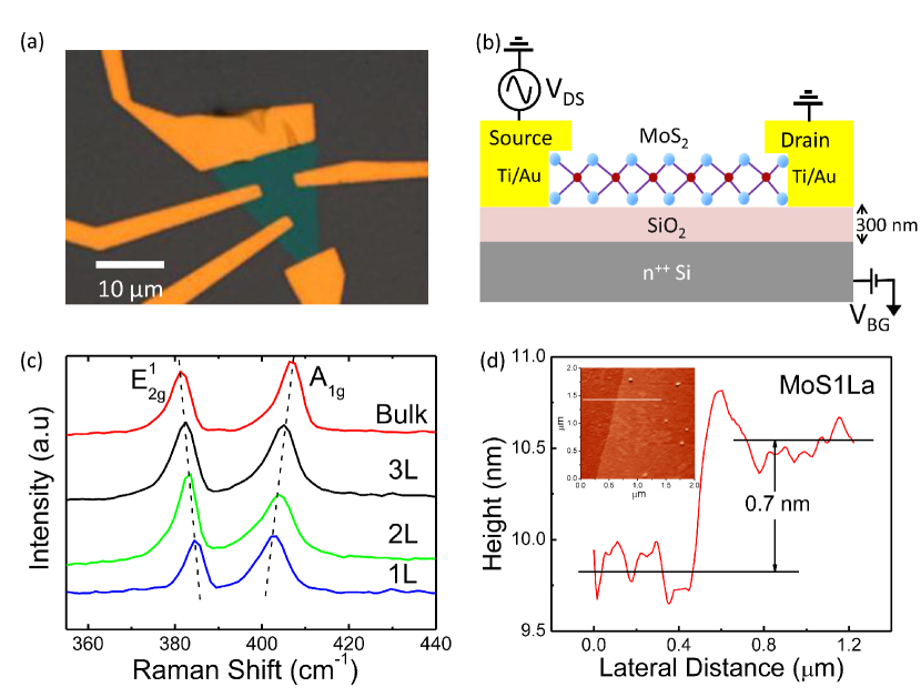
Devices were prepared by standard mechanical exfoliation of bulk MoS2 on 300 nm SiO2 on doped silicon substrate using scotch tape technique. 12, 13 The flakes were identified using optical microscope and characterized Raman spectroscopy and atomic force microscopy (AFM). We present detailed experiments on five devices (See Table I) of different film thicknesses. In Fig. 1c we show Raman spectra for bulk, tri and single layer MoS2 films. We focus on the E and A1g modes which have been shown to be sensitive to the number of atomic layers. 3 The position of both modes agree well with recent investigation of Raman spectroscopy in thin exfoliated MoS2 films. The separation of E and A1g peaks were found to be 23 cm-1, 21 cm-1 and 16 -18 cm-1 for tri, bi and single layer respectively. For further confirmation of Raman data, we determined the thickness of flakes using contact mode AFM. A line scan across the edge of a single layer flake (Fig. 1d) shows a step of nm which compares very well with the thickness of the single MoS2 layer ( nm).
The electrical contacts, designed with electron beam lithography, consisted of thermally evaporated Ti/Au or Au films. The optical image of the MoS3L device is shown in Fig. 1a. All measurements were carried out in cryostats under high vacuum ( mbar) condition. In all devices the gate voltage () was applied only at the doped silicon backgate (see Fig. 1b). Measurements were primarily two-probe current measurement using lockin technique due to very high resistance of these systems, although four-probe devices were fabricated as well. We found, at high doping concentration, the contact resistance was negligible near room temperature, but increases to about half of sample resistance below 100K. Detailed measurements, where and are the drain-source current and bias respectively, were conducted to characterize the electrical contacts (see supplementary information). At low voltages ( mV), at all and near room temperature, were linear for both Ti/Au and Au deposited samples although we have got better linear contact with only Au. These results bear close resemblance to the characteristics reported recently for high mobility MoS2 devices. 4 As shown in the supplementary information, characteristics become nonlinear at large , particularly at low temperatures (), although we attribute this to the insulating nature of the devices which causes the nonlinearity. The symmetric nature of - around enables us to eliminate any possibility of Schottky contact in our operating range. This is supported by the observed magnitude of the differential carrier mobility , where is the gate capacitance per unit area (here F/m2 for 300 nm SiO2), and is the linear conductivity at low . and are the length and width of the MoS2 channel. In both two and four-probe geometry, we obtained similar values of mobility, which are typical values reported for MoS2 transistors 4 on SiO2 substrate (See Table I).
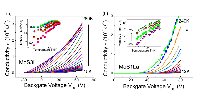
In Fig. 2 we show the variation of in MoS3L and MoS1La as a function of over a range K to 280 K. The conduction was achieved predominantly in the positive regime implying that the MoS2 films were intrinsically -type. 11 The doping was higher in MoS3L which required a negative to pinch-off completely. Below K both devices were strongly insulating at all . A weak metal-like behavior was observed at K and very high doping (large positive ) for most of the samples. Such a behavior, which was stronger in MoS3L, was found to be connected to a decrease in with increasing in this regime (inset of Figs. 2a and 2b). This can be attributed to enhanced scattering of electrons by phonons at high temperatures. 14 At low , both and drop rapidly with decreasing . Such an insulating behavior was observed in multilayer nanopatches of MoS2 (thickness: 8 35 nm) as well, 11 with an apparent activated behavior of over a rather limited range of . This was explained by invoking a dense distribution of trap states, which acted as an “impurity band”, although the origin or the physical location of such traps are unclear.
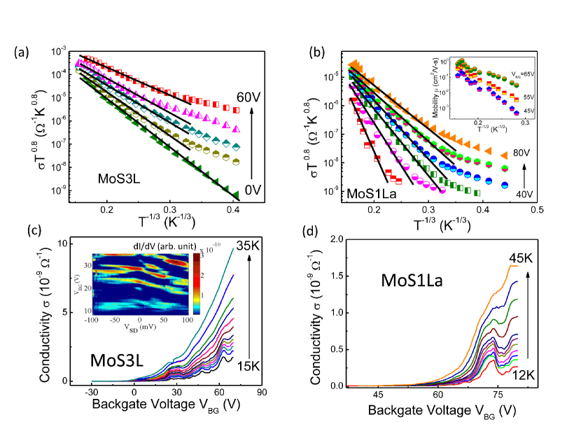
In contrast to the nanopatches, 11 the -dependence of in our mono and trilayer MoS2 devices are not activated, but there are two distinct regimes in the -variation in (Figs. 3a and 3b): The high- regime ( K), where increases rapidly with increasing , and second, the low- regime ( K), where the variation in weakens considerably at most in both devices (except for MoS1La at low , where the weakening of sets in at higher (Fig. 3b)). We find that in the high regime, the variation of with can be modeled very well in terms of variable range hopping (VRH) transport rather than the thermally activated behaviour with
| (1) |
where and are correlation energy scale and dimensionality, 15, 16 respectively, and with . The agreement of the data to VRH transport with indicates the electron transport in atomically thin MoS2 to occur in a wide () band of localized states, rather than direct excitation to conduction band minimum or mobility edge from the Fermi energy as suggested for the nanopatches. 17 The VRH transport in also results in in two dimension. 14 This is confirmed in the inset of Fig. 3b for the MoS1La device. The magnitude of decreases rapidly as , or equivalently, the Fermi energy , is increased. Such a behavior is common to strongly localized 2D electron systems, 18, 19 and implies that is located in the conduction band tail.
To understand the weakening of at K, we have magnified this regime for both MoS3L (Fig. 3c) and MoS1La (Fig. 3d). In both cases, the variation of with becomes nonmonotonic, and displays several peaks which become progressively well defined as is reduced. The peaks are highly reproducible, and stable even at K, indicating that random fluctuations due to interference of hopping paths are unlikely to cause them. Resonant tunneling at the localized states in disordered mesoscopic semiconductors is known to result in strong reproducible peaks in at low temperatures. 20, 21 In the presence of multiple overlapping resonances, dependence of weakens as observed in our data. 21 However, confirmation of this scenario can be obtained by shifting the resonance peaks using finite . For this, we focused on a small interval of ( V) near pinch-off where a number of isolated resonances could be identified. In the plane, this leads to diamond-like pattern in differential conductivity (Inset: Fig 3c). The occurrence of transport resonances indicates a rather inhomogenous charge distribution in MoS2 films, possibly puddles of charge near conduction threshold, through which charging events at the localized states couple to the metal contacts.
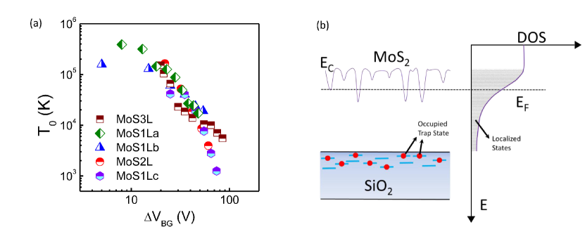
We now turn into the key issue here that concerns the origin of localized states in ultrathin MoS2 films. This requires an understanding of the origin of disorder in such systems, for which we first examine the values of . However, to compare for different devices, we define a device-specific reference voltage close to the “pinch-off” voltage in curve, so that the difference is proportional to or number density . In Fig. 4a, we have plotted the variation of as a function of for all the devices. The striking feature here is the close agreement of in both absolute magnitude and energy over nearly three decades, irrespective of independent preparation of devices, varying layer number, mobility and device geometry . This indicates a very similar disorder landscape in all devices that reflects comparable magnitude and energy dependence of localization length and density of states . Disorder arising from defects in bulk of the MoS2 films are unlikely to explain the insensitivity of to number of layers since screening of impurities and density of defect in bulk are expected to strongly influence the density of localized states. In stead, our data indicates a common external origin of disorder, such as the trapped charges in the substrate. This is also supported by recent transport experiments, 4 where higher mobility of thin MoS2 flakes could be achieved by changing electrostatic environment alone. Indeed a charge trap-induced disorder can readly explains the observed magnitude of . To illustrate this we take as the typical size of the puddles, which for MoS3L can be roughly estimated to be nm from the charging energy ( meV) at V (corresponding to V) (See inset of Fig. 3c). Taking eV-1cm-2 as the typical surface density of charge traps at SiO2 interface, 11, 22 and using , we find K, which is in good agreement to the observed magnitude from VRH data (Fig. 4a).
This leads us to suggest that the physical origin of the localized states in ultra-thin MoS2 films is connected to the random potential fluctuations from the trapped charges at the MoS2-SiO2 interface. (See the schematic of Fig. 4b.) The screening of these trapped charges will be poor due to the large bandgap of MoS2 (unlike graphene) and hence can lead to a considerably long band tail. It is likely that the interfacial traps are randomly occupied during processing of the devices, predominantly transfer of electrons from the exfoliated prestine MoS2 layers, and subsequently form the frozen disorder landscape since most experiments are conducted at low .
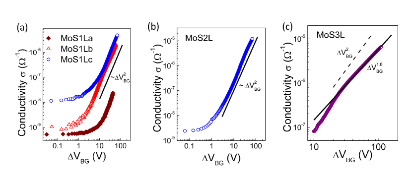
Finally to confirm the charge impurity induced disorder, we have examined the nature of scattering of carriers by defects at high and so that the electron wavefunctions are nearly extended. If the main source of disorder arises from the randomly occupied interfacial traps, one would expect the scattering to be dominated by charge impurity scattering, which for two-dimensional electron systems with parabolic energy bands will lead to, 23
| (2) | |||||
| (3) |
In Fig. 5a, b and c, we have shown the dependence of on () near room temperature, for the single, bi and tri layer MoS2 devices, respectively. In all monolayer MoS2 devices, as well as the bilayer (MoS2L) case, we find indicating scattering from nearly unscreened charged impurities. In the trilayer device (MoS3L), the variation in is somewhat slower, indicating partial screening of the charge impurities. Assuming the electronic density of states to be approximately one-tenth of the free electron density of states at maximal doping used in our experiment the Debye screening length in our devices can be estimated to be , which is nearly three molecular layers of MoS2. This readily explains the bare charge impurity scattering in single and bi-layer MoS2, while charge impurities are partially screened for the trilayer device.
It is then natural to draw an analogy of our findings to other heavily researched exfoliated atomic scale transistors in particular, graphene and topological insulators. The ubiquity of surface trap states probably constitutes a generic source of disorder in such ultra-thin field effect devices. Reducing substrate traps, for example, by using crystalline substrates such as graphene on boron nitride, may improve the quality of these systems considerably. A suspended device, as in case of graphene, could also lead to extremely high mobilities.
CONCLUSION
We have studied low temperature electrical transport in mono, bi and trilayer MoS2 transistor exfoliated onto Si/SiO2 substrates. We find that the electrons in all cases are localized well upto room temperature at most gate voltages, and displays variable range hopping transport as temperature is lowered. We showed that the disorder is likely to arise from Coulomb potential of randomly distributed charges at the MoS2-SiO2 interface, and hence highly improved devices should be possible with appropriate substrate engineering.
METHODS
Device Fabrication
MoS2 flakes were exfoliated from bulk MoS2 (SPI Supplies) using scotch tape on SiO2 (300 nm)/n++ Si wafer. To keep the disorder level comparable, the wafers were thoroughly cleaned by standard RCA cleaning followed by acetone and isopropyl alcohol cleaning in ultrasonic bath. The flakes with typical linear dimensions ranging from 2 m to 20 m were identified by Olympus BX51 optical microscope. Raman spectrum are recorded using WITEC confocal (X100 objective) spectrometer with 600 lines/mm grating, 514.5 nm excitation at a very low laser power level (less than 1 mW) to avoid any heating effect. The AFM measurements were carried out in contact mode with a NT-MDT NTEGRA AFM instrument. Ti(10 nm)/Au(40 nm) or Au(40 nm) contacts were defined using standard electron beam lithography followed by thermal evaporation and lift off in hot acetone. No Ar/H2 annealing was done in any of our devices.
Acknowledgement. We acknowledge Department of science and Technology (DST) for a funded project. S.G. and A.N.P. thank CSIR for financial support.
Supporting Information Available. Detail room temperature and low temperature drain source characteristics are presented for trilayer and monolayer devices in Figure S1. The temperature dependent data for Mott type variable range hopping for MoS1Lc is shown in Figure S2 along with the calculation of VRH slope. This material is available free of charge a the Internet at http://pubs.acs.org.
References
- (1) Splendiani, A.; Sun, L.; Zhang, Y.; Li, T.; Kim, J.; Chim, C.-Y.; Galli, G.; Wang, F. Emerging Photoluminescence in Monolayer MoS2. Nano Lett. 2010, 10, 1271-1275.
- (2) Mak, K. F.; Lee, C. ; Hone, J. ; Shan, J. ; Heinz, T. F. Atomically Thin : A New Direct-Gap Semiconductor. Phys. Rev. Lett. 2010, 105, 136805.
- (3) Lee, C.; Yan, H.; Brus, L. E.; Heinz, T. F.; Hone, J.; Ryu, S. Anomalous Lattice Vibrations of Single- and Few-Layer MoS2. ACS Nano 2010, 4, 2695-2700.
- (4) Radisavljevic, B.; Radenovic, A.; Brivio, J.; Giacometti, V.; Kis, A. Single-Layer MoS2 Transistors. Nat. Nanotech. 2011, 6, 147-150.
- (5) Pal, A. N.; Ghosh, A. Resistance Noise in Electrically Biased Bilayer Graphene. Phys. Rev. Lett. 2011, 102, 126805.
- (6) Pal, A. N.; Ghatak, S.; Kochat, V.; Sneha, E. S.; Sampathkumar, A.; Raghavan, S.; Ghosh, A. Microscopic Mechanism of 1/f Noise in Graphene: Role of Energy Band Dispersion. ACS Nano 2011, 5, 2075-2081.
- (7) Efros, A. L.; Pikus, F. G.; Samsonidze, G. G. Maximum Low-Temperature Mobility of Two-Dimensional Electrons in Heterojunctions with a Thick Spacer Layer. Phys. Rev. B 1990, 41, 8295-8301.
- (8) Adam, S.; Hwang, E. H.; Rossi, E.; Das Sarma, S. Theory of Charged Impurity Scattering in Two-Dimensional Graphene. Solid State Commun. 2009, 149, 1072 - 1079.
- (9) Martin, J.; Akerman, N.; Ulbricht, G.; Lohmann, T.; Smet, J.H.; Klitzing, K. v.; Yacoby, A. Observaion of Electron-Hole Puddles in Graphene Using a Scanning Single-Electron Transistor. Nat. Phys. 2008, 4, 144-148.
- (10) Baenninger, M. ; Ghosh, A. ; Pepper, M. ; Beere, H. E.; Farrer, I. ; Atkinson, P. ; Ritchie, D. A. Local Transport in a Disorder-stabilized Correlated Insulating Phase. Phys. Rev. B(R) 2005, 72, 241311.
- (11) Ayari, A.; Cobas, E.; Ogundadegbe, O.; Fuhrer, M. S. Realization and Electrical Characterization of Ultrathin Crystals of Layered Transition-Metal Dichalcogenides. J. Appl. Phys. 2007, 101, 014507.
- (12) Novoselov, K. S.; Jiang, D. ; Schedin, F. ; Booth, T. J.; Khotkevich, V. V.; Morozov, S. V.; Geim, A. K. Two-Dimensional Atomic Crystals. Proc. Natl. Acad. Sci. 2005, 102, 10451-10453.
- (13) Novoselov, K. S.; Geim, A. K.; Morozov, S. V.; Jiang, D.; Zhang, Y.; Dubonos, S. V.; Grigorieva, I. V.; Firsov, A. A. Electric Field Effect in Atomically Thin Carbon Films. Science 2004, 306, 666-669.
- (14) Paasch, G.; Lindner, T.; Scheinert, S. Variable Range Hopping As Possible Origin of a Universal Relation between Conductivity and Mobility in Disordered Organic Semiconductors. Synth. Met. 2002, 132, 97-104.
- (15) Mott, N. F.; Davis, E. A. Electronic Processes in Non-Crystalline Materials. Clarendon Press, Oxford, 1971.
- (16) Van Keuls, F. W.; Hu, X. L.; Jiang, H. W.; Dahm, A. J. Screening of the Coulomb Interaction in Two-Dimensional Variable-Range Hopping. Phys. Rev. B 1997, 56, 1161-1169.
- (17) The Efros-Shklovskii type variable range hopping with ln was also considered. However the data was found to have much better agreement with ln in almost all cases.
- (18) Pepper, M.; Pollitt, S.; Adkins, C. J. The Spatial Extent of Localized State Wavefunctions in Silicon Inversion Layers. J. Phys. C: Solid State Phys. 1974, 7, L273-L277.
- (19) Ghosh, A.; Pepper, M.; Ritchie, D. A.; Linfield, E. H.; Harrell, R. H.; Beere, H. E.; Jones, G. A. C. Electron Assisted Variable Range Hopping in Strongly Correlated 2D Electron Systems. Phys. Status Solidi B 2002, 230, 211-216.
- (20) Fowler, A. B.; Timp, G. L.; Wainer, J. J.; Webb, R. A. Observation of Resonant Tunneling in Silicon Inversion Layers. Phys. Rev. Lett. 1986, 57, 138-141.
- (21) Ghosh, A.; Pepper, M.; Beere, E. B.; Ritchie, D. A. Density-dependent Instabilities in Correlated Two Dimensional Electron Systems. J. Phys. C: Condens. Matter 2004, 16, 3623-3631.
- (22) Jayaraman, R.; Sodini, C. G. A 1/f Noise Technique to Extract the Oxide Trap Density Near the Conduction Band Edge of Silicon. IEEE Trans. Electron Device 1989, 36, 1773.
- (23) Adam, S.; Das Sarma, S. Boltzmann Transport and Residual Conductivity in Bilayer Graphene. Phys. Rev. B 2008, 77, 115436.
