Transport spectroscopy of NS nanowire junctions with Majorana fermions
Abstract
We investigate transport though normal-superconductor nanowire junctions in the presence of spin-orbit coupling and magnetic field. As the Zeeman field crosses the critical bulk value of the topological transition, a Majorana bound state (MBS) is formed, giving rise to a sharp zero-bias anomaly (ZBA) in the tunneling differential conductance. We identify novel features beyond this picture in wires with inhomogeneous depletion, like the appearance of two MBSs inside a long depleted region for . The resulting ZBA is in most cases weakly split and may coexist with Andreev bound states near zero energy. The ZBA may appear without evidence of a topological gap closing. This latter aspect is more evident in the multiband case and stems from a smooth pinch-off barrier. Most of these features are in qualitative agreement with recent experiments [Mourik et al, Science, 336, 1003 (2012)]. We also discuss the rich phenomenology of the problem in other regimes which remain experimentally unexplored.
Following early ideas based on exotic p-wave superconductors Volovik (1999); Read and Green (2000), it has been recently predicted that Majorana quasiparticles should appear in topological insulators Fu and Kane (2008) and semiconductors with strong spin-orbit (SO) coupling Sato et al. (2009); Sau et al. (2010a); Alicea (2010); Lutchyn et al. (2010); Oreg et al. (2010). In proximity to s-wave superconductors, these systems behave as topological superconductors (TS) when the excitation gap is closed and reopened again: as the gap crosses zero, Majorana bound states (MBSs) appear wherever the system interfaces with a non-topological insulator (see Refs. Beenakker (2011); Alicea (2012) for reviews).
The TS transition occurs when an external Zeeman field exceeds a critical value defined in terms of the Fermi energy and the induced s-wave pairing Lutchyn et al. (2010); Oreg et al. (2010). This prediction has spurred a great deal of experimental activity towards detecting MBSs in hybrid superconductor-semiconductor systems. Indeed, signatures of Majorana detection have been recently reported in Ref. Mourik et al. (2012). These experiments (and subsequently Refs. Deng et al. (2012); Das et al. (2012)) clearly show the emergence of a zero-bias anomaly (ZBA) in differential conductance measurements as increases. It has been predicted that such ZBA reflects tunneling into the MBS Sengupta et al. (2001); Bolech and Demler (2007); Law et al. (2009). Crucially, the emerging ZBA, which signals the TS transition, should be accompanied by a closing and reopening of the excitation gap Sau et al. (2010b); Stanescu et al. (2011), something which is however not observed. Other experimental findings, such as ZBA splitting and coexistence of Andreev bound states (ABSs) and MBSs Mourik et al. (2012), need also further analysis.

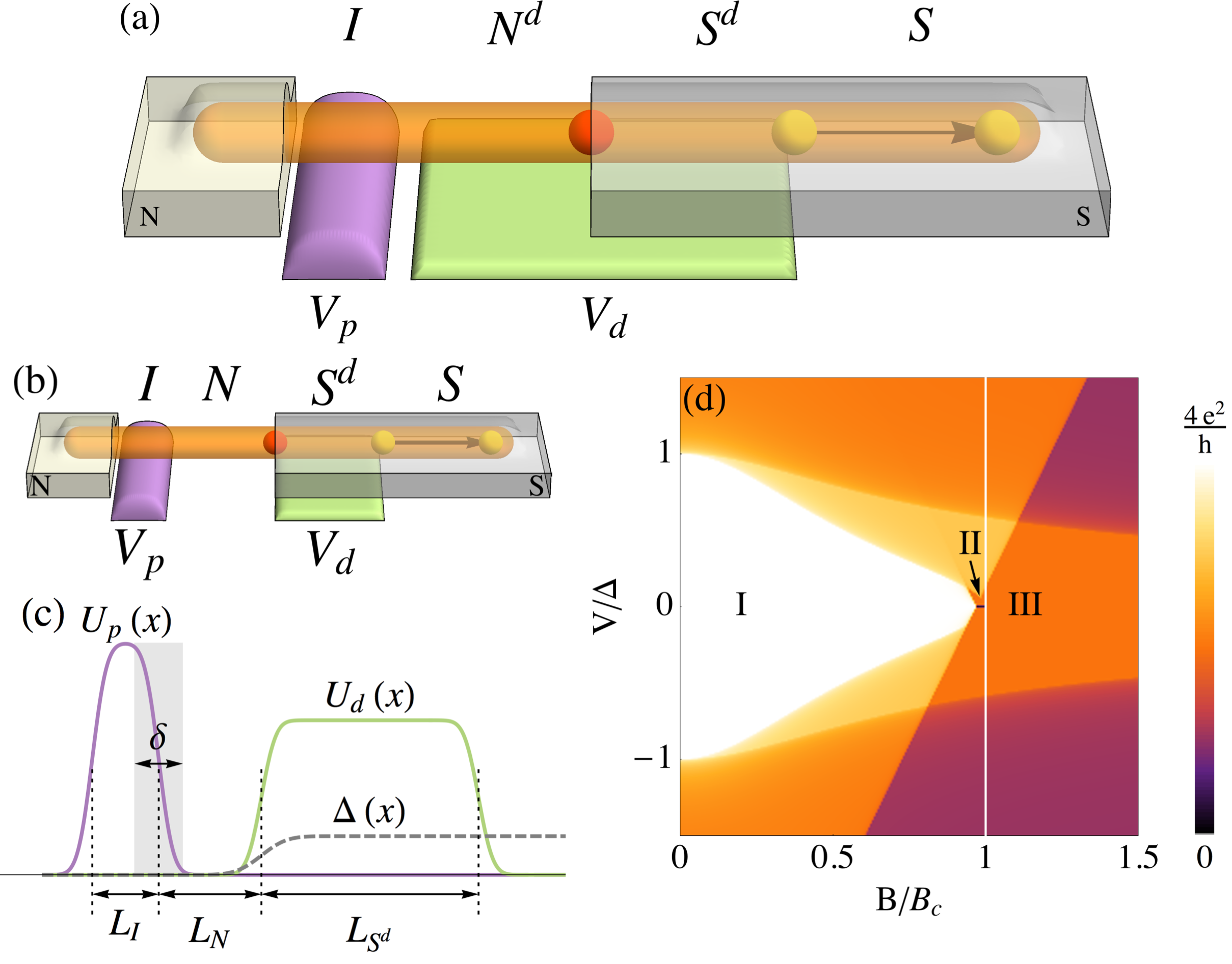
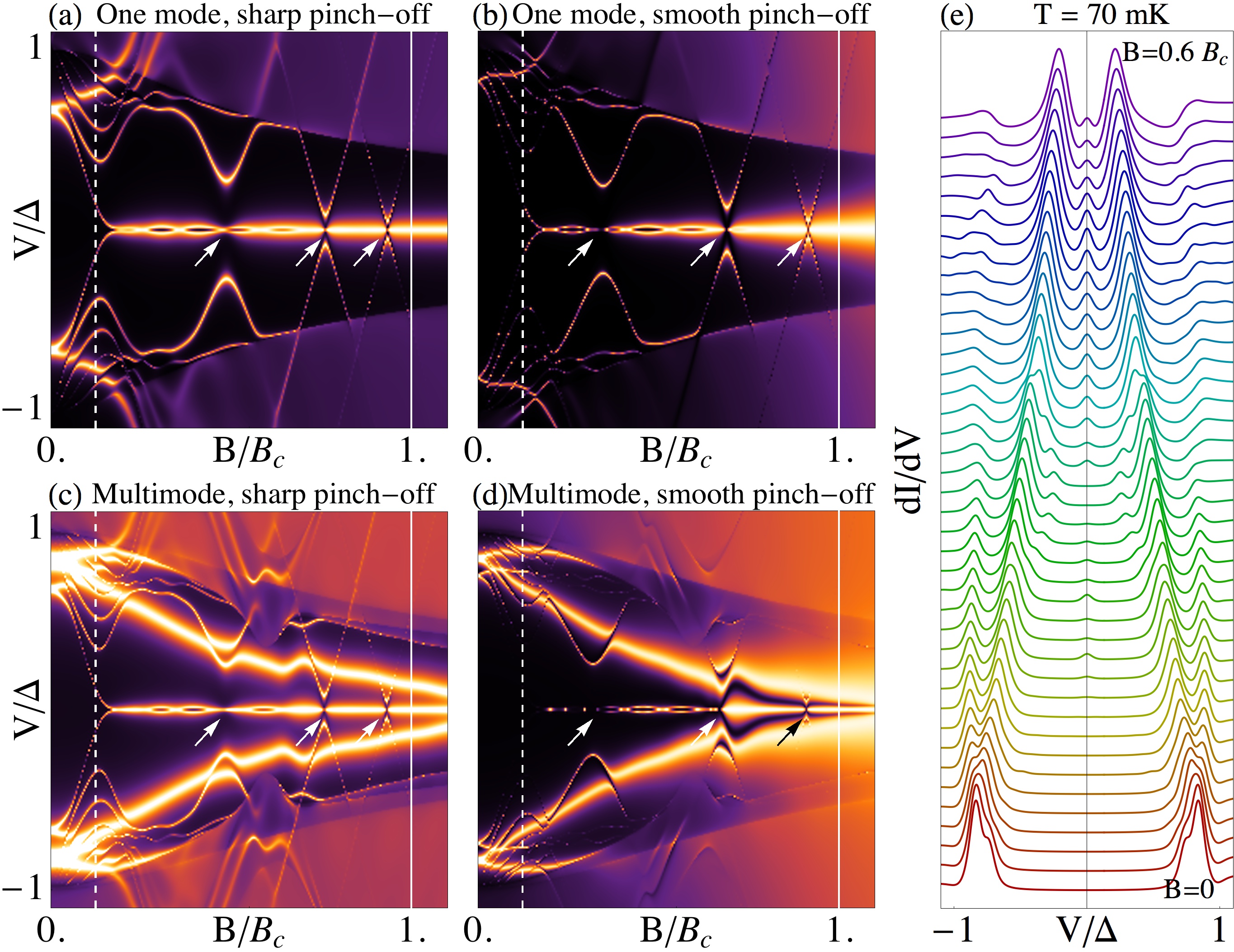
Motivated by this, we present here a detailed study of transport through normal-superconductor (NS) junctions containing topological wires. As in the experiment, the wires are tunnel-coupled to the normal reservoir by a pinch-off gate (to allow for transport spectroscopy using ), and are depleted by an additional gate in order to bring down to accessible fields (since the induced potential lowers the Fermi energy ). The depletion profile, however, is necessarily inhomogeneous, since it cannot extend deep into the superconducting side due to efficient screening, see Fig. 1 and Ref. Mourik et al., 2012. We find that for this class of devices, a number of distinct transport regimes arise as the various sections of the wire transition to different electronic phases. We characterize these regimes and the rich phenomenology that results beyond the simplest picture Sengupta et al. (2001); Bolech and Demler (2007); Law et al. (2009). In particular, we address the question of whether the ZBAs are related to Majorana physics, and confirm that this is indeed the case for long depletion regions. We also analyze the development of ABSs close to zero energy when the pinch-off gate lies at a finite distance from the NS junction. Our main results are summarized in Fig. 4(e) where we demonstrate that the of realistic junctions with inhomogeneous depletion and multisubband filling may not show a distinct closing of the gap and yet exhibit ZBAs of Majorana origin. In most cases, these ZBAs show a residual splitting and may coexist with ABSs, features also observed in Ref. Mourik et al., 2012.
Model.—We first consider a one-dimensional NS junction [see Fig. 1(a)], with a BCS-type Hamiltonian , where
and .
Here is the SO coupling and is the Zeeman splitting (given by , where is an in-plane magnetic field, is the Bohr magneton and is the nanowire g-factor). We assume a position dependent pairing induced by the superconducting electrode such that and . The term is composed of two parts: comes from the pinch-off gate in the normal region at a distance from the NS interface, and models the potential induced by the depletion gate 111This gate has turned out to be crucial for the observation of ZBAs in the Delft experiment.. Gate may extend all the way into the normal side of the NS interface [case , with a depleted length , Fig. 1(a)], or be limited to the end of the superconducting side [case , , Fig. 1(b)]. We will consider the former case first, where we cover different parametric regimes, and then turn to the second one, which is closer to the experimental setup Mourik et al. (2012). Realistic experimental parameters are: is the induced gap that, for an InSb effective mass , corresponds to a length scale . Strong SO coupling, representative of InSb wires Nadj-Perje et al. (2012), is meV nm, with SO length 222These parameters, while probably being a good estimation, are not directly measured in the experiment but rather inferred from different samples in a different geometry. Thus significant changes in cannot be excluded..
Scales.—A localized MBS is formed at the boundary of a trivially gapped and a TS portion of the wire. At a point the wire will be in the TS phase if and
| (1) |
The asymptotic value of the critical field is the proper (bulk) critical field . Apart from , several other Zeeman scales dictate the junction’s transport properties. The first one is the TS critical field in the depleted part of the superconducting wire, , that is smaller than , as is the purpose of the depletion gate. It should be noted, however, that the depleted region has a finite length, which crucially affects Majorana modes for , as discussed later, while the portion is assumed infinite. Secondly, there is the field above which the normal side of the wire becomes a helical liquid (momentum and spin become correlated). In the case (normal side not depleted), this is , which is typically slightly smaller than , but bigger than both and the corresponding helical field in the case, namely . Finally, there is the superconducting gap itself, , whose significance will become clear later. All these scales ( plus in the case, or in the ), control different aspects of the junction’s differential conductance in the - plane.
Differential conductance.—The of a NS junction may be related to the intrinsic conductance at zero temperature by the expression Blonder et al. (1982):
Here, is the number of propagating channels in the normal side at energy , and and are their normal and Andreev reflection matrices. These matrices can be computed in a number of ways. The most flexible is the recursive Nambu Green’s function approach, employed here (for full details, see Sup ).

Before considering the effect of , we show the transport phase diagram [see Fig. 1(c)] in the simple NS transparent limit, i.e. in a regime where the concepts of MBSs and ZBAs do no longer hold. We observe different transport regions in the - plane characterized by an integer , with . Such is the case of Cooper pair transport (region I, ) or single quasiparticle transport (region III, ). The latter is a TS regime, whose topology becomes evident in the despite the fact that the associated Majorana fermion is completely smeared out due to the gapless spectrum for Wimmer et al. (2011); Sau et al. (2012); Gibertini et al. (2012); Chevallier et al. (2012). Between these two regions, the helical regime is characterized by a fully suppressed zero bias conductance (region II, ). These results extend the concept of half-integer conductance quantization Wimmer et al. (2011) beyond linear response.
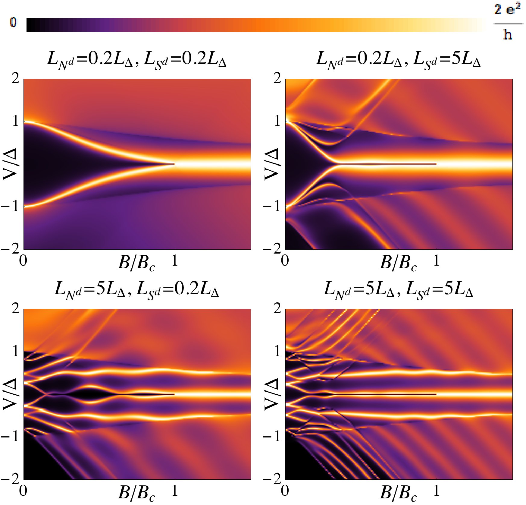
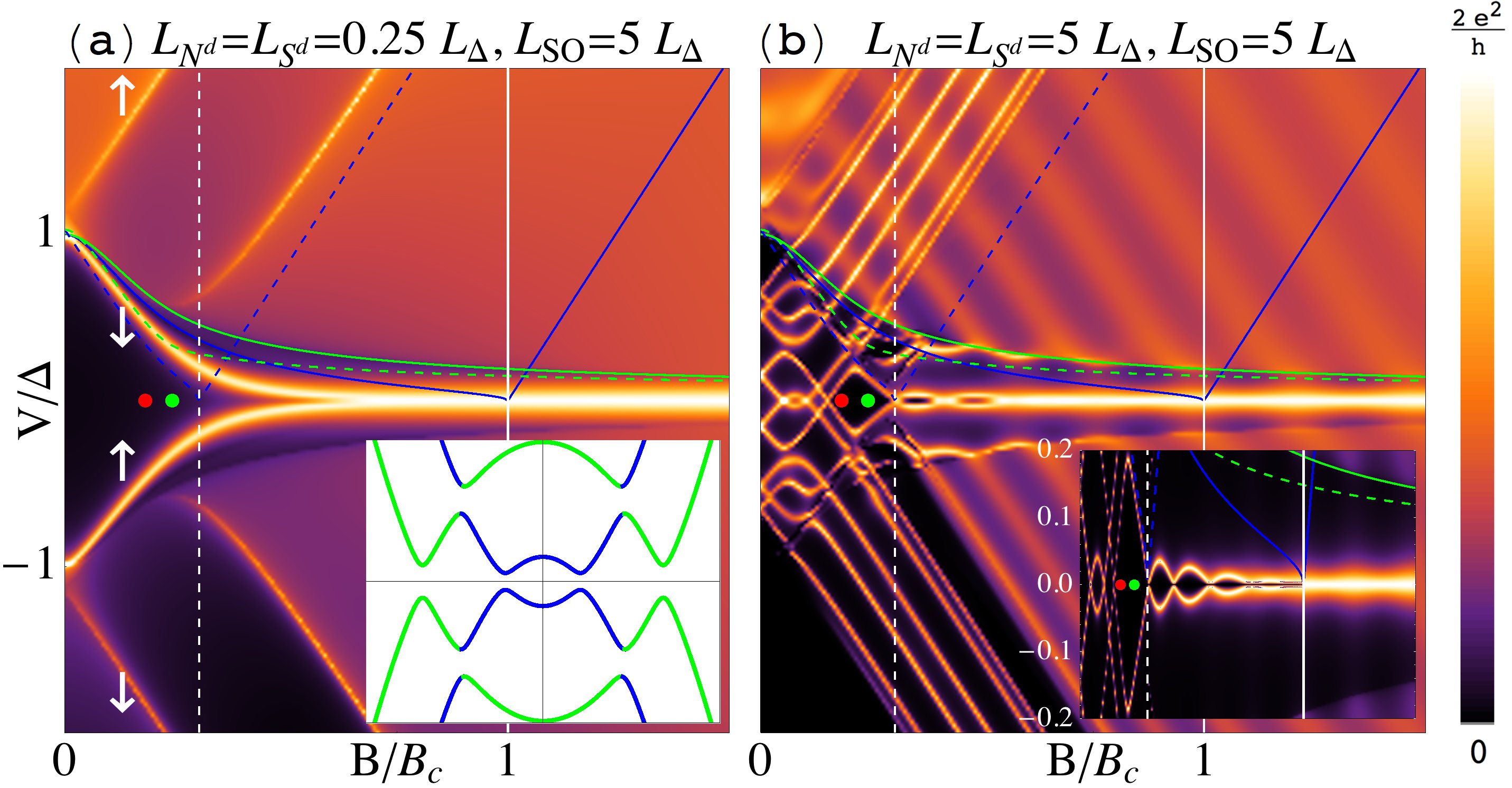
We now consider the junction with the full . Its response (with ) is plotted in Fig. 2. Different panels cover different ratios and . The tunnel barrier is tuned in each case to yield spectroscopic resolution in the transport response. A wide range of behaviours become apparent, that reflect the local density of states (DOS) at the pinch-off gate. The most paradigmatic one is probably the one in the top-left panel. It reflects the closing of the effective superconducting gap (marked by the gap-edge conductance peaks) as increases. The gap-edge DOS peak transforms into a Majorana mode at zero energy for [pictured in Fig. 1(a) as a red sphere]. The gap reopens in the TS phase (see solid blue line in Fig. 3), but the local DOS at the contact is no longer peaked because the spectral weight is transferred to the Majorana mode. Hence, a prototypical three-pronged structure arises in the - plane. However, the relevant phenomenology is by no means exhausted by this. Different scenarios arise at large (Fig. 2, bottom row), with the development of ABSs, or large (right column), with the development of ZBAs below . Further phenomenology is obtained by varying Sup .

Short junction.—We now analyze in more detail the short junction case, (top-left panel in Fig. 2). The scale has little meaning in this case, since any pair of Majorana modes forming at the ends of a short TS wire will strongly hybridize into two conventional states with energies . The effect of increasing is to flatten the gap-edge peak (bright yellow) to lower energies, as shown in Fig. 3(a) (). At these large , spin becomes a good quantum number and the Zeeman field splits the particle and hole bands of the S region into spin up/down subbands (white arrows in Fig. 3). Particle and hole gap edges anticross at zero energy for (green dot), resulting in a minigap (which vanishes for ) with almost flat edges near zero. This structure appears as a (split) ZBA below that is unrelated to Majorana mode formation 333Note that this structure of the remains essentially unchanged in the absence of a depleted region..
Long junction.—Increasing the length of the depleted normal wire gives rise to ABSs in the region that are probed by the tunnel barrier (see bottom row of Fig. 2). Increasing we find these ABSs resonances approaching a degenerate zero energy crossing, see Fig. 3(b). These low energy ABSs, however, cease after the helical transition at (red dot). While the ABSs move up and down in energy for depending on their spin character, as soon as the region becomes helical, all ABSs disperse away from zero energy with increasing , since incoming states do not have spin partners anymore. Beyond the second threshold (vertical dashed white line), the local band gap closes in the region (dashed blue line) and a ZBA builds up, which is caused by Majorana fermion pairs forming in the region of length , also assumed large. The finite , however, produces a residual splitting of the two Majoranas, visible in the ZBA that oscillates with Cheng et al. (2009); San-Jose et al. (2012); Lim et al. (2012); Klinovaja and Loss (2012) as long as . Above the bulk , the rightmost Majorana escapes to (see Fig. 1), where it no longer overlaps with the one at the interface, and the splitting vanishes [see inset of Fig. 3(b)].
junction.—We now turn to the type of setup explored in Ref. Mourik et al., 2012, the case. The crucial difference with the setup is that the ABSs zero energy anticrossings may coexist with Majorana ZBAs in the region, since the region becomes helical after the region becomes topological. When that happens, the zero energy ABSs repel the MBS wavefunction (usually delocalized into the region) back into the region, hence decoupling it from the lead. As a result, the ZBA, as measured by the , is suppressed (see arrows in Fig. 4, where ). In a single mode wire (Fig. 4, top row), this may happen only for , since it requires an interface between a non-helical and a topological 444Therefore, for single mode wires, ABSs cannot coexist with the ZBA near zero energy for . Although this is possible in multimode wires, the ZBA suppression does not occur in such case.. Interestingly, the above behavior agrees with the experimental observation of an intermittent ZBA that disappears and reappears as an ABS anticrosses at zero energy. Constant- sweeps of are also found to closely correlate with the experiment Sup .
A further feature apparent in the experiments is the absence of gap-edge singularities closing just before the formation of the ZBA. Up till now, all potential profiles have been assumed spatially abrupt [decay length in all profiles of Fig. 1(c)]. Imperfect screening, however, will lead to gate-induced potentials that decay slowly along the wire, specially at low electron densities. When a smooth profile is taken into account, the gap-edge peaks are quickly washed out, and the in the tunneling regime is no longer a perfect measure of the local density of states 555This is in stark contrast with local probes such as the tunneling current from a metallic tip into the end of the nanowire, see e.g. Ref. Stanescu et al. (2011). Note moreover that a smooth leaves the largely unaffected, which allows us to bypass a self consistent calculation of the pairing profile.. Unlike for sharp pinch-off barriers, transmission through smooth barriers mostly preserves longitudinal momentum. Since moreover barrier transmission is lower for smaller momenta, the gap-edge resonance closing around zero momentum at is poorly probed by a smooth barrier. Visibility is restored as increases beyond , since then the Zeeman splitting increases the momentum components of all resonances, including the ZBA. Fig. 4(b) shows this effect. Note on the other hand that the gap-edge signal at higher energies is roughly constant in . This corresponds to the large-momentum band edge, not the true gap edge at small momentum. The former band edge shows no sign of the different transitions (the TS transition at in particular), and never closes. Therefore, all zero energy structure appears disconnected from any closing of the gap, as measured by the .
Transport features connected to large momenta should be enhanced in a multisubband systems. The pinch-off condition for tunneling spectroscopy requires a higher barrier in this case, to shut off the additional open modes, which will necessarily contribute with a stronger signal relative to the shallower, lower momentum mode. This is likely the experimental situation in Ref. Mourik et al., 2012, where the observed gap edge signal exceeds the amplitude of the ZBA. In order to confirm this idea, we have performed multisubband transport simulations (see implementation details in Sup ). In Fig. 4(c), (d), we show results corresponding to a fixed defined from the bottom of the topmost subband, which becomes topological at low magnetic fields, while the lower ones remain trivial. The single mode analysis carries over unchanged, albeit with a stronger gap edge and the associated high-momentum structure of the additional modes. Fig. 4(e) shows constant traces of Fig. 4(d) at finite temperature (). Thermal smearing washes out the ZBA splitting, whilst also reducing its height.

Conclusions.—We have identified various transport regimes in depleted NS nanowire junctions with SO coupling and Zeeman field. Depending on the Zeeman field, the wire as a whole may be in any given combination of helical/non-helical and trivial/topological phases for its normal and superconducting portions, respectively. These include a helical depletion () and a topological depletion () phases that arise at fields below those of the proper helical bulk () and topological bulk () regimes. The different phases have distinct sub-gap signatures in transport, particularly if the depleted region is long enough. In this case, ZBAs appear that are caused by the formation of either a single (in the topological bulk phase) or a pair (topologial depletion phase) of Majorana modes in the junction. The latter is characterized by a residual ZBA splitting. In the case of short junctions, Majoranas cannot develop below , although one may still distinguish between the conventional and minigap transport regimes (unrelated to Majorana physics) if is large.
Apart from this general analysis, we have discussed a configuration similar to the one in the experiment of Ref. Mourik et al., 2012. We argue that at least a number of non-trivial features observed in this experiment are consistent with most of our results corresponding to transport through a multi-mode non-helical normal/topological depleted superconductor/trivial bulk superconductor junction, hosting Majorana fermion pairs within the central region [Fig. 4(d), (e)]. While a qualitative correspondence can be traced between our observations and the experiment, a more quantitative agreement is beyond the goal of our study. This is in part due to a considerable number of unknown parameters (precise , screened gate potential profiles, localization and pair-breaking effects in the bulk superconductor Driessen et al. (2012), etc.). Moreover, other features that we find, such as the ZBA splitting oscillations in , have not been observed. Thus, a different physical origin of the measured ZBAs (reflectionless tunneling van Wees et al. (1992), Kondo, etc) cannot be completely excluded. The latter, however, should be accompanied (at least in its most conventional form) with even-odd effects as a function of gate voltages Lee et al. (2012), which are not apparent in Ref. Mourik et al., 2012. Disorder (not considered here) might also be of relevance. However, its precise role on Majorana physics is currently under active investigation Pientka et al. (2012); Bagrets and Altland (2012); Liu et al. (2012).
We are grateful to S. Frolov and L. Kouwenhoven for fruitful discussions. We acknowledge the support of the CSIC JAE-Doc program and the Spanish Ministry of Science and Innovation through Grant No. FIS2008-00124/FIS (P.S.-J), FIS2009-08744 (E.P. and R.A.). This research was supported in part by the National Science Foundation under Grant No. NSF PHY05-51164.
References
- Volovik (1999) G. Volovik, JETP Lett. 70, 609 (1999).
- Read and Green (2000) N. Read and D. Green, Phys. Rev. B 61, 10267 (2000).
- Fu and Kane (2008) L. Fu and C. L. Kane, Phys. Rev. Lett. 100, 096407 (2008).
- Sato et al. (2009) M. Sato, Y. Takahashi, and S. Fujimoto, Phys. Rev. Lett. 103, 020401 (2009).
- Sau et al. (2010a) J. D. Sau, R. M. Lutchyn, S. Tewari, and S. Das Sarma, Phys. Rev. Lett. 104, 040502 (2010a).
- Alicea (2010) J. Alicea, Phys. Rev. B 81, 125318 (2010).
- Lutchyn et al. (2010) R. M. Lutchyn, J. D. Sau, and S. Das Sarma, Phys. Rev. Lett. 105, 077001 (2010).
- Oreg et al. (2010) Y. Oreg, G. Refael, and F. von Oppen, Phys. Rev. Lett. 105, 177002 (2010).
- Beenakker (2011) C. W. J. Beenakker, arXiv:1112.1950v1 (2011).
- Alicea (2012) J. Alicea, Rep. Prog. Phys. 75, 076501 (2012).
- Mourik et al. (2012) V. Mourik, K. Zuo, S. M. Frolov, S. R. Plissard, E. P. A. M. Bakkers, and L. P. Kouwenhoven, Science 336, 1003 (2012).
- Deng et al. (2012) M. T. Deng, C. L. Yu, G. Y. Huang, M. Larsson, P. Caroff, and H. Q. Xu, arXiv:1204.4130v1 (2012).
- Das et al. (2012) A. Das, Y. Ronen, Y. Most, Y. Oreg, M. Heiblum, and H. Shtrikman, arXiv:1205.7073v1 (2012).
- Sengupta et al. (2001) K. Sengupta, I. Zutik, H.-J. Kwon, V. M. Yakovenko, and S. Das Sarma, Phys. Rev. B 63, 144531 (2001).
- Bolech and Demler (2007) C. J. Bolech and E. Demler, Phys. Rev. Lett. 98, 237002 (2007).
- Law et al. (2009) K. T. Law, P. A. Lee, and T. K. Ng, Phys. Rev. Lett. 103, 237001 (2009).
- Sau et al. (2010b) J. D. Sau, S. Tewari, R. M. Lutchyn, T. D. Stanescu, and S. Das Sarma, Phys. Rev. B 82, 214509 (2010b).
- Stanescu et al. (2011) T. D. Stanescu, R. M. Lutchyn, and S. Das Sarma, Phys. Rev. B 84, 144522 (2011).
- Note (1) This gate has turned out to be crucial for the observation of ZBAs in the Delft experiment.
- Nadj-Perje et al. (2012) S. Nadj-Perje, V. S. Pribiag, J. W. G. van den Berg, K. Zuo, S. R. Plissard, E. P. A. M. Bakkers, S. M. Frolov, and L. P. Kouwenhoven, Phys. Rev. Lett. 108, 166801 (2012).
- Note (2) These parameters, while probably being a good estimation, are not directly measured in the experiment but rather inferred from different samples in a different geometry. Thus significant changes in cannot be excluded.
- Blonder et al. (1982) G. E. Blonder, M. Tinkham, and T. M. Klapwijk, Phys. Rev. B 25, 4515 (1982).
- (23) See Appendix for a description of the recursive Green’s function algorithm for computing transport, including finite width and finite temperature. Also included is an extensive parametric study of differential conductance for varying geometric parameters and spin-orbit lengths, as well as differential conductance maps as a function of bias and depletion gate voltage.
- Wimmer et al. (2011) M. Wimmer, A. R. Akhmerov, J. P. Dahlhaus, and C. W. J. Beenakker, New J. Phys. 13, 053016 (2011).
- Sau et al. (2012) J. D. Sau, C. H. Lin, H.-Y. Hui, and S. Das Sarma, Phys. Rev. Lett. 108, 067001 (2012).
- Gibertini et al. (2012) M. Gibertini, F. Taddei, M. Polini, and R. Fazio, Phys. Rev. B 85, 144525 (2012).
- Chevallier et al. (2012) D. Chevallier, D. Sticlet, P. Simon, and C. Bena, Phys. Rev. B 85, 235307 (2012).
- Note (3) Note that this structure of the remains essentially unchanged in the absence of a depleted region.
- Cheng et al. (2009) M. Cheng, R. M. Lutchyn, V. Galitski, and S. Das Sarma, Phys. Rev. Lett. 103, 107001 (2009).
- San-Jose et al. (2012) P. San-Jose, E. Prada, and R. Aguado, Phys. Rev. Lett. 108, 257001 (2012).
- Lim et al. (2012) J. S. Lim, L. Serra, R. Lopez, and R. Aguado, Phys. Rev. B 86, 121103 (2012).
- Klinovaja and Loss (2012) J. Klinovaja and D. Loss, Phys. Rev. B 86, 085408 (2012).
- Note (4) Therefore, for single mode wires, ABSs cannot coexist with the ZBA near zero energy for . Although this is possible in multimode wires, the ZBA suppression does not occur in such case.
- Note (5) This is in stark contrast with local probes such as the tunneling current from a metallic tip into the end of the nanowire, see e.g. Ref. Stanescu et al. (2011). Note moreover that a smooth leaves the largely unaffected, which allows us to bypass a self consistent calculation of the pairing profile.
- Driessen et al. (2012) E. F. C. Driessen, P. C. J. J. Coumou, R. R. Tromp, P. J. de Visser, and T. M. Klapwijk, Phys. Rev. Lett. 109, 107003 (2012).
- van Wees et al. (1992) B. J. van Wees, P. de Vries, P. Magnée, and T. M. Klapwijk, Phys. Rev. Lett. 69, 510 (1992).
- Lee et al. (2012) E. J. H. Lee, X. Jiang, R. Aguado, G. Katsaros, C. M. Lieber, and S. De Franceschi, Phys. Rev. Lett. 109, 186802 (2012).
- Pientka et al. (2012) F. Pientka, G. Kells, A. Romito, P. W. Brouwer, and F. von Oppen, arXiv:1206.0723v1 (2012).
- Bagrets and Altland (2012) D. Bagrets and A. Altland, arXiv:1206.0434v1 (2012).
- Liu et al. (2012) J. Liu, A. C. Potter, K. Law, and P. A. Lee, arXiv:1206.1276v1 (2012).
See pages 1,,2,3,4,5 of prada-sanjose-aguado-SI