Graphene-based voltage-tunable coherent terahertz emitter
Abstract
A portion of the electromagnetic wave spectrum between and terahertz (THz) suffers from the lack of powerful, effective, easy-to-use and inexpensive emitters, detectors and mixers. We propose a multilayer graphene – boron-nitride heterostructure which is able to emit radiation in the frequency range THz with the power density up to W/cm2 at room temperature. The proposed device is extremely thin, light, flexible, almost invisible and may completely cover the needs of science and technology in the sources of terahertz radiation.
Index Terms:
Terahertz radiation, emitters, graphene, boron nitride.If a fast electron moves in a periodic potential with the average velocity , its momentum , as well as velocity , oscillates in time with the frequency
| (1) |
Since electrons are charged particles, such a motion is accompanied by an electromagnetic radiation with the frequency (1), Ref. [1]. This physical principle is used in backward-wave oscillators and free-electron lasers, where the potential is produced by periodic in space electric or magnetic fields. The frequency of radiation can be tuned in these devices by varying the accelerating voltage which determines the electron velocity .
It was a long dream of scientists and engineers to create a compact solid-state emitter operating on the same physical principle. For example, [2, 3, 4, 5] such an idea could be realized in semiconductor structures with a two-dimensional (2D) electron gas: placing a metallic grating in the vicinity of the 2D conducting layer and driving electrons across the grating stripes it seemed to be possible to force all electrons to emit electromagnetic waves at the frequency (1). However, instead of the strong coherent emission at the frequency (1) a weak thermal radiation at the frequency of two-dimensional plasmons
| (2) |
was observed [2, 3, 4, 5]; here , and are the charge, the effective mass and the surface density of 2D electrons and the dielectric constant of surrounding medium.
The reason of this failure was explained in Ref. [6]. It was shown that the single-particle formula (1) is valid only at , i.e. if the density of electrons is low or the drift velocity is sufficiently high. This condition is easily satisfied in vacuum devices and free-electron lasers. In a dense solid-state plasma one should take into account electron-electron interaction effects. Then one finds [6] that the strong coherent radiation is observed at the frequency
| (3) |
only if the velocity exceeds a threshold value
| (4) |
for details see [6]. Otherwise, at , electrons emit at the plasma frequency (2), just due to the heating of the system (the thermal radiation).
The condition (4) is of crucial importance for successful device operation. It shows that the surface electron density should be low and the drift velocity should be large. This condition is very difficult, if possible at all, to fulfil in semiconductor structures. For example, in a GaAs quantum well with , , cm-2 and m the threshold velocity (4) is about cm/s which is more than 4 times larger than the Fermi velocity at the same density.
In graphene, a recently discovered [7, 8, 9] only one-atom-thin, truly two-dimensional carbon material, the spectrum of electrons is linear,
| (5) |
with a very large, as compared to semiconductors, Fermi velocity cm/s. This makes graphene an ideal candidate for the realization of the old idea to create a voltage tunable solid-state terahertz emitter, see illustration in Figure 1.
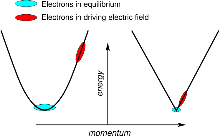
However, an attempt to directly apply the above described ideas to graphene faces two difficulties. First, in graphene oscillations of the momentum do not lead to oscillations of the velocity and, hence, of the current, since the velocity is not proportional to the momentum. Second, the condition restricts the required electron density by the values of order of cm-2. It is known, however, that due to internal inhomogeneities (electron-hole puddles [10]) the average density of electrons in a graphene sheet typically exceeds cm-2 even at the Dirac point.
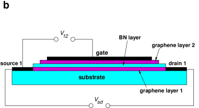
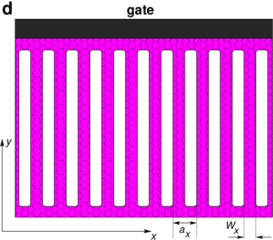
The both difficulties can be overcome by using, instead of continuous graphene layers, an array of narrow stripes of graphene. This leads to the following basic design of the emitter [11], Figure 2. The first (active) graphene layer lies on a substrate made out of a dielectric material, e.g. SiO2 or hexagonal boron nitride (-BN), Figures 2a. This layer consists of an array of stripes with the width and the period and has two metallic contacts “source 1” and “drain 1”, Figure 2c. Above the first graphene sheet lies a thin dielectric layer, made out of a few monolayers of -BN. A second graphene layer, Figure 2d, has the shape of a grating with the stripe width and the period , oriented perpendicular to the stripes of the first layer and covers the whole structure. It has a metallic “gate” contact, Figure 2d. The side view of the whole structure is shown in Figure 2b.


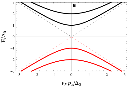
Due to the finite width of graphene stripes in the first layer, the -component of the momentum is quantised, , and a gap is opened up in the graphene spectrum,
| (6) |
Figure 3a. The value of the gap,
| (7) |
is controlled by the stripe width and can be as large as meV ( K) if m. The linear density of electrons and holes per unit length then reads
| (8) |
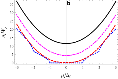
where is the chemical potential, is the temperature and are spin and valley degeneracies. As seen from Figure 3b, the total linear charge density is about at room temperature. At m this gives cm-1. If to choose the period of the structure in the first layer bigger than m, the average surface density will be smaller than cm-2. Thus, by choosing a sufficiently large ratio one can always satisfy the threshold condition (4). This can also be seen from the expression
| (9) |
which should be smaller than unity (Eq. (9) follows from (4) if to replace by ). The first factor here is of order unity. The second factor depends on the temperature, Figure 3b, and is about 10 at room and about 1 at liquid nitrogen temperature. The last factor can be made as small as desired by the corresponding choice of geometrical parameters of the structure.
In the operation mode, Figure 2b, a large dc voltage is applied between the source and drain contacts of the first layer and a small dc (gate) voltage – between the first and the second graphene layer. The source–drain voltage causes a dc current in the first-layer stripes flowing in the -direction. The corresponding drift velocity should lie in the window . If the drift velocity is about cm/s and the grating period m, the fundamental frequency of the emitter will be about 3 THz. Dependent on the parameters this frequency can be red- or blue-shifted.
Let us estimate the power of the emitted radiation. Under the action of the dc source–drain voltage electrons move with the constant drift velocity . A small gate voltage applied between the first and the second graphene layers results in the periodic time-dependent modulation of the velocity, . The modulation amplitude is controlled by the gate voltage and can be varied between 0 and . Assume that we have a 70%-modulation of the drift velocity, i.e. cm/s. Then the amplitude of the ac electric current density is , the electric and magnetic fields of the emitted wave (calculated from Maxwell equations) are and the intensity of the emitted radiation (the Poynting vector) . At the electron density cm-2 this gives a very large radiation power of
| (10) |
Estimating the Joule’s heating power as , where is the minimal conductivity of graphene [8], we get
| (11) |
i.e. the efficiency of the emitter is about 1%. If the structure lies on a SiO2 or BN 1 mm-thick substrate and the opposite side of the substrate is maintained at room temperature, the increase of temperature of the structure at W/cm2 does not exceed 10–20 K, due to the very large surface-to-volume ratio in the two-dimensional graphene and to the high thermal conductivity of the substrate.
The proposed device may emit radiation not only at the fundamental frequency (1) but also at its harmonics. In the above discussion we have assumed that the periodic potential produced by the voltage between the two graphene layers has a simple sinusoidal form . This is a good approximation for the case when the distance between the 2D electron layer and the grating is comparable with the grating period. In the proposed graphene–BN–graphene device the thickness of the dielectric BN layer can be as small as a few nanometers while the realistic value of the grating period is m. The ratio is therefore much smaller than unity and the potential has a step-like form, see Inset in Figure 4b. The higher spatial harmonics will then lead to higher frequency harmonics in the emission spectrum. To show this quantitatively, we solve the Newton equations of motion for an electron in the graphene stripe
| (12) | |||||
| (13) |
where is the dc electric field caused by the source-drain voltage, is the distance between the source and the drain and is a phenomenological parameter describing the “friction force” due to the scattering. For the periodic potential we use a simple model expression
| (14) |
where is the potential amplitude and the parameter determines the steepness of , Figure 4b: if , the periodic potential is smooth and close to a single-harmonic sinusoidal form; if , it has a step-like form and contains many spatial Fourier harmonics. Equations (12)–(13) are written for an electron of the first subband ; evidently, taking into account the higher electron and all hole subbands will not significantly change the results. In these equations we also ignore the plasma effects since we assume that the electron density is sufficiently low, the parameter , Eq. (9), is small and the threshold condition (4) is satisfied, as has been discussed above. There are two sources of nonlinearity in equations (12)–(13): the non-sinusoidal periodic potential and graphene-specific nonlinear velocity-momentum relation.

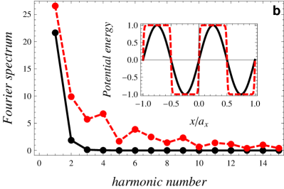
Figure 4 shows results of the numerical solution of equations (12)–(13) for parameters , and . If K meV the first two numbers correspond to meV and V/cm for the grating period m respectively. The last number means that the mean free path is of order of the grating period, i.e. m for the same values of (notice that the parameter is not very crucial: the device will work both at and at ). It is quite possible to realise all these requirements in experiments. Figures 4a and 4b show the time dependence of the velocity and its Fourier spectra respectively; the black (solid) and the red (dashed) curves correspond to the small () and large () values of the steepness parameter . One sees that at the current has an almost sinusoidal form with the dominating first and substantially weaker second frequency harmonics. The average drift velocity for the chosen parameters is which corresponds to the fundamental frequency (1) THz for m. At the time dependence of the current is strongly non-monochromatic with quite large second, third, fourth and even sixth frequency harmonics. The average drift velocity for the chosen parameters is with the resulting fundamental frequency . This corresponds, for the same values of the grating period m, to the first harmonic THz, second harmonic THz, fourth harmonic THz and so on. As seen from Figure 4(b) even the ninth harmonic ( is up to 27 THz) has the amplitude only one order of magnitude smaller than the first one. The emitted radiation is linearly polarised in the direction of the dc current (-direction).
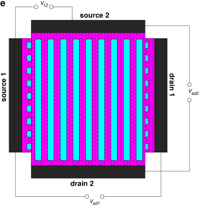
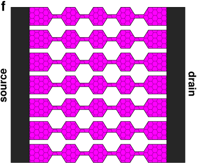
So far we have discussed the traditional field-effect-transistor-type design with the top graphene layer having only one (gate) contact, Figure 2d. Alternatively, the top layer may have two metallic contacts, “source 2” and “drain 2”, which gives the opportunity to drive a dc current in the second layer too, Figure 2e. Then the system becomes symmetric, with the second (first) layer serving as the grating coupler for the first (second) layer and the opportunity to emit radiation with both - and -polarization independently controlled by the source-drain voltages and . Another possible embodiment employing a single graphene layer is shown in Figure 2f. The periodic potential is produced in this case by the alternating stripe width . An advantage of this design is that it employs only one graphene layer. In this case, however, the mean free path should exceed the grating period .
In addition to the ability to work as an emitter, the proposed device may also operate as a new type of a field-effect-transistor (amplifier) combined with a plane radiating antenna. Indeed, the intensity of the emitted radiation is determined by the amplitude of the ac electric current . This amplitude depends, in its turn, on the voltage between the first and second graphene layers: if , the current flowing from the source to the drain does not depend on time and no radiation is emitted; if , the current gets modulated and the device emits an electromagnetic signal. The radiation intensity can be very large ( kilowatts from square meter, Eq. (10)) at the few-millivolt input signal (see estimates above). The proposed device thus amplifies an input signal and sends it directly to the surrounding space within the same physical process.
The single-layer graphene absorbs only 2.3% of visible light [12]. The -BN layer is a dielectric with a large band gap and is also transparent. The proposed powerful terahertz devices will therefore be very thin, light and practically invisible. Furthermore, such few-nm thick devices can be bent up focusing radiation and producing a huge concentration of THz power in a very small spatial volume.
To summarise, we have proposed a new type of few-atomic-layers thin, light, bendable, almost invisible and voltage tunable graphene based device which is able to produce a powerful electromagnetic radiation in a broad range of terahertz frequencies. This device may cause a revolution in the terahertz science and technology and will have a lot of applications in many different areas.
Acknowledgment
The author would like to thank Ulrich Eckern and Roland Grenz for interest to this work and Geoffrey Nash, Fabrizio Castellano and Jerome Faist for useful discussions. This work was supported by Deutsche Forschungsgemeinschaft.
References
- [1] S. J. Smith and E. M. Purcell, “Visible light from localized surface charges moving across a grating,” Phys. Rev., vol. 92, p. 1069, 1953.
- [2] D. C. Tsui, E. Gornik, and R. A. Logan, “Far infrared emission from plasma oscillations of Si inversion layers,” Solid State Commun., vol. 35, pp. 875–877, 1980.
- [3] R. A. Höpfel, E. Vass, and E. Gornik, “Thermal excitation of two-dimensional plasma oscillations,” Phys. Rev. Lett., vol. 49, pp. 1667–1671, 1982.
- [4] N. Okisu, Y. Sambe, and T. Kobayashi, “Far-infrared emission from two-dimensional plasmons in AlGaAs/GaAs heterointerfaces,” Appl. Phys. Lett., vol. 48, pp. 776–778, 1986.
- [5] K. Hirakawa, K. Yamanaka, M. Grayson, and D. C. Tsui, “Far-infrared emission spectroscopy of hot two-dimensional plasmons in Al0.3Ga0.7As/GaAs heterojunctions,” Appl. Phys. Lett., vol. 67, pp. 2326–2328, 1995.
- [6] S. A. Mikhailov, “Plasma instability and amplification of electromagnetic waves in low-dimensional electron systems,” Phys. Rev. B, vol. 58, pp. 1517–1532, 1998.
- [7] K. S. Novoselov, A. K. Geim, S. V. Morozov, D. Jiang, Y. Zhang, S. V. Dubonos, I. V. Grigorieva, and A. A. Firsov, “Electric field effect in atomically thin carbon films,” Science, vol. 306, pp. 666–669, 2004.
- [8] K. S. Novoselov, A. K. Geim, S. V. Morozov, D. Jiang, M. I. Katsnelson, I. V. Grigorieva, S. V. Dubonos, and A. A. Firsov, “Two-dimensional gas of massless Dirac fermions in graphene,” Nature, vol. 438, pp. 197–200, 2005.
- [9] Y. Zhang, Y.-W. Tan, H. L. Stormer, and P. Kim, “Experimental observation of the quantum Hall effect and Berry’s phase in graphene,” Nature, vol. 438, pp. 201–204, 2005.
- [10] J. Martin, N. Akerman, G. Ulbricht, T. Lohmann, J. H. Smet, K. von Klitzing, and A. Yacoby, “Observation of electron-hole puddles in graphene using a scanning single-electron transistor,” Nature Physics, vol. 4, pp. 144–148, 2008.
- [11] S. A. Mikhailov, “European patent (pending),” December 2011.
- [12] R. R. Nair, P. Blake, A. N. Grigorenko, K. S. Novoselov, T. J. Booth, T. Stauber, N. M. R. Peres, and A. K. Geim, “Fine structure constant defines visual transparency of graphene,” Science, vol. 320, pp. 1308–1308, 2008.