The influence of the buffer layer architecture on transport properties for BaFe1.8Co0.2As2 films on technical substrates.
Abstract
A low and almost temperature independent resistance in the normal state and an anomalous peak effect within the normal-superconducting transition have been observed in BaFe1.8Co0.2As2/Fe bilayers, prepared on IBAD-MgO/Y2O3 buffered technical substrates. A resistor network array sufficiently reproduces this effect, assuming an increase of the electrical conductance between tape and film with decreasing buffer layer thickness. Based on this model we evaluated the influence of this effect on the critical current density and successfully reconstructed the superconducting transition of the bilayer.
The development of the coated conductors technology proved high temperature superconductors to become commercially attractive in high current applications. Basically two approaches have been focused on: rolling assisted biaxially textured substrates (RABiTs) and ion beam assisted deposition (IBAD) of textured buffer layers on polycrystalline metal tapesGoy04 ; Iij04 . Recently, the growth of Fe-based superconductors such as BaFe2-xCoxAs2 (Ba-122) and FeSe0.5Te0.5 on IBAD-MgO/Y2O3/Hastelloy has been demonstrated. Their high critical current densities at liquid He temperature as well as their high upper critical magnetic fields make them suitable for high-current applications Iid11 ; Kat11 ; Li11 . In this letter we investigate the normal-superconducting transition for Ba-122 prepared on IBAD-MgO/Y2O3 buffered Hastelloy tapes with varying Y2O3 thickness. We will point out that the observed peak in the resistive transition can be modeled and quantitatively explained using a simple resistor network attributing good electrical conductance between Ba-122/Fe bilayer and tape in the case of a thinner buffer stack. Finally, we show that this model enables an accurate evaluation of important technical properties, such as critical temperature () and critical current density ().
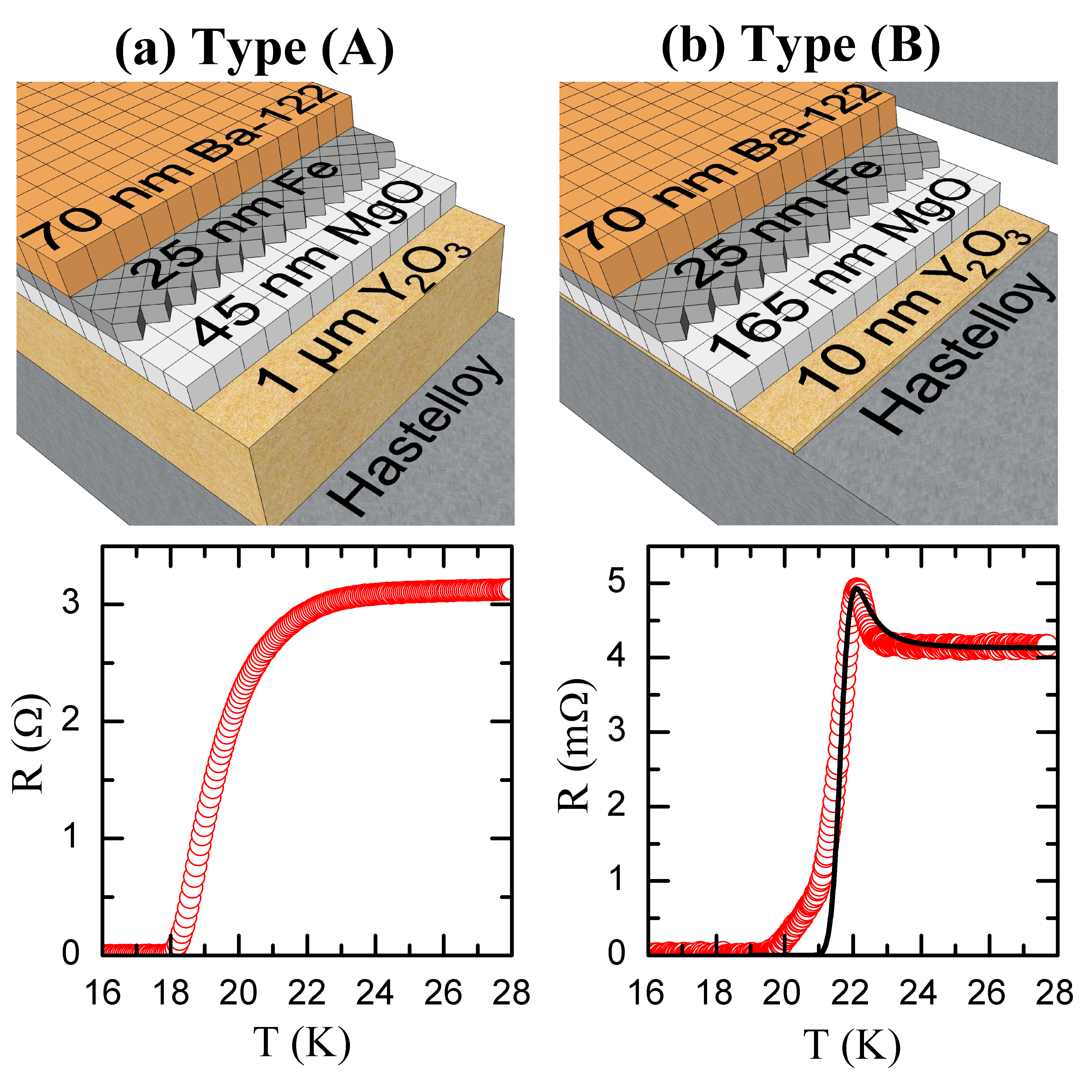
For comparison we used two different buffer architectures on polycrystalline C-276 tape (Hastelloy). Tape (A) was planarized by solution deposition planarization (SDP) process using multiple chemical solution coatings of Y2O3 with a total thickness of approximately 1 m. To obtain a biaxially textured buffer a MgO seed layer was prepared by IBAD at room temperature covered with homoepitaxial MgO of about 40 nm at 600 °C by electron beam sublimation She11 . Tape (B) utilizes electro-polished Hastelloy, covered by a 10 nm thick amorphous electron-beam-deposited Y2O3 layer. On the 5 nm IBAD-MgO template 160 nm homoepitaxial MgO was deposited with electron beam sublimationMat09 . The thicker Y2O3 buffer is commonly used to prevent oxide superconductors from deteriorating the superconducting properties due to a reduced diffusion of transition metal ions from the tape into the film Mat10 .

For both tapes, (A) and (B), a Ba-122/Fe bilayer was prepared in a pulsed laser deposition (PLD) setup with a base pressure of 10-9 mbar applying in-situ reflection high energy diffraction (RHEED) to monitor the film evolution Iid11 . 70 nm Ba-122 were deposited on 25 nm Fe, which was shown to be beneficial for the textured growth of Ba-122 The10 . After cooling to room temperature the sample was covered with Au without breaking the vacuum to ensure low contact resistance. X-ray diffraction proves the phase formation of Ba-122, whereas pole figure measurements as well as RHEED verify the epitaxial relationship (001)[100]Ba-122 (001)[110]Fe (001)[100]MgO Iid11 . Transport measurements were performed in four-probe geometry using a Physical Property Measurement System (PPMS; Quantum Design). For the determination of tracks were prepared by ion etching with 1 mm width and 1 mm length.
The normal-superconducting transition of Ba-122 films on the tapes (A), displayed in fig.1(a), have a typical shape comparable to films prepared on single crystals Iid10_2 . In contrast, films prepared on substrate type (B) (thin Y2O3 layer) exhibit a remarkable shape of the transition as illustrated in fig.1(b). The resistance in the normal state is three orders of magnitude smaller with almost no temperature dependence. Close above the superconducting transition the resistivity peaks, followed by a sharp drop to zero. These features are common for films prepared on tapes (B) independently of and preparation conditions. Hence, they are a consequence of the tape architecture. Peak effects in the temperature dependent resistivity have also been observed in underdoped BaFe2-xCoxAs2. However, they are accompanied by a reduced and can not explain our observations Ni08 .

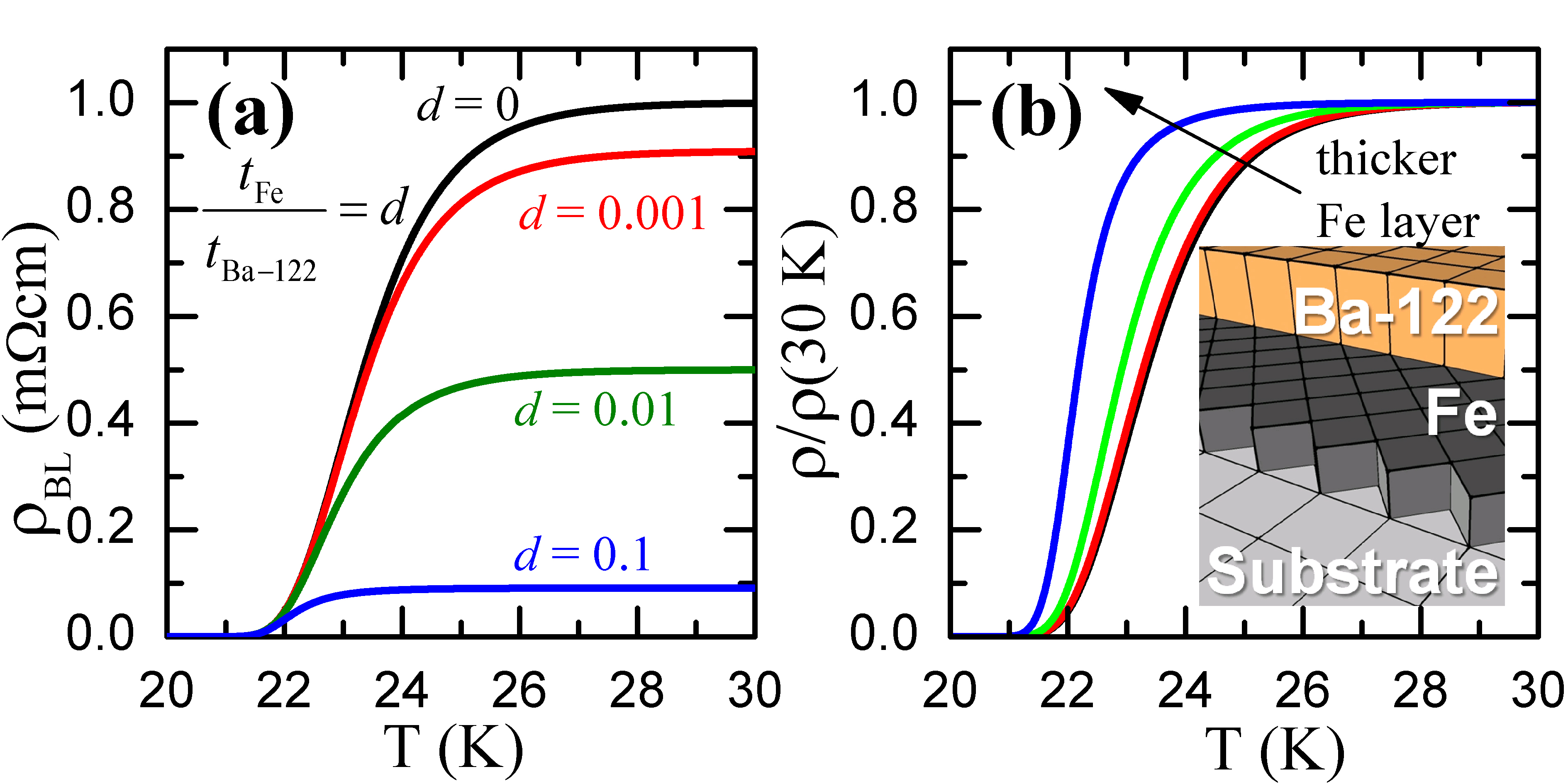
The reduction of the normal state resistivity of Ba-122/Fe bilayers () with increasing ratio in thickness between Fe () and Ba-122 () was reported previously Iid10_2 . This effect is demonstrated in fig.2(a), assuming a simple parallel circuit representing the resistivity of the Fe () and the Ba-122 layer (), where . The superconducting transition can be described as:
| (1) |
where mcm corresponds to the Ba-122 resistivity in the normal state and was taken from single crystal data Ni08 . The parameter determines the width of the transition and is set to 25 in our case. The resistivity of pure Fe amounts to 0.01 cm at 20 K and increases about 1 cm per 1 at% Co diffusion Landolt . Due to the unknown Co content of the Fe layer its resistivity was estimated to a upper limit of 10 cm. In general, both, and , are temperature dependent functions, but were set constant in first-order approximation.
The thickness of Fe in Ba-122/Fe bilayers has to exceed the threshold for a closed layer, which is between 4 nm and 15 nm, to ensure a complete coverage film for the epitaxial growth of Ba-122 Iid10_2 . Hence, the resulting thickness ratios () are in the order of 0.1 including an important consequence, displayed in figure 2(b): The width of the superconducting transition of the Ba-122/Fe bilayer decreases with increasing Fe layer thickness. Therefore, its transition temperature is not identical to the single Ba-122 layer using the same criterion. It has to be considered that the evaluated from transport measurements of bilayers differs from the values of the bare superconducting compound, which is especially important regarding application of multilayered film architectures.
The description of the resistive transition for tape (B) needs additional considerations to be taken into account. A significant consequence of the varying buffer thickness is the influence on the electrical barrier properties between superconductor and tape. In the case of tape (B) an electrical connection can arise from defects in tape which give rise to pinholes in the buffer. This presumption is supported by the fact that in contrast to the used electro-polished tape comparable buffer stacks on smoother mechanically polished tapes are completely insulating. Additionally diffusion of metal ions from tape and Fe buffer can increase the conductivity of the MgO buffer. A thick Y2O3 buffer suppresses the diffusion and overgrows the defects. In the following we will show that a change of the oxide buffer layer resistance by two orders of magnitude gives rise to the observed resistance peak at for tape (B).
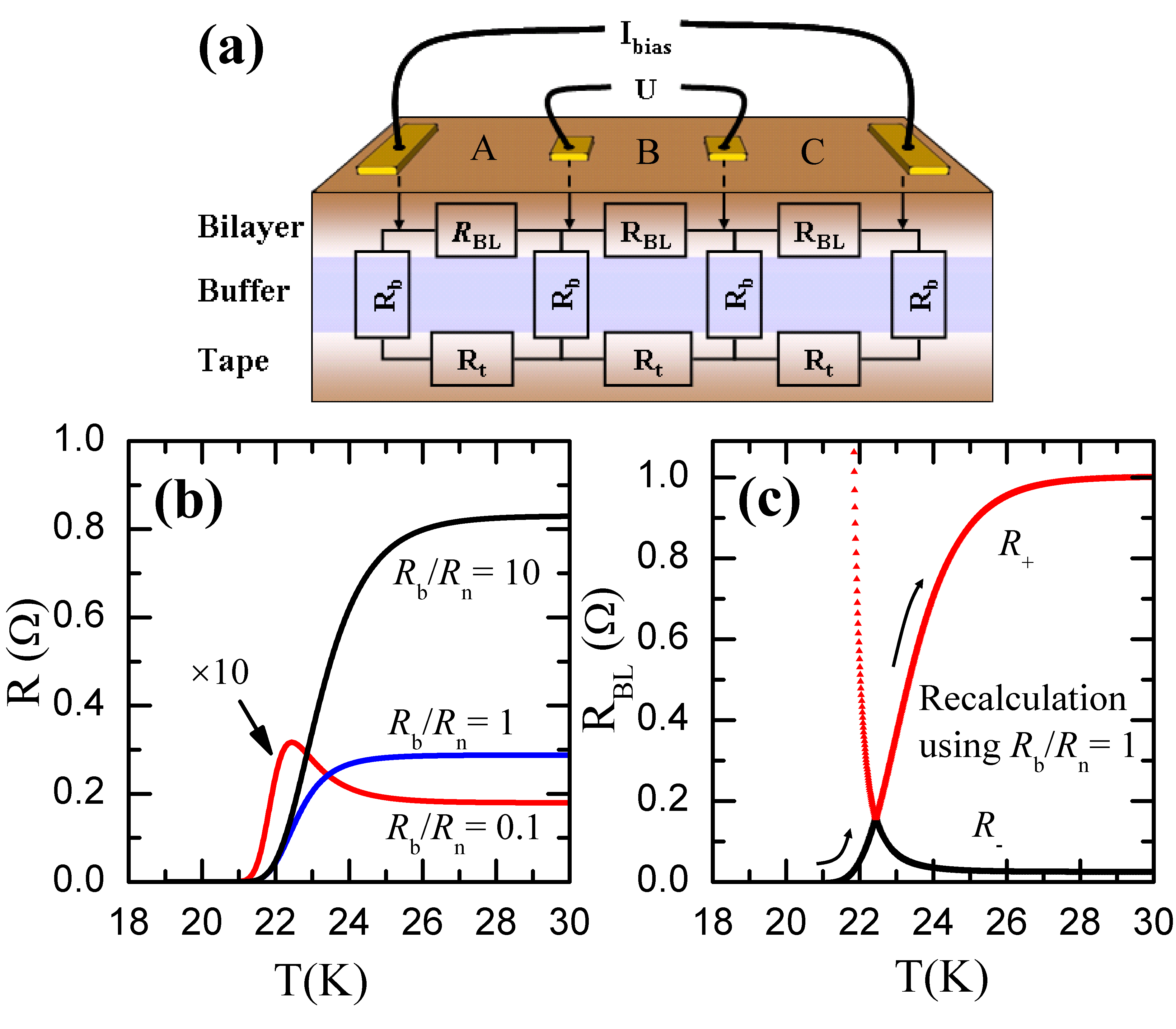
Above the current is shunted by the tape, if the Ba-122 film and metal tape are electrically good connected, as the resistivity of Ba-122 is one order of magnitude larger compared to Hastelloy Ni08 ; Lu08 . Therefore, most of the bias current flows through the tape, which gives only a small voltage drop between the voltage leads. Within the superconducting transition the fraction of current through the film increases with decreasing resistance of the Ba-122 film resulting in an increasing voltage drop between the voltage leads, which finally reaches zero when the film becomes fully superconducting. Taking this into account, we split the sample geometry into three segments, separated by the voltage contacts, which is schematically illustrated in fig.3(a). Based on these assumptions, a resistor network was modeled in which the conductance between tape and Ba-122/Fe bilayer is given by the resistivity of the MgO/Y2O3 buffer stack. For a homogeneous sample with constant width and an equidistant lead arrangement we end up in the expression for the current passing the voltage leads:
| (2) |
where is the bias current and is the resistance of Ba-122/Fe bilayer. represents the film cross section. The segments have a width mm and a length mm corresponding to the distance between the contacts. and denote the resistance of buffer and tape, respectively. In general and are temperature dependent functions. However, we set them constant in first-order approximation due to the small temperature range which is treated. The resulting voltage drop between the voltage leads is given by , where is the resultant measured resistance. The resistivity of polycrystalline Hastelloy exhibits only a small temperature dependency and changes in total 3.5% when cooled from room temperature to 10 K Lu08 . If the current is shunted in the normal state, the transport properties are dominated by the tape, which explains the negligible temperature dependence of our data. With the resistivity of Hastelloy at 20 K, =1.23 m, and a tape thickness of 70 m we obtain m. The temperature dependent resistance of the Ba-122/Fe bilayer was combined to using a parallel circuit and eq.1 as described previously. Its normal state resistance was set to 1 , corresponding to typical values of Ba-122/Fe bilayers, prepared on MgO single crystals (MgO-SC).

Considering the difference of the buffer thickness for tape (A) and (B) the simulated resistive transition for decreasing is presented in fig.3(b). For the calculation of the resistive transition we set K and in eq.(1). corresponds to a poor electrical connection between tape and superconducting film, corresponding to tape (A). With decreasing buffer thickness by one order of magnitude also decreases. Due to the reduced fraction of current flowing between the voltage leads for the normal state resistance is reduced, but no change in the transition shape occurs. A further decrease to corresponds to a good electrical connection between tape and superconducting film equivalent to tape (B). In this case the normal state resistance is drastically reduced and a peak appears next to the normal-superconducting transition in agreement with the observed behavior. This calculation confirms that a change in the electrical connection between tape and Ba-122/Fe bilayer gives rise to the described behavior.
For the normal state resistance converges to and the peak in resistance vanishes as the resistor network collapses to a simple parallel circuit. This case corresponds to a direct connection of the superconducting film with a conducting substrate and was observed previously for Ba-122 films prepared on single crystalline SrTiO3 substrates Iid09 . The substrate becomes conducting due to the loss of oxygen in SrTiO3 at high temperatures in high vacuum, which results in a three orders of magnitude lower normal state resistivity and a reduced width of the superconducting transition compared to films prepared on non-conducting oxide substrates. This estimation suggests that the observed peak arises only in a small range of the electrical barrier resistance between Ba-122/Fe bilayer and tape. An expansion of the model with additional resistor loops for the simulation of a continuous shunting ob bilayer and tape within the zones A, B and C does not affect the results above.

In the following section we address the accurate estimation of the superconducting properties of the Ba-122/Fe bilayer for tape (B). Solving the quadratic equation given by eq.(2) results in two solutions for denoted as and , which have to be combined in order to obtain the complete transition. This is illustrated in fig.3(c) for . The arrows indicate the resistive transition combining both solutions.
For the reconstruction of the transition from experimental data reasonable resistance values for buffer and tape have to be evaluated. In the normal state ( K) the resistance of the bilayer is larger than that of tape and MgO/Y2O3 barrier. Therefore, we can assume which gives K m (fig.2(b)). This value is in good agreement with the estimated using the resistivity of Hastelloy.
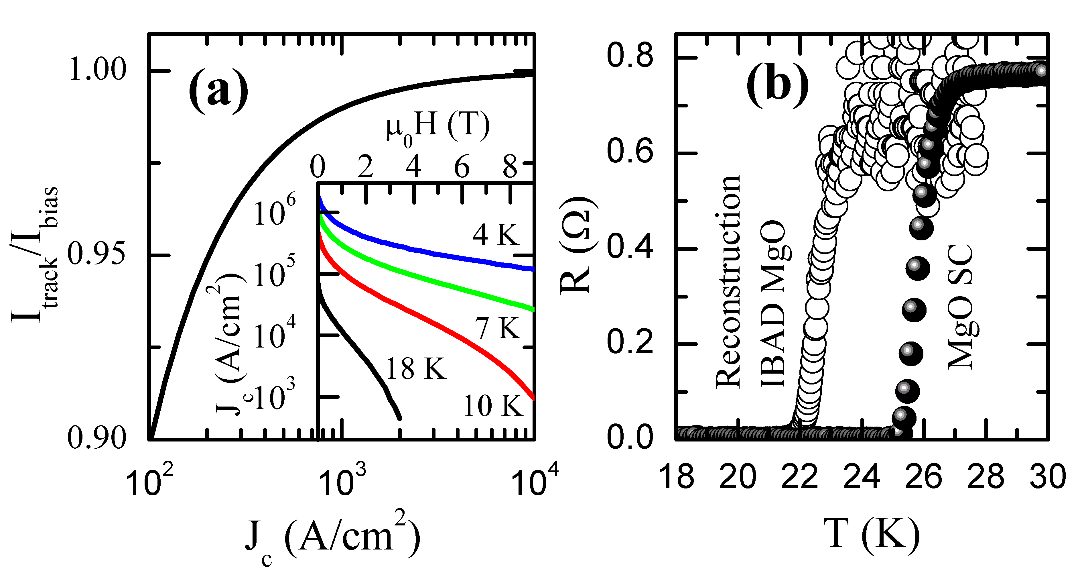
Since the combined resistive transition has to be continuous, and have to be equal at their extremum which gives 7.8 . The reconstructed superconducting transition using these values is displayed in fig.4(b) and compared to a Ba-122/Fe bilayer on MgO-SC prepared under comparable conditions. The , defined as 50% of the normal resistivity at 30 K, was evaluated to 23 K which is slightly lower compared to films prepared on MgO-SC with K. The origin of this deviation is not uniquely assignable. Both, a reduced preparation temperature while using metal substrates and additional doping of Ba-122 by transition metal ions will affect . The simulation of is in very good agreement with the observed transition of tape (B) using eq.(2) with a Ba-122/Fe normal state resistance of 0.7 and the determined values for and as displayed in fig.1(b).
Finally, we etched a 1 mm wide and 1 mm long track in section B (fig.3(a)) for the determination of . We made the following assumption in order to estimate the influence of this geometry on the fraction of current flowing through the tape at the determined of the track: Currents for which the track enters the flux flow state are still loss free in the remaining part of the Ba-122 section A and C due their larger width. Therefore one can reduce the resistor network to a simple parallel circuit, where the current through the track () is defined as and the fraction shunted by the tape is ). The field criterion with the length of the track mm was set to 10-6 V/cm for the determination of . The resulting ratio of is given in fig.4(a), where for higher than 1 kA/cm2 99% of the current passes the superconducting track. For the self field of the film, which is higher than 70 kA/cm up to K (fig.4(a), inset), this correction is negligible.
In summary we have demonstrated that a peak in the resistive transition appears when the electrical barrier resistance between tape and Ba-122/Fe bilayer is reduced. A simple resistor network array describes all main features of the measured behavior. The error in the determination of the self field is negligible for values higher than 1 kA/cm2. The results indicate that a reduced buffer layer thickness has no detrimental effect on the superconducting properties of Ba-122. A thin electrical conducting barrier layer may even be beneficial as it provides an effective protection of the superconducting film in case is exceeded, as the majority of the current will be shunted by the tape.
This work was partially supported by the Deutsche Forschungsgesellschaft and SuperIron, founded by the European Commission.
References
- (1) A. Goyal, M. Parans Paranthaman and U. Schoop, MRS Bull. 29 (2004), 552-561.
- (2) Y. Iijima, K. Kakimoto, Y. Yamada, T. Izumi, T. Saitoh and Y. Shiohara, MRS Bull. 29 (2004), 564-571.
- (3) K. Iida, J. Hänisch, S. Trommler, V. Matias, S. Haindl, F. Kurth, I. L. del Pozo, R. Hühne, M. Kidszun, J. Engelmann, L. Schultz, and B. Holzapfel, Applied Physics Express 4 (2011), 013103.
- (4) T. Katase, H. Hiramatsu, V. Matias, C. Sheehan, Y. Ishimaru, T. Kamiya, K. Tanabe and H. Hosono, App. Phys. Lett. 98, (2011), 242510.
- (5) Q. Li, W. Si and I. K. Dimitrov, Rep. Prog. Phys. 74 (2011), 124510.
- (6) C. Sheehan, Y. Jung, T. Holesinger, D. M. Feldmann, C. Edney, J. F. Ihlefeld, P. G. Clem, and V. Matias, App. Phys. Lett. 98 (2011), 071907.
- (7) V. Matias, J. Hänisch, E. J. Rowley, and K. Güth, J. Mater. Res. 24 (2009), 125.
- (8) V. Matias, E. J. Rowley, Y. Coulter, B. Maiorov,T. Holesinger, C. Yung, V. Glyantsev, B. Moeckly, SUST 23 (2010), 014018 (5pp).
- (9) T. Thersleff, K. Iida, S. Haindl, M. Kidszun, D. Pohl, A. Hartmann, F. Kurth, J. Hänisch, R. Hühne, B. Rellinghaus, L. Schultz, and B. Holzapfel, App. Phys. Lett. 97 (2010), 022506.
- (10) K. Iida, S. Haindl, T. Thersleff, J. Hänisch, F. Kurth, M. Kidszun, R. Hühne, I. Mönch, L. Schultz, B. Holzapfel, and R. Heller, Appl. Phys. Lett. 97, (2010), 172507.
- (11) N. Ni, M. E. Tillman, J.-Q. Yan, A. Kracher, S. T. Hannahs, S. L. Bud’ko, and P. C. Canfield, Phys. Rev. B 78 (2008), 214515.
- (12) J. Bass, K.-H. Hellwege (ed.), J. L. Olsen (ed.)., Landolt-Börnstein - Group III Condensed Matter, Springer Materials, p. 109 & p. 279, Fig. 163-170, DOI: 10.1007/b29240.
- (13) J. Lu, E. S. Choi, and H. D. Zhou, J. App. Phys. 103, (2008), 064908
- (14) K. Iida, J. Hänisch, R. Hühne, F. Kurth, M. Kidszun, S. Haindl, J. Werner, L. Schultz, and B. Holzapfel, App. Phys. Lett. 95, (2009), 192501.