Deformation and scattering in graphene over substrate steps
Abstract
The electrical properties of graphene depend sensitively
on the substrate. For example, recent measurements of
epitaxial graphene on SiC show resistance arising from
steps on the substrate.
Here we calculate the deformation of graphene at substrate steps,
and the resulting electrical resistance, over a wide range of step heights.
The elastic deformations contribute only a very small resistance at the step.
However, for graphene on SiC(0001) there is strong substrate-induced doping,
and this is substantially reduced on the lower side of the step
where graphene pulls away from the substrate.
The resulting resistance explains the experimental measurements.
The advance of very high speed graphene electronicsAvouris (2010); Lin et al. (2011a) depends on understanding and controlling the interaction of graphene with the supporting substrate. Electron mobility can vary over many orders of magnitude depending on the substrate Neto et al. (2009); Dean et al. (2010); Berger et al. (2006). Among other factors, morphological deformations of the graphene may limit mobility Dimitrakopoulos et al. (2011); Lin et al. (2011b); Bryan et al. (2011); Ji et al. (2011); Kim et al. (2011). It is therefore important to determine how the substrate morphology affects transport in supported graphene.
Epitaxial graphene on SiC provides an ideal system in which to study the role of substrate morphology. SiC is a promising substrate because, in contrast to other approaches, it allows growth of epitaxial graphene directly on an insulating substrate Emtsev et al. (2009). However, epitaxial graphene on SiC substrates generally exhibits smaller carrier mobilities than exfoliated graphene on SiO2 substrates Berger et al. (2006); Emtsev et al. (2009); Tedesco et al. (2009); Robinson et al. (2009a). The reason for this difference is not fully understood, but SiC substrates exhibit a high density of multilayer steps, which are implicated in the lower mobility. Several experiments show that resistance increases with step densityDimitrakopoulos et al. (2011), step heightsJi et al. (2011) and step bunchingLin et al. (2011b); Bryan et al. (2011); and the local electrical resistance associated with individual substrate steps has recently been measured Ji et al. (2011), by scanning potentiometry in a scanning tunneling microscope.
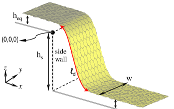
Here we study graphene over an abrupt substrate step, as illustrated in Fig. 1, calculating both the structural deformation and the resulting electrical resistance. The results are directly applicable to epitaxial graphene on SiC, and also show more generally how the morphology affects electrical transport. We find that very little resistance arises directly from the structural deformations, despite the strong curvature of graphene as it passes over a step. For SiC, we nevertheless find a substantial resistance associated with the step, in good agreement with experimentJi et al. (2011). This resistance arises almost entirely from the electrical coupling between the graphene and substrate, which varies sharply in the vicinity of the step. Thus morphology plays a qualitatively different and far more important role in substrates such as SiC that dope the substrate or otherwise couple strongly, than it does for substrates such as SiO2 that are electrically passive.

We begin by determining the graphene geometry as it passes over a substrate step. The graphene deformation is determined by a balance between the van der Waals interaction, which favors conforming to the substrate, and elasticity, which favors keeping the graphene flat and smooth. Since the displacement field can vary on the atomic scale, we use an atomistic valence force model (VFM) to describe the elastic deformations Perebeinos and Tersoff (2009). The van der Waals interaction between graphene and substrate is modeled with the Lennard-Jones (LJ) 6-12 potential Girifalco and Lad (1956). The parameters for our LJ model are determined by setting the equilibrium distance between graphene and substrate to ÅMattausch and Pankratov (2007), and the binding energy to meV per atom Girifalco and Lad (1956); Zacharia et al. (2004). The total energy is then simply the sum of these two contributions, .
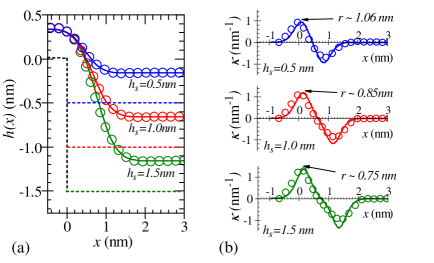
We calculate the minimum-energy geometry for graphene over a wide range of step height , allowing the graphene to slide to relax any in-plane strain. The relaxed geometries for three step heights typical of SiC are plotted in Fig. 2a. The presence of the atomic step increases the graphene area compared to when the substrate is flat. The extra length increases with and was found to be , , and nm respectively. The nonlinear dependence reflects the increasing distortion (steeper slope) with increasing step height. The maximum slope is of order 1, confirming the need for a fully numerical treatment.
We find that the calculated geometries can be well approximated by a simple error function,
| (1) |
As shown in Fig. 2b, even the variation in curvature across the step is well described by this simple functional form. The only noticeable discrepancy is that the error function is symmetric, while in the full calculation there is a slight asymmetry, with the maximum curvature induced at the upper edge of the step. For step height nm, we find a maximum curvature equivalent to that of a carbon nanotube of diameter nm.
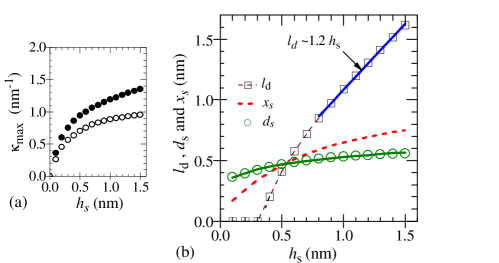
The maximum curvature as a function of step height is plotted in Fig. 3a, for both the lower and upper edge of the step. It is proportional to in the small limit. For the lower edge, the limit of large corresponds to the well-known problem of peeling Landau and Lifshitz (1986). In this limit, approaches nm-1, where is area per carbon atom and eV Perebeinos and Tersoff (2009) is the bending rigidity.
Figure 3b summarizes the dependence of the graphene deformation on step height , in terms of the parameters of Eq. 1. For a given step height, the characteristic step width determines the maximum radius of curvature . Another relevant lengthscale is the length over which the graphene is detached from the substrate. For concreteness we define to be the length of graphene separated by or more from the substrate surface. Fig. 3b shows that remains zero at small but begins to increase rapidly for . At larger step height we find that , which proves important in later discussions.


Geometry-induced scattering: Curvature results in bandstructure changes that can scatter electrons near the step. To examine this effect, after performing the geometry relaxation, we construct the Hamiltonian within a nearest-neighbor Slater-Koster parameterized tight-binding model Tomanek and Louie (1988). We then calculate the transmission and the electrical resistance using the non-equilibrium Green’s function formalismDatta (1997); Di Ventra (2008) in the limit of small voltage across the step and no inelastic scattering at the step. We use the known Fermi levelBostwick et al. (2007); Mattausch and Pankratov (2007) of eV for graphene on SiC (0001).
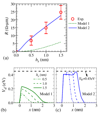
Since the maximum curvature increases with step height , the resistance also increases. For a step height of nm, we obtain a resistance -m. Figure 4a includes results of a recent experimentJi et al. (2011), which employed scanning potentiometry in a scanning tunneling microscope to resolve the resistance in graphene due to individual substrate steps. The measured resistance has roughly linear dependence with step height , -m for each nanometer step height. Evidently, the resistance due to curvature alone cannot account for this large . While - hybridization can result in new scattering states in the vicinity of Dirac point Blase et al. (1994), this effect is significant only when ÅBlase et al. (1994). Even for a very high step of nm, we find that the minimum radius of curvature only shrinks to Å if we assume a much stronger van der Waals attraction, with a binding energy meV, which seems unphysical.
In our calculations thus far, we have ignored possible in-plane strain inhomogeneities, which is known to result in electron scattering Fogler et al. (2008); Pereira and Neto (2009). Due to the different thermal expansion coefficient between graphene and SiC, graphene can acquires a residual biaxial strain upon cooling if sliding is suppressed. Then due to the nonplanar geometry, graphene at the step could experience a uniaxial stress relative to the rest of the sheet. Graphene on SiC substrates is reported to have strains from as measured by Raman spectroscopy Robinson et al. (2009b). To estimate a very conservative upper bound for due to strain inhomogeneity, we consider a local tensile strain of along the detached region, with the step along the zigzag direction where the scattering effect is largest Fogler et al. (2008). The result is -m. Thus some source of scattering much stronger than the geometrical deformations must be present to account for the measured resistance.

Electrostatic doping effects: It is well known that when contacting graphene with metals, a difference in workfunction results in electrostatic doping Huard et al. (2008); Khomyakov et al. (2009); Giovannetti et al. (2008). In the case of SiC(0001), a similar doping occurs from the carbon buffer layer, which has a high density of weakly dispersive interface states Varchon et al. (2007); Mattausch and Pankratov (2007). This can be described by a capacitor model including quantum capacitance Kopylov et al. (2010),
| (2) |
where is the electron density in graphene, is the workfunction difference between the carbon buffer layer and graphene, is the distance between them, and is the buffer-layer density of states. We denote this as “Model 1”. In view of the flat bands Varchon et al. (2007); Mattausch and Pankratov (2007), we take the limit of large and we adjust to reproduced the known doping at , corresponding to heavy n-doping Bostwick et al. (2007); Mattausch and Pankratov (2007), with a Fermi level eV. The vertical displacement changes the capacitive coupling, leading to doping variations. Substituting the relaxed geometry into Eq. 2, we calculate these variations. The associated potential shifts are shown in Fig. 4b for different step heights. Increasing step height leads to larger detachment and doping variations. This translates to an increased as shown in Fig. 4a, still somewhat smaller than reported experimentally, but far larger than the scattering mechanisms previously discussed.
In studies of metal induced doping of graphene, Khomyakov and co-workers Khomyakov et al. (2009); Giovannetti et al. (2008) reported that Eq. 2 could not properly describe the ab initio calculations of graphene on metals, presumably due to quantum mechanical effects such as wavefunction overlap and correlations They suggested that the accuracy of Eq. 2 can be improved by the modification Khomyakov et al. (2009); Giovannetti et al. (2008)
| (3) |
with and approximated as independent of the metal species. Since the corresponding values for SiC are not known, and the buffer layer has a large density of states the Fermi level, we simply use the values reported for metals in Refs. Khomyakov et al. (2009); Giovannetti et al. (2008).
This “Model 2” gives a stronger doping variation than the classical electrostatic model, as show in Fig. 4c. The corresponding resistance is also increased for Model 2, as shown in Fig. 4a, giving excellent agreement with experiment. Indeed, we consider the degree of quantitative agreement between “Model 2” and the experimental data to be somewhat fortuitous. Nevertheless, it is striking that, using the best approximations available, the modulation of local doping by the step can account for the observed resistance, while other mechanisms are all far too small.
In principle there could be additional electronic states associated with the step that would change the resistance; but it is not necessary to assume such states in order to explain the resistance. Here we assumed the vertical surface of the atomic step to be electrically inert. This is reasonable since the SiC(000) surface is electrically inert, and the extra states are associated with the buffer layer. In addition, our results are relatively robust against the uncertainties in the bending stiffness and the van der Waals binding energy. For example, if we assume an unreasonably large meV instead of meV, the detachment length for the largest step height decreases from nm to nm, suggesting a decrease in resistance of only . A factor of 2 change in the assumed bending stiffness would have a similar effect.
As seen in Fig. 4b, the graphene is almost fully depleted of carriers in the detached region. This suggests a simple model where the graphene is completely undoped over the detachment length . Our situation then resembles the problem of minimum conductivity, often discussed in the literatureTworzydlo et al. (2006). Transport in this regime is mediated by evanescent modes, but instead of an exponential decay the graphene bandstructure leads to a unique linear (“pseudo-diffusive”) behavior Tworzydlo et al. (2006), where . This represents the upper bound for resistance due to doping variations, where the doping goes to zero in the detached region, and overestimates the calculations of “Model 2” by about . Combining this with our previous result that explains the linear scaling of resistance with step height (i.e. ) observed in experiment.
Conclusions: We examined the structural deformation of graphene crossing over a substrate step, and the various intrinsic mechanisms that may cause electron scattering at the step. We found that deformation gives only a small electron scattering. For graphene on SiC, where the substrate induces considerable doping, the dominant mechanism is rather the abrupt variation in potential and doping due to detachment of the graphene from the substrate as it passes over a step. Our result reconcile with the various experimental observations, i.e. that increases with step densityDimitrakopoulos et al. (2011), step heightsJi et al. (2011), step bunchingLin et al. (2011b); Bryan et al. (2011), all of them are manifestations of increasing .
Acknowledgements We thank the authors of Ref. Ji et al. (2011) for providing experimental data prior to publication. TL acknowledges use of a computing cluster provided by Network for Computational Nanotechnology, and partial funding from INDEX-NRI.
References
- Avouris (2010) P. Avouris, Nano Lett. 10, 4285 (2010).
- Lin et al. (2011a) Y. M. Lin, A. V. Garcia, S. J. Han, D. B. Farmer, I. Meric, Y. Sun, Y. Wu, C. Dimitrakopoulos, A. Grill, P. Avouris, et al., Science 332, 1294 (2011a).
- Neto et al. (2009) A. H. C. Neto, F. Guinea, N. M. Peres, K. S. Novoselov, and A. K. Geim, Rev. Mod. Phys. 81, 109 (2009).
- Dean et al. (2010) C. R. Dean, A. F. Young, I. Meric, C. Lee, L. Wang, S. Sorgenfrei, K. Watanabe, T. Taniguchi, P. Kim, K. L. Shepard, et al., Nature Nano. 5, 722 (2010).
- Berger et al. (2006) C. Berger, Z. Song, X. Li, X. Wu, N. Brown, C. Naud, D. Mayou, T. Li, J. Hass, A. Marchenkov, et al., Science 312, 1191 (2006).
- Dimitrakopoulos et al. (2011) C. Dimitrakopoulos, A. Grill, T. McArdle, Z. Liu, R. Wisnieff, and D. A. Antoniadis, Appl. Phys. Lett. 98, 222105 (2011).
- Lin et al. (2011b) Y. M. Lin, D. B. Farmer, K. A. Jenkins, Y. Wu, J. L. Tedesco, R. L. Myers-Ward, C. R. Eddy, D. K. Gaskill, C. Dimitrakopoulos, and P. Avouris, To appear in IEEE Elec. Dev. Lett. (2011b).
- Bryan et al. (2011) S. E. Bryan, Y. Yang, and R. Murali, J. Phys. Chem. C 115, 10230 (2011).
- Ji et al. (2011) S. Ji, J. B. Hannon, R. M. Tromp, V. Perebeinos, J. Tersoff, and F. M. Ross, Nature Materials (online) (2011).
- Kim et al. (2011) K. Kim, Z. Lee, B. D. Malone, K. T. Chan, B. Aleman, W. Regan, W. Gannett, M. F. Crommie, M. L. Cohen, and A. Zettl, Phys. Rev. B 83, 245433 (2011).
- Emtsev et al. (2009) K. V. Emtsev, A. Bostwick, K. Horn, J. Jobst, G. L. Kellogg, L. Ley, J. L. McChesney, T. Ohta, S. A. Reshanov, J. Rohrl, et al., Nature Mat. 8, 203 (2009).
- Tedesco et al. (2009) J. L. Tedesco, B. L. VanMil, R. L. Myers-Ward, J. M. McCrate, S. A. Kitt, P. M. Campbell, G. G. Jernigan, J. C. Culbertson, C. R. Eddy, and D. K. Gaskill, J. Phys. Chem. C 95, 122102 (2009).
- Robinson et al. (2009a) J. A. Robinson, M. Wetherington, J. L. Tedesco, P. M. Campbell, X. Weng, J. Stitt, M. A. Fanton, E. Frantz, D. Snyder, B. L. VanMill, et al., Nano Lett. 9, 2873 (2009a).
- Perebeinos and Tersoff (2009) V. Perebeinos and J. Tersoff, Phys. Rev. B 79, 241409(R) (2009).
- Girifalco and Lad (1956) L. A. Girifalco and R. A. Lad, J. Chem. Phys. 25, 693 (1956).
- Mattausch and Pankratov (2007) A. Mattausch and O. Pankratov, Phys. Rev. Lett. 99, 076802 (2007).
- Zacharia et al. (2004) R. Zacharia, H. Ulbricht, and T. Hertel, Phys. Rev. B 69, 155406 (2004).
- Landau and Lifshitz (1986) L. D. Landau and E. M. Lifshitz, Butterworth-Heinemann, Course of Theoretical Phys. 7, 45 (1986).
- Tomanek and Louie (1988) D. Tomanek and S. G. Louie, Phys. Rev. B 37, 8327 (1988).
- Datta (1997) S. Datta, Cambridge University Press (1997).
- Di Ventra (2008) M. Di Ventra, Cambridge University Press (2008).
- Bostwick et al. (2007) A. Bostwick, T. Ohta, T. Seyller, K. Horn, and E. Rotenberg, Nat. Phys. 3, 36 (2007).
- Blase et al. (1994) X. Blase, L. X. Benedict, E. L. Shirley, and S. G. Louie, Phys. Rev. Lett. 72, 1878 (1994).
- Fogler et al. (2008) M. M. Fogler, F. Guinea, and M. I. Katsnelson, Phys. Rev. Lett. 101, 226804 (2008).
- Pereira and Neto (2009) V. M. Pereira and A. H. C. Neto, Phys. Rev. Lett. 103, 046801 (2009).
- Robinson et al. (2009b) J. A. Robinson, C. P. Puls, N. E. Staley, J. P. Stitt, M. A. Fanton, K. V. Emtsev, T. Seyller, and Y. Liu, Nano Lett. 9, 964 (2009b).
- Huard et al. (2008) B. Huard, N. Stander, J. A. Sulpizio, and D. Goldhaber-Gordon, Phys. Rev. B 78, 121402(R) (2008).
- Khomyakov et al. (2009) P. A. Khomyakov, G. Giovannetti, P. C. Rusu, G. Brooks, J. van den Brink, and P. J. Kelly, Phys. Rev. B 79, 195425 (2009).
- Giovannetti et al. (2008) G. Giovannetti, P. A. Khomyakov, G. Brooks, V. M. Karpan, J. van den Brink, and P. J. Kelly, Phys. Rev. Lett. 101, 026803 (2008).
- Varchon et al. (2007) F. Varchon, R. Feng, J. Hass, X. Li, N. Nguyen, C. Naud, P. Mallet, J. Y. Veuillen, C. Berger, E. H. Conrad, et al., Phys. Rev. Lett. 99, 126805 (2007).
- Kopylov et al. (2010) S. Kopylov, A. Tzalenchuk, S. Kubatkin, and V. Fal’ko, Appl. Phys. Lett. 97, 112109 (2010).
- Tworzydlo et al. (2006) J. Tworzydlo, B. Trauzettel, M. Titov, A. Rycerz, and C. W. J. Beenakker, Phys. Rev. Lett. 96, 246802 (2006).