School of Physics, University of New South Wales, Sydney NSW 2052, Australia
Realizing lateral wrap-gated nanowire FETs: Controlling gate length with chemistry rather than lithography
Abstract
An important consideration in miniaturizing transistors is maximizing the coupling between the gate and the semiconductor channel. A nanowire with a coaxial metal gate provides optimal gate-channel coupling, but has only been realized for vertically oriented nanowire transistors. We report a method for producing laterally oriented wrap-gated nanowire field-effect transistors that provides exquisite control over the gate length via a single wet etch step, eliminating the need for additional lithography beyond that required to define the source/drain contacts and gate lead. It allows the contacts and nanowire segments extending beyond the wrap-gate to be controlled independently by biasing the doped substrate, significantly improving the sub-threshold electrical characteristics. Our devices provide stronger, more symmetric gating of the nanowire, operate at temperatures between 300 to 4 Kelvin, and offer new opportunities in applications ranging from studies of one-dimensional quantum transport through to chemical and biological sensing.
Keywords: Nanowire, field-effect transistor, wrap-gate, lateral.
Self-assembled semiconductor nanowires offer great promise as one-dimensional elements for a range of future electronic device applications, from next-generation computer technologies 2, 3 to energy generation and biological/chemical sensing. 4, 5 Vertically oriented nanowire field-effect transistors have received considerable attention due to the possibility of producing high density arrays, 2, 6, 7, 8, 9 but the fabrication is challenging, involving many process steps to define the contacts and gates. 10 Fundamental studies of transport in nanowire-based quantum devices have instead focused on nanowires oriented laterally on the substrate, mostly due to the relative ease of fabrication. However, the common routes to gating laterally oriented nanowires – namely using the substrate, 11, 12 insulated metal gates deposited directly underneath the nanowire, 13 or gates deposited over an oxide-coated nanowire (omega gates) 14, 15 – make calculation of the gate-channel capacitance difficult and lead to substantial charge inhomogeneity within the nanowire. 16 Since the ideal gate configuration for a nanowire field-effect transistor (NW-FET) is a coaxial ‘wrap-gate’, the development of lateral wrap-gate NW-FETs is highly desirable. It is a challenging goal, because depositing gate metal underneath a nanowire already sitting laterally on a substrate is a formidable undertaking, and using a nanowire where the wrap-gate exists prior to deposition onto a substrate entails the difficulty of exposing the ends of the nanowire to make contacts that are not electrically shorted to the wrap-gate.
We have developed a surprisingly simple route to producing lateral wrap-gated NW-FETs that builds upon existing methods for fabricating vertical wrap-gate NW-FETs 2 and exploits the fortuitous tendency for etchants to undercut a resist, gaining access to the wrap-gate via the openings made for the source and drain contacts using electron-beam lithography. A major advantage is that we can precisely control the gate length over a wide range via a single wet-etch step. Our method requires no additional lithography compared to the current state-of-the-art for gating lateral NW-FETs, 14, 15 and results in NW-FETs with improved sub-threshold characteristics.
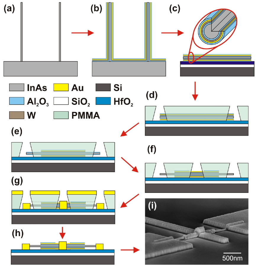
The process used is presented in Fig. 1. InAs nanowires nm in diameter and m long were grown by chemical beam epitaxy (Fig. 1(a)). 17 The nanowires contain a nm long InAs0.95P0.05 segment, added for a separate experiment, between two m long InAs segments. The as-grown nanowires were coated with nm of \ceAl2O3 by atomic layer deposition (ALD), a metal wrap-gate consisting of nm of tungsten and nm of gold by DC sputtering, and a further nm of \ceAl2O3 as an outer insulator layer (Fig. 1(b)). This outer oxide is superfluous electrically, but essential to the fabrication – we transfer the nanowires to a heavily doped Si substrate (Fig. 1(c)) using the tip of a small piece of lab-wipe, and the coated nanowires will not adhere to the paper fibres without this outer oxide. The device substrate features a nm thermally-grown \ceSiO2 layer covered with nm of \ceHfO2 by ALD, and is pre-patterned with large-scale leads and alignment markers for electron-beam lithography (EBL) prior to deposition of the nanowires. The nm \ceHfO2 layer is also essential to the fabrication – \ceHfO2 etches much more slowly than \ceAl2O3 and \ceSiO2 in buffered hydrofluoric acid (BHF), and thus the \ceHfO2 layer protects the \ceSiO2 substrate insulation during two BHF etches used to remove sections of the \ceAl2O3 layers coating the nanowire/wrap-gate. After nanowire deposition, the device is coated with nm of polymethylmethacrylate (PMMA) resist, and the source and drain leads to a selected nanowire are defined by EBL (Fig. 1(d)).
The W/Au wrap-gate and \ceAl2O3 layers initially extend the full length of the nanowire, jutting out into the EBL-defined source and drain contact regions (Fig. 1(d)). Three subsequent wet etches are administered at this stage (Fig. 1(e)), and it is the second, an iodine-based gold etch, 18 that ultimately sets the wrap-gate length. The first is a s etch in BHF at room temperature to strip back the outer \ceAl2O3 layer, exposing the wrap-gate. This is followed by the Au etch, which we describe in more detail below. The third etch in \ceH2O2 at C for s removes any exposed tungsten in the wrap-gate. The various Au etch solutions are made from a stock solution containing g \ceKI and g \ceI2 dissolved in mL of deionized \ceH2O (Millipore M.cm). This stock solution has an extremely high etch rate m/min, 19 and we use further dilutions ranging from to in deionized \ceH2O to ensure that the etch can be applied with accurate control within a reasonable etch time ( s).
The lead connecting the wrap-gate is defined in a second stage of EBL on the same resist (Fig. 1(f)), but is omitted for the devices made to study the dependence of gate length on the etch parameters (i.e., Figs. 2/3). A final BHF etch ( s at room temperature) is then performed to simultaneously remove the exposed inner \ceAl2O3 layer at the source and drain contacts and the exposed outer \ceAl2O3 layer where the gate lead intersects the wrap-gate (Fig. 1(f)). Electrodes consisting of nm Ni and nm Au were deposited by thermal evaporation in vacuum (Fig. 1(g)), immediately following a contact passivation step involving a s immersion in an aqueous \ce(NH4)2S solution at C. 20 Finally, lift-off of the excess metal and PMMA is performed to obtain the completed device structure shown schematically in Fig. 1(h). A scanning electron microscope (SEM) image of a completed device made using the Au etch for s is shown in Fig. 1(i). A corresponding top-view of a similar device appears in the supplementary information (Fig. S1), and careful inspection of contrast changes along the wrap-gate reveals where the outer oxide has been stripped to expose the wrap-gate for contacting. The ability to define all three leads to the nanowire, and set the gate length, using a single resist layer and one metal evaporation makes this a very time efficient fabrication process.
Two parameters govern the Au etch – concentration and time – and in Figs. 2 and 3 we demonstrate that both provide excellent fine control of the gate length. As the measurable parameter for gate length we use the separation between the gate edge and the nearest contact in the completed device, obtained from scanning electron microscopy studies. The gate-contact separation is independent of the nanowire length, as well as of the EBL-defined source-drain contact separation providing that the Au etch undercut is not more than half the source-drain contact separation. For each data point in Fig. 2(a) and 3(a) we made a ‘chip’ containing lateral wrap-gate NW-FETs, each with two gate-contact separations at the source and drain. We obtained an average yield of , such that each point in Fig. 2(a) and Fig. 3(a) is the average of individual measurements for a given Au etch concentration/time, with the other three wet etches held constant at the specifications given earlier.
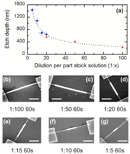
Figure 2(a) shows the resulting etch depth versus Au etch concentration, with SEM images of representative devices for each concentration presented in Figs. 2(b-g). In each case the Au etch time is s. At the lowest concentration of stock solution to \ceH2O, the wrap-gate almost spans the entire distance between source and drain contacts (see Fig. 2(b)). A fortuitous aspect of our method is that the undercutting action of the etch always prevents shorting of the gate to the contacts, in contrast to other self-aligned methods for creating quantum wires where gate-contact shorting is a significant problem. 21, 22 Higher Au etchant concentration causes increased under-etching at the contact openings, resulting in a wrap-gate that is much shorter than the lithographically-defined contact separation. At sufficiently high concentration the wrap-gate becomes extremely short (see Fig. 2(g)), and can be eliminated entirely (not shown), leading to a malfunctioning device if a gate lead is deposited. The data in Fig. 2(a) roughly follows a power law dependence, indicating an effective route to wide-ranging control over the gate length. Varying the etch time provides an alternative control, as demonstrated in Fig. 3(a) for the dilution etch, with corresponding typical devices shown in Figs. 3(b)-(e). Although changing the dilution and time have a similar outcome, in a practical device fabrication setting, changes in concentration would be more suitable for enacting coarse control over wrap-gate length, with the etch time providing a route to finer control that enables devices with precise gate lengths to be produced.
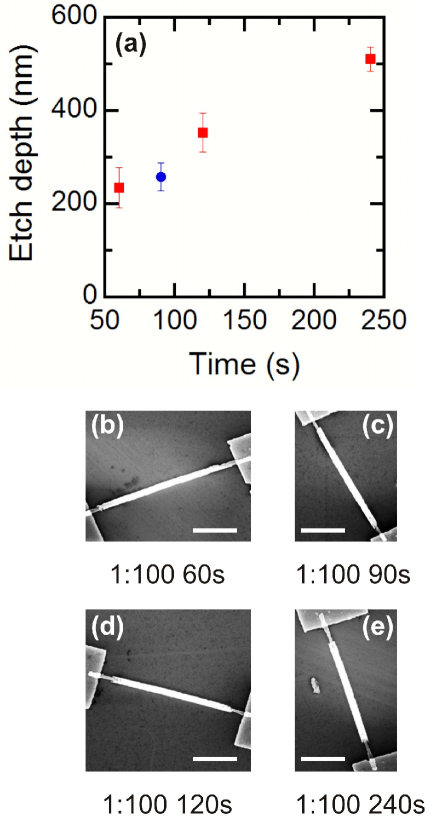
The influence that the other three wet etch processes have on the gate length is an important additional question in light of our findings about the Au etch. To confirm that the Au etch is indeed the sole determinant of gate length, we made three additional chips, each with a Au etch applied for s, but with one of the three other wet-etches in the process applied for twice the time specified earlier (i.e., BHF etches of inner/outer gate insulator for s or \ceH2O2 etch for W wrap-gate metal for s). Doubling the time for any of these etches has a negligible effect on the gate-contact separation for resulting NW-FETs (see Supplementary Fig. S2 for data). In contrast, doubling the time for the Au etch increases the gate-contact separation by based on the data in Fig. 3. This does not mean that the specifics of these three wet etches can be neglected, if these etches are insufficient or overly extended then working devices are not obtained, but the process is robust to small fluctuations in these three etches compared to the Au etch.
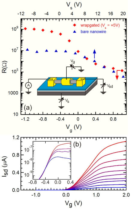
To demonstrate the electrical properties of our wrap-gate NW-FETs, two chips A and B were prepared in separate processing runs with the dilution Au etchant applied for and s, respectively. A third chip C containing conventional substrate-gated NW-FETs (i.e., no wrap-gate) using nanowires from the same growth was also prepared. We used the measurement circuit shown inset to Fig. 4(a) with the source-drain current measured at the drain contact as a function of biases , and applied to the source, wrap-gate and substrate, respectively. In Fig. 4(a) we plot the measured two-terminal resistance versus (blue triangles – top axis) for a substrate-gated NW-FET. The resistance increases from k at V, saturating at M for negative . The measured resistance for the wrap-gate NW-FET versus (red diamonds – bottom axis) with held at V is also shown. At V, k, which compares favorably with M obtained for the substrate-gated NW-FET under corresponding conditions (i.e., V). The wrap-gate NW-FET reaches an off-state resistance G, two orders of magnitude higher than the substrate-gated NW-FET, with a smaller gate-range, demonstrating that the wrap-gate allows much stronger gating while freeing the substrate to be used for maintaining the quality of the contacts.
A common quality metric for NW-FETs is the field-effect mobility , where is the transconductance and is the gate capacitance. 23 Before comparing the mobility for our devices, we note that fundamental differences in device geometry combined with difficulties in accurately estimating the capacitance due to the dual-layer \ceSiO2/\ceHfO2 substrate insulation, substrate gating of regions outside the wrap-gate, and the overestimation 16 of the capacitance by the standard expression for a cylindrical conductor on a planar substrate 24, 25 mean that the values obtained are semi-quantitative estimates at best. For the substrate-gated NW-FET we obtain cm2/Vs for a contact separation of m and gate capacitance of aF obtained using the standard cylinder-on-plane model. 24, 25 This mobility is low compared to that typically found for substrate-gated InAs NW-FETs ( cm2/Vs). We initially attributed this to the InAs0.95P0.05 segment, however, Lind et al. reported cm2/Vs for substrate-gated InAs NW-FETs containing a nm InAs0.7P0.3 segment, 26 which presents a much higher transport barrier. Hence we instead suspect that the reduced mobility is due to surface effects, since our substrates have a \ceHfO2 surface layer unlike the devices studied by Lind et al. 26 For the wrap-gate NW-FET we obtain cm2/Vs for a m channel length and fF gate capacitance calculated using a coaxial capacitor model, ignoring end-effects or capacitance contributions from the nanowire regions extending outside the wrap-gate. The mobility is lower than that for the substrate-gated NW-FET, and we attribute this to surface states at the nanowire/inner oxide interface. We note that values of similar magnitude were reported for vertical wrap-gated InAs NW-FETs and likewise attributed to interface effects. 9 Interface problems in wrap-gate NW-FETs are a well-known issue, and their passivation is a goal for future development of these devices. 2, 23
Our wrap-gate NW-FETs make up for their unexceptional mobility with excellent sub-threshold characteristics, which are of interest for sensing applications. 5 Figure 4(b) shows transfer characteristics for two wrap-gate NW-FETs with very similar characteristics aside from a difference in threshold voltage. The main panel of Fig. 4(b) shows plots of versus obtained for between and mV, demonstrating the high quality characteristics afforded by using the biased substrate to maintain stable, low resistance contacts while depleting the nanowire using the wrap-gate. The threshold voltage for this device is mV but we typically find values ranging from to V, and a survey of the working devices on Chip A gave an average V. This spread in may be due to diameter variation in the nanowires used, 27 but may be related to charge trapping at the InAs/\ceAl2O3 interface, and we observe occasional discrete shifts in consistent with this, particularly at low temperature.
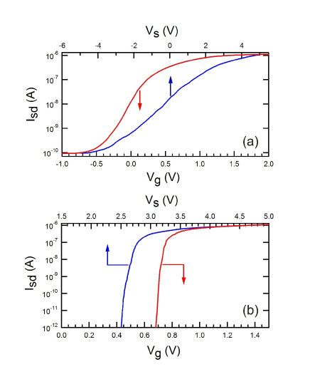
We demonstrate that the wrap-gate operates independently of the substrate in Fig. 4(b) inset by plotting versus for differing . When the wrap-gated region is in the on-state (upper right), is the dominant influence over and small changes in have little impact. For V, the wrap-gate dominates, with traces for each overlapping. To directly compare the relative effect of the wrap-gate and substrate, in Fig. 5(a) we show the transfer characteristics for both the wrap-gate (red trace – bottom axis) and the substrate (blue trace – top axis), starting from a common configuration with V and V. In both cases, falls with decreasing gate bias, saturating at an off-state value of pA, corresponding to an on-off ratio . The substrate data is slightly noisier than the wrap-gate data for low , as expected since substrate biasing also has a detrimental effect on the contacts. The wrap-gate inverse sub-threshold slope is mV/decade, nearly an order of magnitude better than the mV/decade obtained using the substrate. It is interesting to compare this with results by Lind et al. 26 Their substrate inverse sub-threshold slope decreased from V/decade to mV/decade on adding the InAsP segment, and they predicted further substantial improvement if the InAsP segment is enclosed within a wrap-gate. 26 Our data supports this prediction, and is consistent with recent data from a vertical wrap-gate NW-FET with a nm InAs0.8P0.2 segment that gave inverse sub-threshold slopes as low as mV/decade. 28 On a device-to-device basis the wrap-gate inverse sub-threshold slope is more consistent than with an average slope of mV/decade across the devices on Chip A. Although the current record for vertical wrap-gate NW-FETs is mV/decade, 10 values from to mV/decade are typical, 9, 26, 27, 29, 30 and heavily dependent on careful optimization of the nanowire/insulator interface. 9, 10, 28, 30
The ability to achieve strong, symmetric gating of a section of nanowire whilst using the substrate to ensure a low contact resistance makes lateral wrap-gate NW-FETs very interesting for studying one-dimensional quantum transport phenomena at low temperature. To demonstrate that our devices work well at low temperatures, in Fig. 5(b) we present transfer characteristics for the wrap-gate with V (red trace – bottom axis) and the substrate gate with V (blue trace – top axis) obtained from Chip B at Kelvin. In both cases the inverse sub-threshold slope has improved markedly, to mV/decade for the wrap-gate, and mV/decade for the substrate. The off-current has also dropped below the noise-floor pA, representing an on-off ratio exceeding .
We have reported a process for the fabrication of lateral wrap-gate nanowire field-effect transistors. This coaxial gate architecture holds considerable promise for studies where strong symmetric gating is paramount. The wrap-gate length can be easily and effectively tuned via the concentration and time for a single wet etch, mitigating the need for additional lithography. The contacts and nanowire segments outside the wrap-gate can be independently gated using a doped substrate to combine stable, low resistance contacts with the improved sub-threshold characteristics afforded by the enhanced coupling of the wrap-gate. As with vertical wrap-gate NW-FETs, further work is required to optimize the nanowire/insulator interface, and would give further improvements in performance. Our device operates at low temperature and is interesting for studies of one-dimensional quantum transport phenomena such as spin-charge separation 31 or Wigner crystallization. 32 Our design also presents other opportunities, for example, omitting the gate lead would result in a floating wrap-gate NW-FET that would combine the high-quality sub-threshold characteristics desirable for optimal sensitivity 5 with an exposed gold gate surface suitable for direct attachment of antibodies via thiol-bonding of cysteine residues, 33 as well as other gold-binding polypeptides. 34
This work was funded by the Swedish Foundation for Strategic Research (SSF), Swedish Research Council (VR), Knut and Alice Wallenberg Foundation (KAW) and the Australian Research Council (ARC). APM acknowledges an ARC Future Fellowship (FT0990285) and thanks M.O. Williams for assistance with the gate-length dependence study, and the Nanometer Structure Consortium at Lund University for hospitality. This work was performed in part using the NSW node of the Australian National Fabrication Facility (ANFF). The authors declare that they have no competing financial interests.
Supporting Information Available: Extended details of methods used, an additional SEM image, and results of a study demonstrating the influence of the BHF and \ceH2O2 etches on gate length. This material is available free of charge via the Internet at http://pubs.acs.org.
References
- 1 :
- 2 Thelander, C.; Agarwal, P.; Brongersma, S.; Eymery, J.; Feiner, L.F.; Forchel, A.; Scheffler, M.; Riess, W.; Ohlsson, B.J.; Gösele, U.; Samuelson, L. Materials Today 2006, 9(10), 28-35.
- 3 Ferry, D.K. Science 2008, 319, 579-580.
- 4 Yang, P.; Yan, R.; Fardy, M. Nano Lett. 2010, 10, 1529-1536.
- 5 Gao, X.P.A.; Zheng, G.; Lieber, C.M. Nano Lett. 2010, 10, 547-552.
- 6 Ng, H.T.; Han, J; Yamada, T., Nguyen, P.; Chen, Y.P.; Meyyappan, M. Nano Lett. 2004, 4, 1247-1252.
- 7 Bryllert, T.; Wernerson, L.-E.; Fröberg, L.E.; Samuelson, L. IEEE Electron Dev. Lett. 2006, 27, 323-325.
- 8 Goldberger, J.; Hochbaum, A.I.; Fan, R.; Yang, P. Nano Lett. 2006, 6, 973-977.
- 9 Tanaka, T.; Tomioka, K.; Hara, S.; Motohisa, J.; Sano, E.; Fukui, T. Appl. Phys. Express 2010, 3, No. 025003.
- 10 Thelander, C.; Rehnstedt, C.; Fröberg, L.E.; Lind, E.; Mårtenson, T.; Caroff, P.; Löwgren, T.; Ohlsson, B.J.; Samuelson, L.E.; Wernersson, L.-E.; IEEE Trans. Electron Devices 2008, 55, 3030-3036.
- 11 Duan, X.; Huang, Y.; Cui, Y.; Wang, J.; Lieber, C.M. Nature 2001, 409, 66-69.
- 12 Björk, M.T.; Ohlsson, B.J.; Sass, T.; Persson, A.I.; Thelander, C; Magnusson, M.H.; Deppert, K.; Wallenberg, L.R.; Samuelson, L. Nano Lett. 2002, 2, 87-89.
- 13 Fasth, C.; Fuhrer, A.; Björk, M.T.; Samuelson, L. Nano Lett. 2005, 5, 1487-1490.
- 14 Pfund, A.; Shorubalko, I.; Leturcq, R.; Ensslin, K. Appl. Phys. Lett. 2006, 89, No. 252106.
- 15 Dayeh, S.A.; Soci, C.; Yu, P.K.L.; Yu, E.T.; Wang, D.; Appl. Phys. Lett. 2007, 90, No. 162112.
- 16 Khanal, D.R.; Wu, J. Nano Lett. 2007, 7, 2778-2783.
- 17 Ohlsson, B.J.; Björk, M.T.; Persson, A.I.; Thelander, C.; Wallenberg, L.R.; Magnusson, M.H.; Deppert, K.; Samuelson, L. Physica E 2002, 13, 1126-1130.
- 18 Mura, G.; Vanzi, M.; Stangoni, M.; Ciappa, M.; Fichtner, W. Microelec. Reliab. 2003, 43, 1771-1776.
- 19 MicroChemicals GmbH, “Gold Etching - Technical Note”, 2009, Available: http://www.microchemicals.eu/technicalinformation, Accessed: 15th July 2010.
- 20 Suyatin, D.B.; Thelander, C.; Björk, M.T.; Maximov, I.; Samuelson, L. Nanotechnol. 2007, 18, No. 105307.
- 21 Kane, B.E.; Facer, G.R.; Dzurak, A.S.; Lumpkin, N.E.; Clark, R.G.; Pfeiffer, L.N.; West, K.W.; Appl. Phys. Lett 1998, 72, 3506-3509.
- 22 See, A.M.; Klochan, O.; Hamilton, A.R.; Micolich, A.P.; Aagesen, M.; Lindelof, P.E.; Appl. Phys. Lett. 2010, 96, No. 112104.
- 23 Dayeh, S.A.; Semicond. Sci. Technol. 2010, 25, No. 024004.
- 24 Morse P.M.; Feshbach, H. Methods of Theoretical Physics, (McGraw-Hill, NY, 1953).
- 25 Martel, R.; Schmidt, T.; Shea, H.R.; Hertel, T.; Avouris, Ph.; Appl. Phys. Lett. 1998, 73, 2447-2449.
- 26 Lind, E.; Persson, A.I.; Samuelson, L.; Wernersson, L.-E.; Nano Lett. 2006, 6, 1842-1846.
- 27 Rehnstedt, C.; Thelander, C.; Fröberg, L.E.; Ohlsson, B.J.; Samuelson, L.; Wernersson, L.-E.; Electr. Lett. 2008, 44, 236-237.
- 28 Thelander, C.; Fröberg, L.E.; Rehnstedt, C.; Samuelson, L.; Wernersson, L.-E. IEEE Electron Dev. Lett. 2008, 29, 206-208.
- 29 Fröberg, L.E.; Rehnstedt, C.; Thelander, C.; Lind, E.; Wernersson, L.-E.; Samuelson, L.; IEEE Electron Dev. Lett. 2008, 29, 981-983.
- 30 Rehnstedt, C.; Mårtensson, T.; Thelander, C.; Samuelson, L.; Wernersson, L.-E.; IEEE Trans. Electron Dev. 2008, 55, 3307-3041.
- 31 Auslaender, O.M.; Steinberg, H.; Yacoby, A.; Tserkovnyak, Y.; Halperin, B.I.; Baldwin, K.W.; Pfeiffer, L.N.; West, K.W.; Science 2005, 308, 88-92.
- 32 Kristinsdóttir, L.; Cremon, J.C.; Nilsson, H.A.; Xu, H.Q.; Samuelson, L.; Linke, H.; Wacker, A.; Reimann, S.M.; Phys. Rev. B 2011, 83, No. 043101.
- 33 Karyakin, A.A.; Presnova, G.V.; Rubtsova, M.Y.; Egorov, A.M. Anal. Chem. 2000, 72, 3805.
- 34 Brown, S.; Nature Biotech. 1997, 15, 269-272.